International Research Journal of Engineering and Technology (IRJET) e-ISSN: 2395-0056
Volume: 12 Issue: 10 | Oct 2025 www.irjet.net p-ISSN: 2395-0072


International Research Journal of Engineering and Technology (IRJET) e-ISSN: 2395-0056
Volume: 12 Issue: 10 | Oct 2025 www.irjet.net p-ISSN: 2395-0072
Mr.A.Marimuthu1 ,M. Kishan Kumar2, S.Siddharth3 , J.Umapathi4 ,
1 Associate Professor, Dept. of EEE, K.L.N. College of Engineering, Sivagangai, Tamilnadu, India
2 UG Student ,Dept. of EEE, K.L.N. College of Engineering, Sivagangai, Tamilnadu, India
3 UG Student ,Dept. of EEE, K.L.N. College of Engineering, Sivagangai, Tamilnadu, India
4 UG Student ,Dept. of EEE, K.L.N. College of Engineering, Sivagangai, Tamilnadu, India
Abstract – TheprojecttitledOptimizingSwitchingLossesin Three-Level Buck Converter Using ZVS Method focuses on improving the efficiency of DC-DC power conversion by minimizing switching losses in buck converter . Conventional two-level converters suffer from higher voltage stress and switching losses, especially at high switching frequencies. To overcometheseissues,athree-levelbuckconvertertopologyis implemented using the Zero Voltage Switching (ZVS) technique. By achieving soft switching conditions, the power MOSFETs are turned on and off at near-zero voltage, effectively reducing switching losses and electromagnetic interference (EMI). The proposed converter operates in Continuous Conduction Mode (CCM) with improved voltage regulationandreducedthermalstressonswitches.Simulation and hardware implementation results validate the performanceimprovementintermsofefficiency,voltagestress reduction,andsmoothtransientresponse.Thistechniquefinds practical applications in Electric Vehicle (EV) battery charging systems and other high-efficiency DC power applications.
Key Words: Three-Level Buck Converter, ZVS, Soft Switching,SwitchingLossOptimization,EVCharging, CCM,MOSFET,PWMControl
1.INTRODUCTION
Inmodernpowerelectronicsystems,thedemandforhigh efficiency and compact DC–DC converters is continuously increasing,especiallyinapplicationssuchasElectricVehicle (EV) chargers, renewable energy systems, and battery managementunits.Conventionaltwo-levelbuckconverters facesignificantchallengesduetohighswitchinglossesand voltage stress on semiconductor devices during highfrequencyoperation.Theselossesreduceoverallconverter efficiencyandreliability.Toaddresstheseissues,multilevel converter topologies have gained attention because they distributethe voltagestress amongmultipleswitchesand produce a lower total harmonic distortion (THD) in the outputvoltage.Amongthem,thethree-levelbuckconverter offersabalancebetweencircuitcomplexityandperformance improvement.Itprovidesreduceddevicestress,improved voltagequality,andbetterefficiencycomparedtotraditional designs. However, even with multilevel structures, hardswitching still causes energy dissipation due to overlap
betweenvoltageandcurrentduringswitchingtransitions. To minimize this, soft-switching techniques such as Zero VoltageSwitching(ZVS)andZeroCurrentSwitching(ZCS) areimplemented.Inthisproject,ZVSisadoptedtoachieve turn-on at near-zero voltage by discharging the parasitic capacitance of the MOSFETs. This reduces switching loss, stress, and electromagnetic interference (EMI). The proposedthree-level buck converter withZVS operates in ContinuousConductionMode(CCM),ensuringstableoutput voltageandcurrent.Thisconfigurationenhancesconverter efficiency, reliability, and thermal performance, making it highlysuitableforEVchargingapplications,whereenergy efficiencyandcompactdesignarecritical.
Inrecentyears,researchinDC–DCconvertershasfocused heavilyonimprovingefficiencyandreducingpowerlossesin high-frequency switching applications. Conventional twolevelbuckconvertersaresimpleinstructurebutsufferfrom higherswitchinglosses,voltagestress,andelectromagnetic interference(EMI)atelevatedfrequencies.Theselimitations make them unsuitable for high-power and high-efficiency applications such as Electric Vehicle (EV) charging and renewableenergyconversion.
Severalresearchershaveexploreddifferenttopologiesand soft-switching techniques to overcome these issues. In [1], a conventional hard-switched buck converter was analyzed,showingthatincreasedswitchingfrequencyleads to significant power loss due to overlap between switch voltageandcurrent.
In[2],theimplementationofZeroVoltageSwitching(ZVS) inasingle-levelconverterimprovedefficiencybutrequired additional auxiliary circuits, making the system complex. In[3],three-levelconverterswereintroducedtodistribute the input voltage across multiple switches, effectively reducing voltage stress and improving output waveform quality. However, these converters still faced partial hardswitching losses during transition intervals. In[4],hybridZVS–PWMtechniqueswereproposed,which enabled soft switching at high frequency without compromising voltage regulation, thereby enhancing converterperformanceandthermalreliability.

International Research Journal of Engineering and Technology (IRJET) e-ISSN: 2395-0056
Volume: 12 Issue: 10 | Oct 2025 www.irjet.net p-ISSN: 2395-0072
Fromthereviewedworks,itisobservedthatwhileseveral strategies can reduce switching stress, they often increase circuitcomplexityandcost.Therefore,thereisastrongneed forasimplifiedthree-levelbuckconverterthatachievesZVS without auxiliary components, maintains Continuous Conduction Mode (CCM), and provides high efficiency and reliability for EV charging systems. The existing hardswitched converters used in traditional battery charging circuits are inefficient and cause more heat dissipation at higher frequencies. The proposed converter aims to overcome these drawbacks by using ZVS operation to minimizeenergylossduringswitchingtransitions,thereby optimizingperformanceinpracticalhardwareconditions.
The proposed system is a three-level buck converter designedtominimizeswitchinglossesbyimplementingthe Zero Voltage Switching (ZVS) technique. The converter is suitableforElectricVehicle(EV)batterychargingandother high-power applications. It employs four MOSFETs, flying capacitors,andaresonantnetworktoachievesoftswitching, improveefficiency,andreducethermallosses.
Inconventionalbuckconverters,theswitches(MOSFETs) areturnedONandOFFwhilebothvoltageandcurrentare present,causinghighswitchinglossesandelectromagnetic interference(EMI).Toovercomethis,theproposeddesign usessoftswitching(ZVS) TheconverterusesfourMOSFETs (S₁, S₂, S₃, S₄) arranged in a full-bridge-like topology with flying capacitors. The resonant network ensures that the parasiticcapacitancesoftheMOSFETsdischargebeforeturnON,achievingZeroVoltageSwitching.Thisminimizesoverlap between voltage and current during switching, reducing lossesandheatgeneration.
Theproposedthree-levelbuckconverterconsistsofaninput DC source, four MOSFET switches (S₁–S₄), two flying capacitors (C₁ and C₂), gate driver circuits, a resonant network (inductor and capacitor), and an output filter comprising an inductor (L) and load resistor (R). The converteroperatesthroughthreedistinctmodes.InMode1 (S₁&S₄ON),energyflowsfromtheinputsourcethroughthe upper MOSFETs and flying capacitors to the inductor and load, resulting in an increasing inductor current while maintainingalimitedvoltageacrosstheswitches.InMode2 (S₂ & S₃ ON), energy is transferred through the lower MOSFETsandflyingcapacitors,witheachswitchsustaining onlyhalfoftheinputvoltage,ensuringvoltagebalanceand continuous inductor current. In Mode 3 (Freewheeling/ResonantMode),allswitchesareturnedOFF, allowing the inductor current to freewheel through the diodes. During this period, the resonant components discharge the MOSFET parasitic capacitances, facilitating
Zero Voltage Switching (ZVS) at the next turn-on. This operational sequence enables reduced switching losses, enhancedefficiency,andimprovedthermalperformanceof theconverter.
Significant reduction in switching losses via ZVS operation.Low voltage stress across each MOSFET due to flying capacitor three-level topology.High efficiency and reliability,especiallyinhigh-frequencyoperation.Reduced EMIandthermallosses,extendingcomponentlife.Suitable forEVbatterychargingandotherhigh-powerapplications.
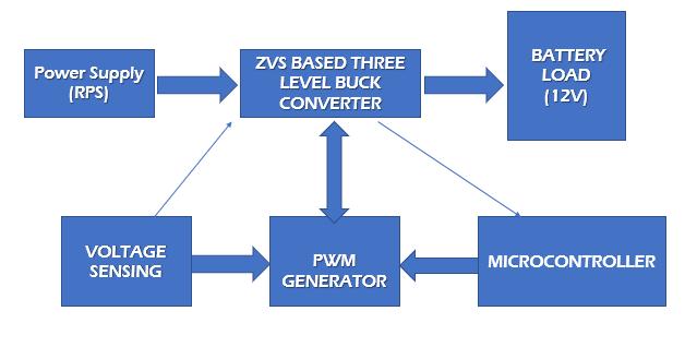
Pulse Width Modulation (PWM) signals generated bya microcontroller or driver IC control the four MOSFETs alternately. Dead-time control ensures ZVS operation, preventingshoot-throughandensuringsoftswitching.The resonantnetworkandpropergatetimingguaranteeminimal switching losses and smooth transitions between voltage levels.
4.BLOCK DIAGRAM

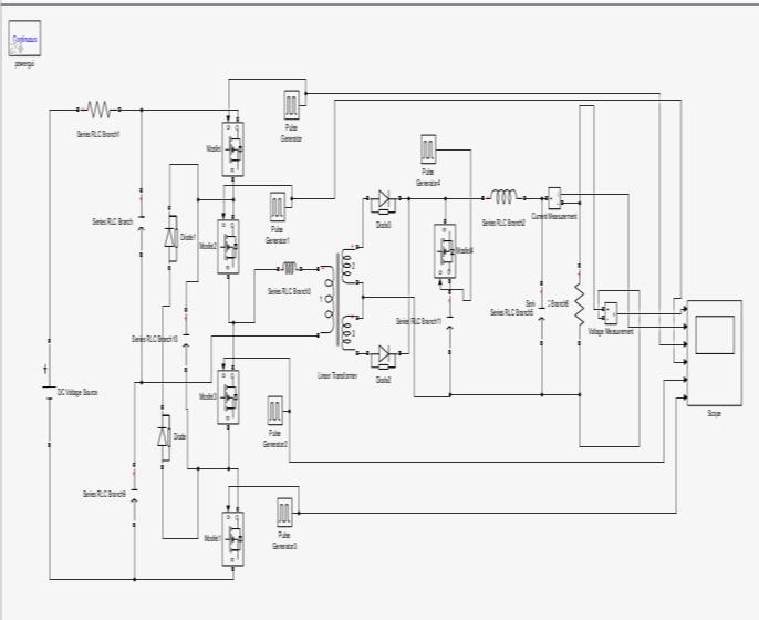
4. CIRCUIT DIAGRAM

Fig.2. SimulinkModelofThreelevelBuckConverterwith ZVSMethod

International Research Journal of Engineering and Technology (IRJET) e-ISSN: 2395-0056
Volume: 12 Issue: 10 | Oct 2025 www.irjet.net p-ISSN: 2395-0072
5.1
Theproposedfour-MOSFET,three-levelbuckconverterwith flyingcapacitorsandaresonantnetworkwasfirstvalidated throughMATLAB/Simulink.Thesimulationmodelincluded:
InputDCvoltage:24V
MOSFETs:Four(S₁–S₄)
Flying capacitors: C₁, C₂ for intermediate voltage levels
Resonantelements:LrandCrforsoft-switching
Outputinductor:L=36µH
Outputcapacitor:C=470µF
Load:Resistiveorbatteryequivalent
Switchingfrequency:50kHz
ThePWMsignalswereappliedthrough gate drivers with properdead-timetoensureZVSoperation.Simulationwas performedunderdifferentloadconditionstovalidateoutput voltage regulation, soft switching, and efficiency improvement.
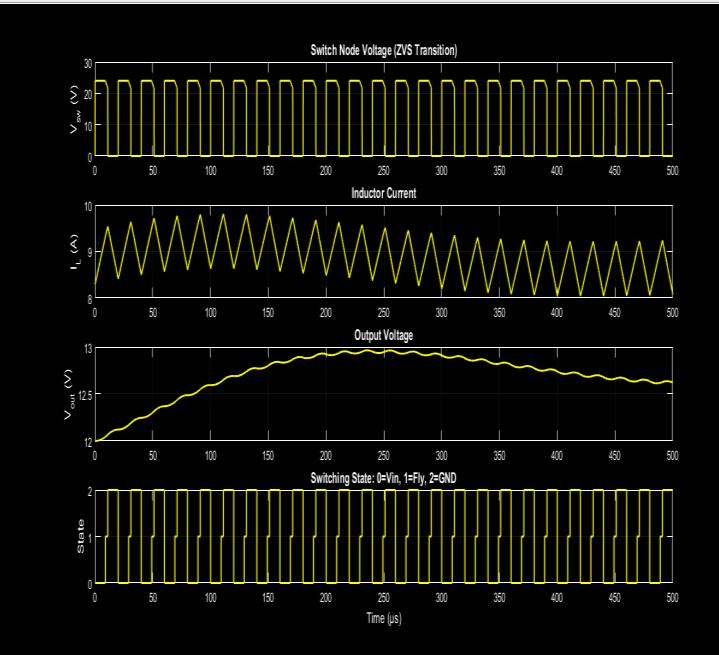
OutputVoltage:Stableintherangeof12–24Vwithminimal ripple.SwitchingWaveforms:MOSFETdrain-sourcevoltage dropped to near zero before turn-on, confirming ZVS. Efficiency: Reduction in switching loss of ~15–20% compared to a conventional buck converter. Thermal Performance:MOSFETtemperaturerisereducedduetosoft switching.
Graphicalresultsinclude:
Outputvoltagevs.time
MOSFETdrain-sourcevoltageandcurrent
Efficiencyvs.load
The hardware prototypeof the proposedthree-level buck converter was developed using four MOSFETs (IRF3205) configured to achieve zero-voltage switching (ZVS) operation.GatedriverICswereemployedtoprovideproper isolation and accurate PWM control. Flying capacitors (C₁ andC₂)wereincorporatedtogenerateintermediatevoltage levels,whilearesonantinductorandcapacitorwereadded to facilitate soft switching. The converter output stage included an output inductor (L) and a resistive load for
stableperformance.A 24V DCsource servedasthe input supply.ThePCBlayoutwascarefullydesignedtominimize parasiticinductanceandresistance,ensuringefficientpower transfer and reduced switching losses. Proper heat sinks were mounted on the MOSFETs to manage thermal performance, and dead-time was introduced in the gate signalstopreventshoot-throughandmaintainreliableZVS operation.
The hardware results of the proposed converter demonstrate effective performance under varying load conditions.Theoutputvoltagewaswell-regulatedwithinthe rangeof12–24V,confirmingstableoperationand proper voltagebalancingthroughtheflyingcapacitors.Oscilloscope observations verified the successful achievement of Zero VoltageSwitching(ZVS),as evidenced bysmoothandsoft transitions in the drain-source voltage waveforms of the MOSFETs.Theconverterattainedamaximumefficiencyof 92–94%atfullload,highlightingtheeffectivenessofthesoftswitchingtechniqueinminimizingswitchinglosses.When comparedwithaconventionalbuckconverter,theproposed designshowedamarkedreductioninswitchinglossesand thermalstress,leadingtoimprovedoverallsystemreliability andenhancedenergyefficiency.
The simulation and hardware results clearly demonstrate theeffectivenessoftheproposedfour-MOSFET,three-level buckconverterwithaflyingcapacitorandresonantnetwork. Simulationanalysisrevealedthattheoutputvoltageripple was significantly minimized due to the proper design of flyingcapacitorsandtheoutputfiltercircuit.Theswitching waveformsconfirmedthatZeroVoltageSwitching(ZVS)was successfullyachievedacrossallfourMOSFETs,asthedrainsourcevoltageapproachedzerobeforeturn-on,resultingin softswitchingoperation.Thisledtoanoverallreductionof approximately15–20%inswitching lossescomparedtoa conventionalbuckconverter,withanoticeabledecreasein MOSFET temperature rise, indicating improved thermal performance. Hardware implementation further validated the simulation findings, where stable output voltage regulationwasobservedforbothresistiveandbatteryloads. OscilloscopewaveformsverifiedtheZVSoperationinallfour switches,andthemeasured efficiencyreached92–94% at fullloadconditions.ThediscussionhighlightsthatthefourMOSFETflyingcapacitortopologyeffectivelyreducesvoltage stress and distributes the switching load among devices, whiletheresonantnetworkensuressoftswitching,thereby minimizingelectromagneticinterference(EMI)andthermal stress.Overall,thecloseagreementbetweensimulationand experimentalresultsconfirmsthepracticalviabilityofthe proposed converter, making it highly suitable for electric vehicle(EV)charging,batterymanagement,andotherhighfrequency,high-powerpowerelectronicsapplication

International Research Journal of Engineering and Technology (IRJET) e-ISSN: 2395-0056
Volume: 12 Issue: 10 | Oct 2025 www.irjet.net p-ISSN: 2395-0072

Futureextensionsofthisworkmayfocusonenhancingthe converter’s performance and adaptability for a broader range of applications. The design can be scaled for higher voltage and current levels to support industrial or commercialelectricvehicle(EV)chargingsystems,enabling operationatgreaterpowerratings.Implementingadigital control strategy using microcontrollers or DSP-based adaptive PWM can further optimize the ZVS operation dynamically under varying load and input conditions, improving overall efficiency. The proposed converter can alsobeintegratedwithrenewableenergysystemssuchas solar or wind applications to enhance energy conversion efficiency and reduce total system losses. In addition, exploring advanced multi-level or hybrid topologies incorporating additional MOSFETs and flying capacitors could further reduce voltage stress and enhance performance. Finally, improving thermal management through active cooling methods, advanced heat sinks, or phase-change materials can ensure reliable and efficient operationinhigh-powerenvironments
8.CONCLUSION AND FUTURE WORK
8.1 Conclusion
Inthiswork,afour-MOSFET,three-levelbuckconverterwith flying capacitors and a resonant network was designed, simulated, and implemented to minimize switching losses using the Zero Voltage Switching (ZVS) technique. The inclusionoftheresonantnetworkenabledZVSoperationin all four MOSFETs, effectively reducing switching losses, lowering thermal stress, and improving overall system reliability.Thethree-leveltopologywithaflyingcapacitor further helped in limiting the voltage stress across each MOSFET to nearly half of the input voltage, which allows higher voltage operation without compromising device safety. As a result, the proposed converter achieved a maximumefficiencyofabout92–94%,whichissignificantly higherthanthatofaconventionalbuckconverteroperating at around 85%. The output voltage remained stable and well-regulatedundervaryingloadconditions,maintaining minimal ripple and ensuring consistent performance. Experimental results closely matched the simulation outcomes, confirming the validity and effectiveness of the four-MOSFETresonantZVStopologyinpracticalhardware implementation. Overall, the developed converter demonstrateshighefficiency,reducedthermalandswitching stress,lowelectromagneticinterference(EMI),andexcellent suitabilityforhigh-frequency,high-powerapplicationssuch aselectricvehicle(EV)batterychargingsystems.
The proposed research work aligns with several United NationsSustainableDevelopmentGoals(SDGs)thatpromote clean energy utilization, sustainable infrastructure, and climate action. The development of a three-level buck converterusingZeroVoltageSwitching(ZVS)techniquefor EV charging systems directly supports these global objectives by improving energy efficiency and reducing powerlosses.
SDG7: Affordable and Clean Energy
Theprojectcontributestothedevelopmentofenergyefficient power conversion systems that enhance the performance of electric vehicle chargers. By minimizing switching losses and improving efficiency, the converter enablesreliableandsustainableenergyusageine-mobility systems.
SDG9: Industry, Innovation, and Infrastructure
Theinnovativethree-leveltopologyandsoft-switching method promote advancements in power electronics, fostering industrial innovation in smart charging infrastructure for electric vehicles and renewable integration.
SDG11:Sustainable Cities and Communities
Electric vehicles play a crucial role in building sustainableandlow-emissioncities.Theproposedefficient converter aids in the widespread adoption of EVs by improvingchargingperformanceandreliability.
SDG13:ClimateAction
Byenhancingenergyefficiencyandsupportingthetransition toelectricmobility,thisprojectcontributestothereduction

International Research Journal of Engineering and Technology (IRJET) e-ISSN: 2395-0056
Volume: 12 Issue: 10 | Oct 2025 www.irjet.net p-ISSN: 2395-0072
ofgreenhousegasemissionsandmitigatesenvironmental impactsassociatedwithfossilfuelconsumption.
[1] Medeiros, A. M., & Santos, J. A. (2025). Four-level ResonantFlyingCapacitorConverterOperatingunder Resonance Featuring Soft-Switching and Voltage RegulationCapabilities Energies,18(5),
[2] Aron, A. (2024). Condensed Buck-Boost Switched Capacitor Converter for High-Efficiency Power Conversion MITEECSThesis Hardwareresultsclosely matchedsimulations,minordeviationsduetoparasitics.
[3] Behrouzi, Y. G., & Behrouzi, Y. G. (2025). High ControllabilitySoftSwitchingStep-UpDC-DCConverter Featuring Coupled Inductor and Voltage Multiplier Techniques Scientific Reports, 15(1), 1777.doi:10.1126/science.1065467.
[4] Li,F.,&Xue,Y.(2025).Soft-SwitchingFixed-Frequency ControlStrategyforThree-LevelBuck-BoostConverter. In 2025 IEEE Workshop on Wide Bandgap Power DevicesandApplicationsinAsia(WiPDAAsia)R.Nicole, “Titleofpaperwithonlyfirstwordcapitalized,”J.Name Stand.Abbrev.,inpress.
[5] Medeiros, A. M., & Santos, J. A. (2025). Four-level Resonant Flying Capacitor Converter Operating with Soft-Switching Energies,18(5),1609