International Research Journal of Engineering and Technology (IRJET)
e-ISSN: 2395-0056
Volume: 04 Issue: 07 | July -2017
p-ISSN: 2395-0072
www.irjet.net
Design and Implementation of Low Power 16-bit Carry-lookahead Adder Using Adiabatic Logic Ashwini A. Pote1, Prof. Ashwini Desai2 IV Semester M.Tech. Student, Dept. of Electronics and Communication Engineering. 2 Faculty Dept. of Electronics and Communication Engineering. 1,2 K.L.E. Dr. M.S.Sheshgiri College of Engineering and Technology, Belagum-590008 Karnataka, India-590018 ---------------------------------------------------------------------***--------------------------------------------------------------------1
Abstract: This paper proposes a two-phase clocked adiabatic static CMOS logic (2PASCL) method for 16bit carry-lookahead adder. The 2PASCAL circuits working on the principles of adiabatic switching can be used for energy recovery. Adders are important components in applications such as digital signal processor (DSP) architectures and microprocessors. Apart from the basic addition, adders are also used in performing useful operations such as subtraction, multiplication, division, address calculation, etc. A schematic and layout of proposed circuit is implemented in Cadence Virtuoso 6.1.5 using 180nm technology. Further power dissipation comparison is made between 2PASCAL and standard CMOS, it shows a significant power saving.
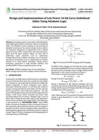
Fig -1: Conventional CMOS charging and discharging. In CMOS circuits charges are fed from the power supply, steered through MOSFET devices, and then dumped into the ground terminal. To change a node's voltage with associated capacitance CL, the circuit is as shown in Figure 2. The energy is extracted from the Vdd terminal. ……… (1) Energy is stored in capacitance …….. (2)
Key Words: 2PASCL adiabatic logic, Carry-Look Ahead Adder, Energy recovery, Power supply, Cadence Virtuoso. 1. INTRODUCTION A demand for portable devices with low power consumption is requirement of today’s electronics world. It is not possible for a customer to carry big batteries with them or charge the battery frequently. If device dissipates more power, internally it heats the system. To cool down the system it requires cooling mechanism, heat sinks and fans. But the device will become more bulky and expensive. For this reason VLSI designers have come up with new approaches to design a VLSI circuit, which consumes less power with increased battery life of a device. Adiabatic logic is one of them, where energy stored at the output node capacitance can be recovered back to the voltage supply. This technique is also referred to as “REVERSIBLE LOGIC”. Static CMOS suffers from power dissipation when a transition occurs in the inputs and a direct path is formed from power supply to ground. Even there is power dissipation when capacitance is discharged through ground, and therefore there is waste of energy. Figure1 shows a charging and discharging path of load capacitance in CMOS logic.
Energy is dissipated in the channel resistance and wire resistance, the amount of dissipated energy depends on the voltage and the amount of charge which flows through, and is independent of the resistance. ………… (3) Later, when this node is connected to the ground, the stored energy is again dissipated. In a cycle, charge is converted into heat [1].
Fig -2: Schematic of a static CMOS inverter.
© 2017, IRJET
|
Impact Factor value: 5.181
|
ISO 9001:2008 Certified Journal
| Page 2914