International Research Journal of Engineering and Technology (IRJET)
e-ISSN: 2395-0056
Volume: 04 Issue: 07 | July -2017
p-ISSN: 2395-0072
www.irjet.net
Implementation of FPGA based Memory Controller for DDR2 SDRAM Sonali R Majukar1, Arun S Tigadi2, Hansraj Guhilot3 PG Student, Electronics and Communication, K.L.E DR. M.S.Sheshgiri Collage of Engineering and Technology, Belagavi, Karnataka, India 2 Assistant Professor, Electronics and Communication, K.L.E DR. M.S.Sheshgiri Collage of Engineering and Technology, Belagavi, Karnataka, India 3 Principal, K. C. College of engineering and management studies and research, Thane, Maharashtra, India ---------------------------------------------------------------------***--------------------------------------------------------------------1
Abstract - Multimedia applications plays very important
role in the field of VLSI design and embedded systems. They need large amount of memory storage with higher bandwidth and higher speed. To overcome this hazard a memory controller is required. A memory controller is a device that stores the data and gives it back whenever required. Real time recording of an audio data and finally storing it without losing the data is difficult task. This paper describes Double Data Rate Synchronous Dynamic Random Access memory controller for storing the audio data. The design uses finite state machine (FSM) architecture that is developed for testing of this algorithm. The tool used to simulate this design is Xilinx ISE design suit. The hardware used to synthesize this design is FPGA Spartan-3 kit.
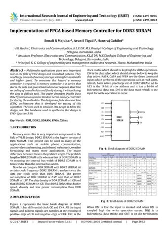
clock enable which should be kept high for all the operations. CS# is the chip select which should always be low to keep the chip active. RAS#, CAS# and WE# are the three command inputs which performs all the operations such as read, write, refresh, bank active, precharge etc of DDR2 SDRAM. A0 to A13 is the 14-bit of row address and it has a 16-bit of bidirectional data bus. DM is the data mask which is the input for write operation to occur.
Key Words: FSM, DDR2, SDRAM, FPGA, Xilinx
1. INTRODUCTION Memory controller is very important component in the field of VLSI design. DDR2 SDRAM is the higher version of DDR SDRAM. This project can be used in many of the applications such as mobile phone communication, audio/video conferencing, audio based web search, weather forecasting and many more applications. The major difference between these is the prefetch length. The prefetch length of DDR SDRAM is 2n whereas that of DDR2 SDRAM is 4n meaning the internal bus width of DDR2 SDRAM is 4 times wider than the external bus width. Now let us compare DDR SDRAM with DDR2 SDRAM. At certain clock frequency DDR2 SDRAM transfers twice the data per clock cycle than DDR SDRAM. The power consumption of DDR SDRAM is 2.5V and that of DDR2 SDRAM is 1.5V. The chip density of DDR SDRAM is 1 GB and that of DDR2 SDRAM is 4 GB. Thus DDR2 SDRAM has higher speed, density and low power consumption then DDR SDRAM.
Fig -1: Block diagram of DDR2 SDRAM
2.IMPLEMENTATION Figure 1 represents the basic block diagram of DDR2 SDRAM. It has differential clock CK and CK#. All the input signals and address signals are samples at the crossing of positive edge of CK and negative edge of CK#. CKE is the Š 2017, IRJET
|
Impact Factor value: 5.181
|
Fig -2: Truth table of DDR2 SDRAM When DM is low the input is masked and when DM is sampled high the write operation occurs. DQS is a bidirectional data strobe and ODT is on die termination ISO 9001:2008 Certified Journal
|
Page 2693