International Research Journal of Engineering and Technology (IRJET)
e-ISSN: 2395 -0056
Volume: 04 Issue: 05 | May -2017
p-ISSN: 2395-0072
www.irjet.net
Power Optimized Voltage Level Shifter Design for High Speed Dual Supply Application Seethal T S1, Mohamed Salih k k2, 1Mtech
scholar, Department of ECE, GECI, Kerala, India Professor, Department of ECE, GECI, Kerala, India ---------------------------------------------------------------------***--------------------------------------------------------------------2Assistant
Abstract – Reduction of power consumption has always
been major design goal in energy harvesting digital devices. One effective way for low power design use of multiple voltages depends on their speed. This, however, accomplish the use of interface block called level converters or level shifters. This paper presents a modified structure of level shifter for lower power implementation. Simulation results of proposed structure in a 0.18-um CMOS technology show that the design of input low supply voltage of 0.4V and high supply voltage of 1.8V, the level shifter has a propagation delay of 12.5ns and a power dissipation of 87.7nW for a 1-MHz input signal. Then comparison is done against these level shifters in terms of power, speed and power delay product. Key Words: CMOS, level converter, subthreshold operation, Dual supply circuits, power delay product.
1. INTRODUCTION Power efficiency and speed are major factor of performance in all digital circuits. Various techniques have used to reduce dynamic and static power. On the other hand, reducing the supply voltage increases the propagation delay of the circuits [2]. In order to avoid these problems dual supply architecture are introduced in which a low voltage (VddL) is supplied for the blocks on the noncritical paths while a high supply voltage (VddH) is applied to the analog and the highspeed digital blocks. Some of the most commonly used techniques are dynamic voltage scaling operating down to near threshold voltage levels and supporting multiple voltage domains .That is why Level shifting circuit is needed to provide exact voltage level for the circuit. A voltage level shifter is one of the major components in a digital system. Level shifters are used for provide correct voltage level for each component in the digital circuits. A wide variety of level shifters have been proposed in the literature review. Designers move their attention to implement a voltage level shifter, which operates minimum power consumption and maximum speed. Moreover the level shifter must able to operate correctly for subthreshold input signals. Some of the recently reported high performance voltage level shifters are reviewed. The proposed circuit introduced in section 3. Section 4 presents the simulation result of the modified circuit verifying the efficiency of the proposed circuit. Finally, concluded in section 5. Š 2017, IRJET
|
Impact Factor value: 5.181
|
Circuit designers are faced with the challenge of developing systems with increasing functionality and complexity while under demanding power and time-to-market constraints. Such systems often require voltage level translation devices to allow interfacing between integrated circuit devices built from different process technologies. The choice of the proper voltage level translation device depends on many factors and will affect the performance and efficiency of the circuit application. Thus voltage level shifters play an important role in widely used VLSI systems. Voltage level translation is needed when two devices have differing supply voltage nodes. Two possible conditions exist. A higher-voltage device may be needed to drive a lowvoltage device. A lower-voltage device may be needed to drive a high-voltage device. If the low voltage device is the driver, the circuit typically cannot function properly without the use of a translation device.
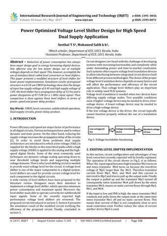
Fig-1: Voltage levelshifter functioning
2. EXISTING LEVEL SHIFTER IMPLEMENTATION In this section, circuit configuration and advantages of two level converters recently reported will be briefly explained. The operation of the circuit shown in Fig.2, is as follows. When the input signal becomes high transistor Mn1 turns on and nmos transistor Mn4 turns on because the overdrive voltage of Mp3 larger than the Mn3. Therefore transition current flows Mp1, Mn1, and Mn4 and this current is mirrored to Mp2 and tries to pull up the output node. Finally the output is pulled up and the transistor Mp3 turned off consequently nmos transistor Mn4 pull down by the nmos transistor Mn3, means no static current flows through Mp1, Mn1, and Mn4. If the input is low and INB is high, the nmos transistor Mn2 conducts and pulls down the output node at the same time nmos transistor Mn1 off and no static current flows. This means that current of Mp2 is not completely close to zero weak contention exist. Further reduce the value of current another device Mp4 is used.
ISO 9001:2008 Certified Journal
|
Page 548