International Research Journal of Engineering and Technology (IRJET)
e-ISSN: 2395 -0056
Volume: 04 Issue: 04 | Apr -2017
p-ISSN: 2395-0072
www.irjet.net
Review on Modified Gate Diffusion Input Technique Divya Soni1, Mihir V. Shah2 1 PG
Student, Department of E & C, LD College of Engineering, Ahmedabad, India Department of E & C, LD College of Engineering, Ahmedabad, India ---------------------------------------------------------------------***--------------------------------------------------------------------2Professor,
Abstract - This paper gives an overview upon MGDI
The current paper is organized into 5 sections. Section 1 gives introduction. Section 2 gives description of GDI technique. Section 3 gives description of MGDI technique. Section 4 gives brief literature survey. Finally, the paper is concluded with section 5.
technique, in which low number of transistors are used that reduce the power consumptions and area on chip of digital circuits. In this paper full adder is introduced using MGDI technique. 2 bit comparator, full subtractor were introduced using GDI technique. Then these digital circuits were compared with traditional CMOS transistors in terms of power dissipation, number of transistors, area, speed and delay.
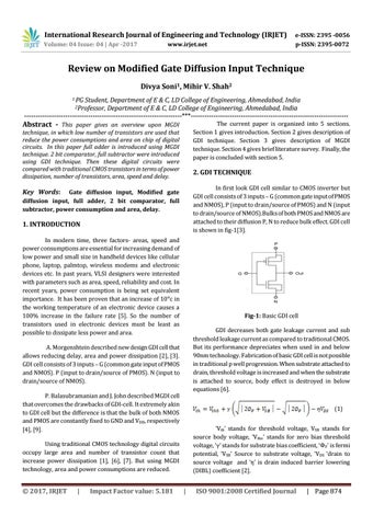
2. GDI TECHNIQUE In first look GDI cell similar to CMOS inverter but GDI cell consists of 3 inputs – G (common gate input of PMOS and NMOS), P (input to drain/source of PMOS) and N (input to drain/source of NMOS).Bulks of both PMOS and NMOS are attached to their diffusion P, N to reduce bulk effect. GDI cell is shown in fig-1[3].
Key Words:
Gate diffusion input, Modified gate diffusion input, full adder, 2 bit comparator, full subtractor, power consumption and area, delay.
1. INTRODUCTION In modern time, three factors- areas, speed and power consumptions are essential for increasing demand of low power and small size in handheld devices like cellular phone, laptop, palmtop, wireless modems and electronic devices etc. In past years, VLSI designers were interested with parameters such as area, speed, reliability and cost. In recent years, power consumption is being set equivalent importance. It has been proven that an increase of 10ᵒc in the working temperature of an electronic device causes a 100% increase in the failure rate [5]. So the number of transistors used in electronic devices must be least as possible to dissipate less power and area.
Fig-1: Basic GDI cell GDI decreases both gate leakage current and sub threshold leakage current as compared to traditional CMOS. But its performance depreciates when used in and below 90nm technology. Fabrication of basic GDI cell is not possible in traditional p well progression. When substrate attached to drain, threshold voltage is increased and when the substrate is attached to source, body effect is destroyed in below equations [6].
A. Morgenshtein described new design GDI cell that allows reducing delay, area and power dissipation [2], [3]. GDI cell consists of 3 inputs – G (common gate input of PMOS and NMOS). P (input to drain/source of PMOS). N (input to drain/source of NMOS). P. Balasubramanian and J. John described MGDI cell that overcomes the drawbacks of GDI-cell. It extremely akin to GDI cell but the difference is that the bulk of both NMOS and PMOS are constantly fixed to GND and VDD, respectively [4], [9].
(1) ‘Vth’ stands for threshold voltage, VSB stands for source body voltage, ‘Vtho’ stands for zero bias threshold voltage, ‘γ’ stands for substrate bias coefficient, ‘ФF’ is fermi potential, ‘VSB’ Source to substrate voltage, ‘VDS ‘drain to source voltage and ‘η’ is drain induced barrier lowering (DIBL) coefficient [2].
Using traditional CMOS technology digital circuits occupy large area and number of transistor count that increase power dissipation [1], [6], [7]. But using MGDI technology, area and power consumptions are reduced.
© 2017, IRJET
|
Impact Factor value: 5.181
|
ISO 9001:2008 Certified Journal
| Page 874