International Research Journal of Engineering and Technology (IRJET) Volume: 04 Issue: 02 | Feb -2017
e-ISSN: 2395 -0056
www.irjet.net
p-ISSN: 2395-0072
Design and Implementation of Phase Frequency Detector Using Different Logic Gates in 45nm CMOS Process Technology Hiren B. Ravisaheb 1, Bharat H. Nagpara 2 1P.G.
Student, Dept. of EC, C. U. Shah College of Engineering & Technology, Wadhwancity ,Gujarat Prof. , Dept. of EC, C. U. Shah College of Engineering & Technology, Wadhwancity, Gujarat.
2Asst.
---------------------------------------------------------------------***---------------------------------------------------------------------
Abstract - The Phase Detectors determines the relative
characteristics
phase difference between the two incoming signals and outputs a signal that is proportional to this phase difference. The phase detector also detects the frequency error; they are called Phase Frequency Detectors (PFD). It is very important block for the Clock and Data Recovery circuit. This paper presents the different design schemes of the PFD and compares them with their output results. The PFD is implemented with True Single Phase Clocked logic. The circuits that have been considered are the PFD using NAND Gate, PFD using NOR Gate and PFD using AND Gate. The different PFD circuits are designed and simulated on LT Spice Tool using 45nm CMOS process technology with supply voltage 1 V.
frequency
detector.
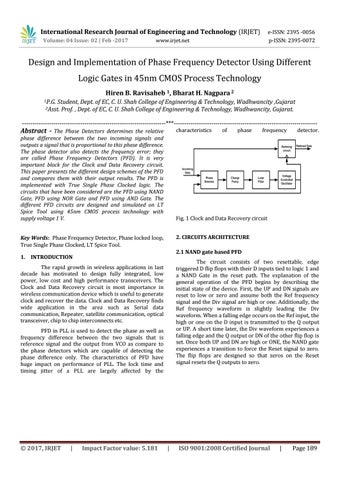
2. CIRCUITS ARCHITECTURE 2.1 NAND gate based PFD
1. INTRODUCTION
The circuit consists of two resettable, edge triggered D flip flops with their D inputs tied to logic 1 and a NAND Gate in the reset path. The explanation of the general operation of the PFD begins by describing the initial state of the device. First, the UP and DN signals are reset to low or zero and assume both the Ref frequency signal and the Div signal are high or one. Additionally, the Ref frequency waveform is slightly leading the Div waveform. When a falling edge occurs on the Ref input, the high or one on the D input is transmitted to the Q output or UP. A short time later, the Div waveform experiences a falling edge and the Q output or DN of the other flip flop is set. Once both UP and DN are high or ONE, the NAND gate experiences a transition to force the Reset signal to zero. The flip flops are designed so that zeros on the Reset signal resets the Q outputs to zero.
The rapid growth in wireless applications in last decade has motivated to design fully integrated, low power, low cost and high performance transceivers. The Clock and Data Recovery circuit is most importance in wireless communication device which is useful to generate clock and recover the data. Clock and Data Recovery finds wide application in the area such as Serial data communication, Repeater, satellite communication, optical transceiver, chip to chip interconnects etc. PFD in PLL is used to detect the phase as well as frequency difference between the two signals that is reference signal and the output from VCO as compare to the phase detectors which are capable of detecting the phase difference only. The characteristics of PFD have huge impact on performance of PLL. The lock time and timing jitter of a PLL are largely affected by the
|
phase
Fig. 1 Clock and Data Recovery circuit
Key Words: Phase Frequency Detector, Phase locked loop, True Single Phase Clocked, LT Spice Tool.
Š 2017, IRJET
of
Impact Factor value: 5.181
|
ISO 9001:2008 Certified Journal
|
Page 189