
International Research Journal of Engineering and Technology (IRJET) e-ISSN: 2395-0056
Volume: 12 Issue: 08 | Aug 2025 www.irjet.net p-ISSN: 2395-0072

International Research Journal of Engineering and Technology (IRJET) e-ISSN: 2395-0056
Volume: 12 Issue: 08 | Aug 2025 www.irjet.net p-ISSN: 2395-0072
Rakshitha S Nayaka1 , A.N. Nagashree2 , Gautham Vishal3, Suriya S4, Santosh B L5 , Bhoopendra Kumar Singh6
1PG Student, BMS College of Engineering, Bengaluru
2Proffesor, Dept of EEE, BMS College of Engineering, Bengaluru
3Senior Engineer, Centum Electronics Ltd, Bengaluru
4Senior Engineer, Centum Electronics Ltd, Bengaluru
5Assistant Manager, Centum Electronics Ltd, Bengaluru
6Director, Centum Electronics Ltd, Bengaluru
Abstract- Power supply modules have become an important part of modern power electronics. They provide stable power delivery for a wide variety of applications. DC-DC power converters are used for various applications and particularly very useful for space application toprovidearegulatedoutputpower. Amongvariousdc-dc converter topologiesthefly-back and forward converters provide isolation and hence more frequently used for space applications, wherein isolation isnecessary.The present paperdescribesthe design and implementation of an 80W dual output forward converter with input voltage feed-forward controltechnique,foraswitchingfrequencyof140kHz. UC2525 PWM controller has been implemented due to itsfastresponse,soft startcapabilities,Under-Voltage protection and maximum duty cycle control. The converter is designed with an isolation transformer and a mag-amp for secondary output voltage control. The analysis and hardware implementation of the prototype converter is developed and tested for different input voltages and load conditions at ambient temperature to validate the results.
Key Words:DC-DCConverter,InputVoltageFeed-Forward Control,Mag-Amp,PowerSupplyModule,PWMController, SwitchingFrequency.
Apowersupplymoduleisadeviceconnectedintermediate topowersourceandelectronicload.Itsprimaryfunctionisto converttheelectricalenergyinthepowersupplytoasuitable formforusebytheload.DC-DCconvertersareusedinawide varietyofapplications,
suchaspowersuppliesforcomputers,consumerelectronic devices,UPS,telecommunicationsequipmentetc.Aregulated DCpowersupplyiscriticalforoptimalandefficientoperation of an electronic system. While most power supplies are designed to deliver the necessary features like regulated
power output, electrical isolation, and multi-output capability, there are some common objectives for power supply design such as: minimal size, minimal weight and increasedefficiency[1].
TheDC-DCconvertertopologyconsistsofBuck,Boost,BuckBoost, Cuk, Sepic, Fly-back, Forward, Half Bridge and Full Bridge Converters. Among these converters, forward converter topology is selected for designing power supply module [1]. It has many advantages over various other topologies such as, good reliability, compact size, more efficientandisoftenchosenforoutputpowerunder200W. Forproperloadregulation,amagneticamplifier(mag-amp) hasbeenimplementedinthesecondarysideoftheconverter. AmagneticamplifierorMag-Ampisanelectronicamplifier thatusesmagneticpropertiestocontroltheflowofelectrical current. The Mag-Amp provides robustness and radiation tolerancewhichmakesitwellsuitableforspacebornepower supply [2]. Implementing a magnetic amplifier (mag-amp) providesseveralnotableadvantagessuchas:
i) Largecurrentscanbehandledbysmallcore.Also,thereis noneedforheatsink.Thisresultsinsmallermountarea,thus achievingminiaturization.
ii)The power needed for control of mag-amp is smaller, enabling power to besaved.
iii)Asthemagneticamplifierisconnectedinserieswitha diode,thenoisefromtheoutputofthediodeisless.
iv) Since mag-amps are magnetic parts, the cores are not destroyedbysurgesin voltageandcurrent.
v)Themag-amprealizespreciseoutputvoltagebecausethe transformer’ssecondaryisdirectlycontrolled[2].

Volume: 12 Issue: 08 | Aug 2025 www.irjet.net p-ISSN: 2395-0072
2.1
The converter chosen for this application is a forward converterwithtwoMOSFETsconnectedinparallelanddual output. It utilizes a transformer to provide electrical isolationandeithertostepuporstepdownthevoltage.In low power applications (typically under 50 W), single MOSFET is acceptable. However, in medium power applications(50to200W),twoMOSFETsareconnectedin parallel to share the current hence resulting in decreased thermal losses without using a full-bridge or half-bridge carriercurrent.
2.2 Working Principle
TheproposedforwardconvertercircuitisshowninFig1.It consistsofafast-switchingMOSFETdevice,a transformer with its primary winding in series with the switch to the unregulatedinputsupplyandadioderectifierfollowedbya filterwhichisconnectedtothesecondaryside.Theloadis connected across the rectified and filtered end of the secondary[3].
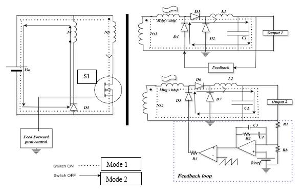
Theconverteroperatesintwodistinctmodesbasedonthe switchingstates:
(a) Mode 1 –When the switch is turned ON
(b) Mode 2 –WhentheswitchisturnedOFF
Mode 1 Operation:
This mode is called the power transfer function mode as showninFig1.Thecurrentflowsfromtheinputsourceto theloadthroughthetransformerandfilternetwork.
Inthismode,themainswitch(S1)isinONstate.Indicating thattheinputvoltageisappliedacross the primaryof the transformer. Current flows through the primary of the transformer as shown in Fig 1. With respect to the transformer dot convention, a corresponding voltage is inducedonthesecondarysidewhichallowsenergytransfer fromtheprimarytothesecondary.
Whileswitch(S1)is'ON',theforwardpathdiodesD1and D6becomeforward-biasedandallowthesecondarycurrent flows through the low-pass filter, which consists of an inductor(L)andacapacitor(C).Thislow-passfilterallows the majority of high frequency ripple components to be attenuated,allowingtheloadtobesuppliedwithasteadyDC output.Meanwhile,thefreewheelingdiodesD4andD5stay OFFbecausetheyarereverse-biased.Similarly,thediodeD3 on the primary side, remains off due to the opposite dot position, basicallyimplying reverse biased condition.This modeiscalledthepowertransferfunctionmode,because the energy is flowing from the input source to the load throughthetransformerandfilternetwork.
ThismodeiscalledthefreewheelingmodeasshowninFig1. Itcommenceswhenthemainswitch(S1)isturnedOFFand thecurrentinthetransformerprimarywindinggoestozero. Thus,theoutputfilterinductoronthesecondarysidebuilds up the current to the load and returns through the freewheeling diodes D4 and D5. While this occurs, the forwardpathdiodesD1andD6arereverse-biased.Onthe primary side, when the dot polarity reverses between the primaryandresetwindings,diodeD3isforwardbiasedand startstoconduct,thusallowingthemagnetizingcurrentto circulateinthereversedirectionandbeginthecorereset.
Toimprovetheregulationandeliminateoperationundera minimumloadconditioninaforwardconverter,amagnetic amplifier(mag-amp)isconnectedateachoutput.Withthis scheme, the master output provides feedback control for changeindutycycle,whileamag-ampcontrolsregulation independentlyforeachoutput.Theoverallmag-ampcontrol circuitisshowninFig2(a)andmag-ampof6-L2016-W763 (NanocrystallineCore)isshowninFig2(b).

International Research Journal of Engineering and Technology (IRJET) e-ISSN: 2395-0056
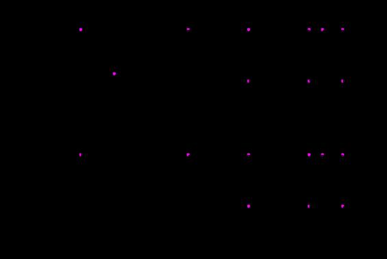
Fig2(a):Mag-Ampcontrolcircuit.
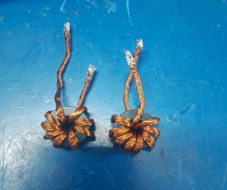
Fig2(b):6-L2016-W763(NanocrystallineCore).
Thisarchitecture removes theneedforfeedback fromthe output to the input side, resulting in a faster dynamic response. Furthermore, it allows each output to regulate independently from no-load condition, eliminating the minimumloadconstraint.
Voltage Feed-Forward
Theinputvoltagevariationmayautomaticallychangethe duty cycle hence degrading the performance of the converter.Thisrequiresaclosedlooptocorrecttheoutput dutycycle.Infeed-forwardtechnique,thePWMdutyratio changeswithchangeininputvoltageandhencemaintaining constantoutputvoltage.AnRCnetworkgeneratesarampor sawtoothwaveformwhichisdependentontheinputvoltage as shown in Fig 3(a) [4]. The generation of the ramp is dependent on the input voltage, for example if the input voltage doubles, the ramp waveform slope also increases proportionally and the duty cycle will tend to decrease as showninFig3(b)[4].
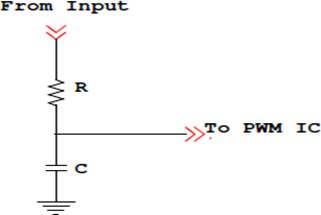
Fig3(a):RCnetwork[4]
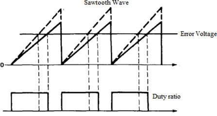
Fig3(b):Variationofdutycyclewithinputvoltage[4]
Thistechnique(Voltagefeedforward)providespreemptive correctionoftheoutputdutycycleasiteliminatesthedelay when compared to a feedback control loop. In feedback controlloop,thecorrectionismadefromanerroramplifier only after it responds to changes that are detected at the output.Henceinvoltagefeed-forwardmethod,theresponse timeandvoltagecontrolaremuch fasterandwithgreater accuracy.
Ina dual-outputforwardconverter,twoMOSFETscan be wiredinparallelontheprimarysideasshowninFig4.
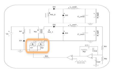
Fig4:ForwardConverterwithtwoMOSFETsinParallel
Thiswillsupporthighcurrentandimprovedefficiency.The aimforparallelingistosharethecurrentbetweenthetwo devicesthusloweringthestressoneachindividualswitch,
Volume: 12 Issue: 08 | Aug 2025 www.irjet.net p-ISSN: 2395-0072 © 2025, IRJET | Impact Factor value: 8.315 | ISO 9001:2008 Certified Journal | Page83

International Research Journal of Engineering and Technology (IRJET) e-ISSN: 2395-0056
Volume: 12 Issue: 08 | Aug 2025 www.irjet.net p-ISSN: 2395-0072
soastominimizetheconductionloss.Sincethepowerlosses are shared between the two devices, the total loss is split between the two devices which results in lower heat dissipation. Hence the efficiency of the converter also increases.Thus,parallelingoftwoMOSFETsensuresbetter performancefortheoverallsystem.Thetwoparalleldevices havereducedthermallimitations,moresymmetricalthermal distributionandrunsmorereliablywhenoperatingunder maximumload.
3.1 Methodology
Thebriefstructureofmethodologyfortheproposedworkis showninFig5.

Fig5:Methodology
Planning:
•Asuitableconvertertopologywasselectedbasedonthe givenspecifications.
• The topology selected for this application is Forward Converter.
Block Diagram and Schematic Design:
• Both block diagram and circuit schematic were created fromthestatedrequirements.
•SoftwareutilizedwasLTSpice,OrCAD,andMathcad.
•ABOMwascreatedafterthecompletionoftheschematic.
Selection of Components:
•Componentswereselectedbasedonthepreviousdesign calculations.
• Considerations when selecting components includes: powerratings,tolerancesandthermalability.
Design Analysis and Hardware Implementation:
•AfterthedesignandBOMwerefinished,multipleanalyses were conducted such as, Derating analysis, Power dissipationcalculationandFeasibilityanalysis.
•Aftertheanalysisphase,hardwarewasbuiltbasedonthe schematic.
Testing and Verification:
•Thebuiltconverterunderwentmultipletestsincluding, ImpedancetestsandThermaltests.
•Finally,thedesignperformancewascomparedagainst expectedoutcomes.
Theblockdiagramofproposedforwardconverterisshown inFig6.
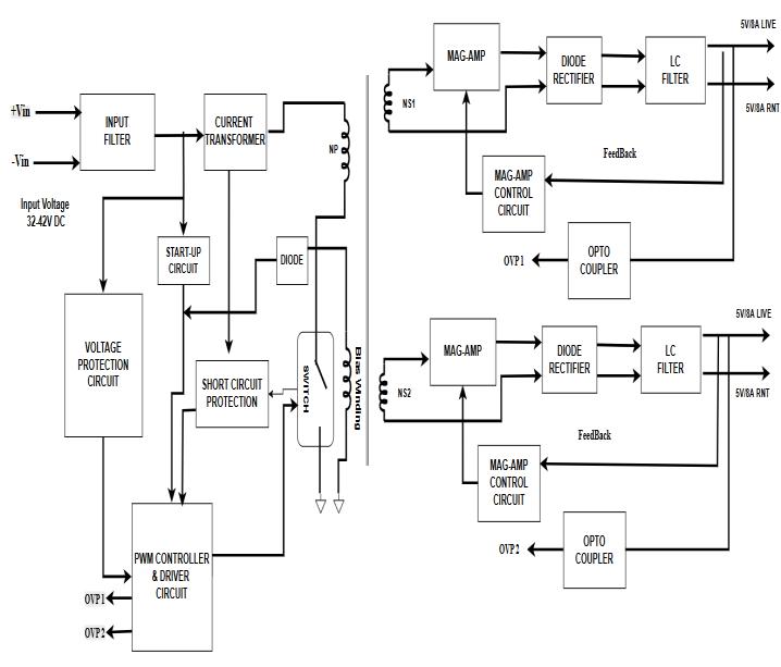
The developed power module is designed to deliver dual outputsof5V/8Aeach,providingacombinedoutputpower of 80W. The input to the DC-DC converter is a variable voltageof32V-42VDCandgivestworegulatedoutputsat 5V/8Aeach
Theblockdiagramofproposedforwardconverterhasthe followingblocks:
i) Input Protection and Filtering ii) Startup Circuit iii) Voltage Protection Circuit iv) PWM Controller and Gate Driverv)MagneticAmplifier(MagAmp)vi)Optocoupler.
i) Input Protection and Filtering:
In order to protect the converter from instances of overvoltageandovercurrent,relaysareutilizedontheinput side.Therelaysprovidealevelofsafetyfortheoperationof the entire power system. An EMI (Electromagnetic Interference) filter is also placed on the input stage to eliminatetheunwanted effectsofcurrent,harmonics,and electrical noise. The EMI filter enhances the converter’s efficiencyandreliabilitybysupplyingnoise-freeDCpowerto thetransformer'sprimary.
ii)Startup Circuit:
Itconvertsthereferencecircuitryfromazero-currentstate tonormalcondition.Oncethereferencecircuitisenergized and stable, the startup circuit is no longer required or needed,andbecomesinactive.

International Research Journal of Engineering and Technology (IRJET) e-ISSN: 2395-0056
Volume: 12 Issue: 08 | Aug 2025 www.irjet.net p-ISSN: 2395-0072
iii)Voltage Protection Circuit:
Thecircuitincludesanovervoltageprotectioncircuit(OVP) whichallowstheoutputtobehaltedbeforethevoltagecan exceed a level of safety. In this design, the OVP threshold occursat44V, while the undervoltage protection (UVP) is trippedwhentheinputvoltagefallsbelowavalueof30V.
iv)PWM Controller and Gate Driver:
ThePWMcontrollerisamodifiedversionwhichisusedin varioushighfrequencyswitchedmodepowersupply(SMPS) applications to control output voltage based on change in input voltage. Additionally, a gate driver circuit is implemented that drives the power switches while maintainingelectricalisolationfromthepowerstage.Gate driver circuits provide high noise immunity and good reliability when transferring a signal to the gates of the powerswitches.
v)Magnetic Amplifier (Mag Amp):
Amagneticamplifier(Mag-Amp)hasbeenimplementedon the transformer secondary side to regulate the output voltage.Theoperationofamagneticamplifierreliesonthe principlesofcoresaturationwithtransformer.Inamagnetic amplifier, the magnetic properties are used to control the flowofelectricalcurrent.
vi)Optocoupler:
Attheoutputside,anoptocouplerisincludedtocontroland communicatevarioussignalsbetweenisolationareasinthe circuit.TheoptocouplerconsistsofaninternalinfraredLED andaphotosensitivedetectortoprovidegalvanicisolation. The isolated part of the circuit provides signal communications without electrical connection between circuits.
4. SPECIFICATION AND DESIGN OF PROPOSED CONVERTER SYSTEM
Thedesignspecificationsoftheproposedforwardconverter aresummarizedinTable1.
Table1:ProposedForwardConverterSpecification
Parameter
Specification
InputVoltageRange 32V–42VDC
SelectedTopology IsolatedForward Converter
OutputVoltage (foreachoutputs) 5V
OutputCurrent (foreachoutputs) 8A
SwitchingFrequency
This section highlights the design aspects of key components,including:a)Transformerdesign.b)Selection ofswitchingdevice.c)Designofoutputfilter.d)Selectionof secondarydiode.
Thetransformerdesignparameters,Areaoftheconductor andnumberofturnsareshownbelow[5].
Vinmin=32VDC
Vinmax=42VDC
Kw=0.35
Bm=0.12Tesla
J=6Amp/mm2
Fsw=140KHz
Pout=80Watts (1)


International Research Journal of Engineering and Technology (IRJET) e-ISSN: 2395-0056
Volume: 12 Issue: 08 | Aug 2025 www.irjet.net p-ISSN: 2395-0072


Selectedcore: 0R43019UG, material, Ur:5010, AL: 6680mH/1000T.
Where,
Kw=WindowFactor
J=CurrentDensityA/mm2
Fsw=SwitchingFrequencyHz
Dmax=MaximumDutyCycle
Bm=MaximumFluxDensityT
Vd=DiodeDrop
Selection of Mag-Amp Core:
Basedontheareaoftheconductor,themag-ampis selectedasperthefollowingdesign[5].

Where,
Apma=AreaproductofMag-Amp
Ax=Wireareaofconductor
Vwithstand=Withstandingvoltage
Bm=MaximumFluxDensityT
Vd=DiodeDrop
SelectedMag-AmpCore:
P/N:6-L2016-W763(NanocrystallineMag-AmpCore)
4.2.2 Selection of switching device:
Switchingdevicesinpowerconvertersundergoextremely highelectricalstresslevelsbecausethereisrapidchangein voltage and current. Thus, it is very important to select a proper switching device when designing switching converters.Commonlyuseddevicesincludediodes,bipolar junctiontransistors(BJTs),metal-oxide-semiconductorfieldeffect transistors (MOSFETs) and insulated gate bipolar transistors(IGBTs)[5].
MOSFETsarepreferredin:
• Highfrequencyapplications(>200kHz).
• Wide range of line variations or load variations.
• Deviceofchoiceforblockingvoltagesless than500V.
• A majority-carrier device: fast switching speed.
Conduction loss: Conduction losses are the power losses occurringinMOSFETwhileconducting,reliesmainlyonthe RMScurrentflowingintheswitchandONstateresistance dropfromdraintosource.Byselectingthelowerresistance value,theconductionlossescanbeminimized[6].
Switching loss: Switching losses are associated with the transitionofswitchesfromONtoOFFstateandvice-versa. The losses are related to the Gate charge (Qg), switching frequency,andswitchingvoltageneededforGatetoturnON theMOSFETswitch.Therefore,themosfetisselectedinan optimalwaysothatlossesareminimized[6].
Thepeakvoltageofthemosfetiscalculatedbyusing belowequation,

Selected MOSFET: IRHM57260, 200V, 0.049 Ohm, 32@ 100 Deg
4.2.3
Theoutputvoltageoftransformersecondaryisprocessed through rectification and filtering to obtain the required output.Intheproposedconverter,anLCfilterisemployed and selecting appropriate component values is essential. Properfilterdesignhelpstominimizenoise,reducesizeand lower costs, which are key considerations for spaceborne applications.
The design formulae for output inductor and output capacitorarementionedinthebelowequations.


International Research Journal of Engineering and Technology (IRJET) e-ISSN: 2395-0056
Volume: 12 Issue: 08 | Aug 2025 www.irjet.net p-ISSN: 2395-0072
Whenselectingtheoutputdiodeforagivenapplicationitis determined by the voltage and current levels of the secondary side. Schottky diodes are the preferred choice, becausetheyhavealowforwardvoltagedrop(approx.0.6 V)andcanhandlesubstantialcurrent(approx.35A).
One advantage of a Schottky diode over conventional p-n junctiondiodesisthattheyhavenegligiblereverserecovery time(Trr).Whilea p-ndiodewillhaveareverserecovery time of several hundred nano seconds changing from a conductionstateto a blockingstate,Schottkydiodeshave virtuallynotimedelay.
ThismakesSchottkydiodeswell-suitedforhigh-frequency applicationswherelowforwardvoltagedrop,highcurrent handlingandverylowreverserecoverytimearerequired [5].
Selected Diode is 35CGQ150, Package: TO-254AA having VF=150V,IF=35A,VFD=0.6V
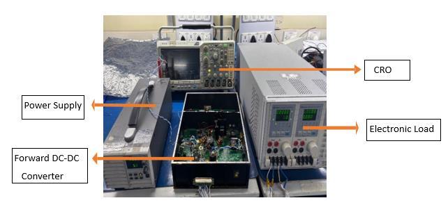
Fig 7 illustrates the hardware experimental setup of the forwardconverter.Thekeycomponentsofthiscircuitsetup includethefollowing:
• Powersupply
• CathodeRayOscilloscope(CRO)
• Forwarddc-dcconverter
• Electronicload
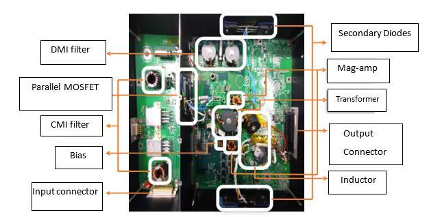
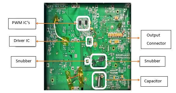
The top view and bottom view of the proposed forward converteraredepictedinFig8andFig9respectively.The primarykeycomponentsusedinthehardwaresetupofthe proposedforwardconverterareasfollows:
EMIfilter(CMI&DMIfilters)
Transformer
Inputandoutputconnectors
ParallelMOSFETs
Biasinductor
SecondarydiodesandMag-Amps
Outputcapacitorsandinductors
Snubbercircuit
PWMIC&DriverIC
The gate and drain waveform for different input voltage condition(32V,36Vand42V)isshowninFig10(a),10(b) and 10(c) whichconsistsofmaximumand peak-peak gate voltageanddrainvoltage.

International Research
Volume: 12 Issue: 08 | Aug 2025 www.irjet.net p-ISSN: 2395-0072
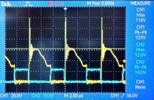
10(a):Gate&Drainwaveformforinputvoltageof32V
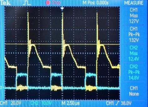
Fig10(b):Gate&Drainwaveformforinputvoltageof36V
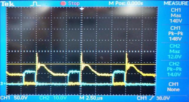
Fig10(c):Gate&Drainwaveformforinputvoltageof42V
Drain Voltage: Thepeakdrainvoltageoccursatmaximum inputvoltageandmaximumload.Theenergyregenerative snubber circuit used and the reduction of transformer leakageinductancemitigatestheringingpresentinthedrain voltage.ThisreductioninvoltageringingacrosstheMOSFET leads to a reduction in switching losses and therefore improvesconverterefficiency.
Table2:Gate&Drainvoltageatdifferentinputvoltages.
6.2 Output Voltage:
TheTable3 andTable 4shows theoutput-Iand output-II voltagesatdifferentinputvoltage(32V,36Vand42V)andfor differentloadconditionsi.e.,10%,50%and100%.
Table3:OutputVoltages-Output-I
Table4:OutputVoltages-Output-II
6.3 Output Ripple Voltage:
RipplevoltagereferstotheACcomponentsuperimposedona DCoutput.Itisakeyparameterinevaluatingthequalityof the DC voltage. Measurements of ripple voltage were conductedundervaryingloadconditionsandinputvoltage levels.ThemeasuredvaluesarepresentedinTable5.
Table5:Ripplevoltagesforoutput-I(5V/8A).
Themeasuredoutputvoltagerippleforoutput-IIisassame asoutput-I(Table5).
6.4 Line and Load Regulation:


International Research Journal of Engineering and Technology (IRJET) e-ISSN: 2395-0056
Volume: 12 Issue: 08 | Aug 2025 www.irjet.net p-ISSN: 2395-0072
Thelineregulationfordifferentinputvoltageisshownin Table6.
Table6:LineRegulation
LoadRegulationisdefinedby,
specifications. The use of magnetic amplifier (mag-amp) provides improved load regulation (<2%) by controlling eachoutput.Additionally,thevoltagefeed-forwardcontrol techniqueensureseffectivelineregulation(<1%)byoffering a fast-dynamic response. The output voltage ripple is maintainedwithintheacceptablelimits,withapeak-to-peak ripple of less than 50 mV, ensuring stable and noise-free powerdelivery.Hencetheproposedconverterisfoundtobe suitableforspacebornepowersupplyapplications.

%LoadRegulation= (14)
Theloadregulationfordifferentinputvoltageisshown inTable7
Table7:LoadRegulation
Condition
6.5 Efficiency:
Efficiencyundervariousoperatingconditionsisdetermined by measuring the input and output power. The calculated efficiencyvaluesareshowninTable8.

Table8:Efficiencyobtainedatvariousloadconditions withdifferentinputvoltageconditions.
7. CONCLUSION
Design and Implementation of 80W Dual Output Forward Converter for Spaceborne Power Supply Applications is carried out. As per the results obtained, the converter efficiency is above 65% thus meeting the design
The authors express their sincere gratitude to the ManagementofBMSEducationalTrust,thePrincipalandVice Principals of BMS College of Engineering and Centum Electronics Ltd. for their continuous support and encouragementthroughoutthiswork.
[1] Madhura G O, A.N Nagashree, Santhosh B L, Bhoopendra Kumar Singh, “Design and ImplementationofSingleOutputHighFrequency Forward Converter using Mag-Amp for Space Application”,ZeichenJournal,Issue:08Volume:10.
[2] S.R.Savanur,S.Patil,B.SinghandV.chippalkatti, "HardwareImplementationofForwardConverter with Active Clamp Reset Technique," 2020 InternationalConferenceonSmartTechnologies in Computing, Electrical and Electronics (ICSTCEE), Bengaluru, India, 2020, pp. 293-297, doi:10.1109/ICSTCEE49637.2020.9276794.
[3] Suman V, A.N Nagashree,, Bhoopendra Kumar Singh, “Design and Implementation of Multiple Output Forward Converter with Input Voltage Feed Forward Control for Space Applications”, Zeichenjournal–AUGCCareapprovedgroupII journal,Volume7issue8ISSN0932-4747.
[4] Sahana J 1, Dr. Anitha G S, T K Nagaraju, Bhoopendra Kumar Singh, “Design and ImplementationofaRobustDualoutputForward Converter for Space Application”, International ResearchJournalofEngineeringandTechnology” (IRJET)Volume11Issue08,Aug2024.
[5] AshishKumarNHandDr.AnithaGS“Designand ImplementationofEfficientDC-DCConverterwith Forward Converter Topology for Low Power Applications”, International Research Journal of EngineeringandTechnology”(IRJET)Volume11 Issue08,Aug2024.
[6] J.Rodríguez,J.R.García-Mere,D.G.Lamar,M.M. Hernando and J. Sebastián, "High Step-Down

International Research Journal of Engineering and Technology (IRJET) e-ISSN: 2395-0056
Volume: 12 Issue: 08 | Aug 2025 www.irjet.net p-ISSN: 2395-0072
Isolated PWM DC–DC Converter Based on CombiningaForwardConverterWiththeSeriesCapacitorStructure," inIEEEAccess,vol.11,pp. 131045-131063,2023.
[7] K.Hata,S.Suzuki,K.Watanabe,K.Nagayoshi,and M. Takamiya, ‘‘2-phase series capacitor synchronous rectifier in active clamp forward converter,” in Proc. IEEE Appl. Power Electron. Conf.Expo.(APEC),Orlando,FL,USA,pp.906–911, Mar.2023.
[8] X. Zhang, B. Nguyen, A. Ferencz, T. Takken, R. Senger,andP.Coteus,‘‘A12-or48-Vinput,0.9-V output active-clamp forward converter power block for servers and datacenters,’’ IEEE Trans. PowerElectron.,vol.35,no.2,pp.1721–1731,Feb. 2022
[9] M.ChoiandD.-K.Jeong,‘‘Designofhighstep-down ratio isolated three-level half-bridge DC– DC converter with balanced voltage on flying capacitor,’’ IEEE Trans. Power Electron., vol. 37, no.9,pp.10213–10225,Sep.2022
[10]Z.Ye,S.R.Sanders,andR.C.N.Pilawa-Podgurski, ‘‘Modelingandcomparisonofpassivepartvolume ofhybridresonantswitchedcapacitorconverters,’’ IEEE Trans. Power Electron., vol. 37, no. 9, pp. 10903–10919,Sep.2022.
[11]P. Rehlaender, F. Schafmeister, and J. Böcker, ‘‘Interleaved single-stage LLC converter design usinghalf-andfull-bridgeconfigurationsforwide voltage transfer ratio applications,’’ IEEE Trans. PowerElectron.,vol.36,no.9,pp.10065–10080, Sep.2021.
[12]D.-V.Bui,H.Cha,andV.-C.Nguyen,‘‘Asymmetrical PWMseriescapacitorhigh-conversion-ratioDC–DCconverter,’’IEEETrans.PowerElectron.,vol. 36,no.8,pp.8628–8633,Aug.2021.
[13]R.Rizzolatti,S.Saggini,M.Ursino,andL.Jia,‘‘An isolated multilevel quasi-resonant multiphase single-stage topology for 380-V VRM applications,’’IEEETrans.PowerElectron.,vol.35, no.1,pp.430–442,Jan.2020.
[14]S.Biswas,D.Reusch,andM.deRooij,‘‘Designof GaN-based multilevel switched capacitor converter Benefits and challenges,’’ IEEE Trans. Ind.Appl.,vol.56,no.2,pp.979–988,Mar.2020.
[15]Y. Lei, and R. C. N. Pilawa-Podgurski, ‘‘The cascadedresonantconverter:Ahybridswitchedcapacitortopologywithhighpowerdensityand efficiency,’’IEEETrans.PowerElectron.,vol.35, no.5,pp.4946–4958,May2020.