EPT - January/February 2026

Page 1


INTO THIN AIR

Aerogels are redefining thermal and acoustic protection p.10

THE POWER OF SDV

Software Defined Vehicles shift gears in automotive design p.12

THE MISSING LINK

Thermal fused AI helps meet FMVSS safety standards p.14

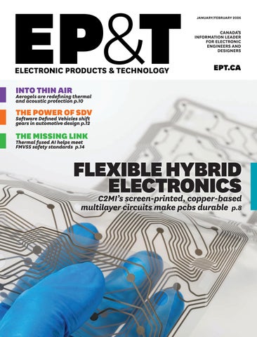
FLEXIBLE HYBRID ELECTRONICS

C2MI’s screen-printed, copper-based multilayer circuits make pcbs durable p.8

JANUARY/FEBRUARY 2026

STORY

4 EDITORIAL

Will 2026 bring us highs and lows?

7 WEST TECH REPORT ‘Femtech’ health device is AI enabled

8 THINK GREEN What to know about microplastics

In every issue

5 NEWSWATCH

18 NEW PRODUCTS

20 SUPPLY SIDE

21 AD INDEX

22 DEV BOARDS

Teledyne FLIR OEM Boson +IQ

8 GET TING FLEXIBLE IN DESIGN

Traditional printed circuit fabrication takes a back seat with C2MI’s screen-printed options.

10 ENGINEERING WITH AIR

State-of-the-art materials are being engineered into systems where failure is not an option.

12 MOBILITY SHIFTS GEARS

SDVs promise a new era of flexibility, efficiency and adaptability.

14 THE AI PERCEPTION STACK

The development path is significantly streamlined for car engineers integrating AI systems.

2026: A year of transition - and opportunity

As we turn the calendar to 2026, it’s clear that our industry stands at a meaningful inflection point.

The global electronics landscape continues to shift — not through a single disruptive moment, but via steady pressure from technology advances, market recalibration, and geopolitical realities. For Canadian innovators in design, engineering, manufacturing, and supply chain execution, the year ahead will require both resilience and strategic vision.

From a macro perspective, industry forecasts suggest that 2026 will be less about explosive growth and more about disciplined execution. After several years of expansion driven by AI acceleration, data-centre investment, and early consumer market rebounds, many traditional electronics segments are expected to grow modestly at best.

While AI server demand remains a bright spot, traditional end markets, such as smartphones, wearables and PCs, are expected to see minimal expansion, with wearable shipments potentially contracting.

That shift plays to Canada’s advantage. Across EP&T’s coverage through 2025, a common thread emerged: specialization matters. Growth continues in niche and high-impact markets such as AI-enabled embedded systems, advanced connectivity, industrial automation, medtech, and electrified transportation. These are areas where Canadian engineers excel.

One of the most encouraging signals heading into 2026 emerged from Accelerated: Canada’s Semiconductor Symposium, a two-day conference

held in Vancouver in late November. As reported, the event brought together leaders from industry, academia, start-ups, and government in an effort to define Canada’s role in the global semiconductor ecosystem. The message was clear: Canada is no longer content to be a quiet contributor. Instead, it is positioning itself as a strategic player — par ticularly in chip design, compound semiconductors, advanced packaging, photonics, and R&D-driven innovation.

For design engineers, this matters. The symposium reinforced that talent, IP creation, and system-level expertise are Canada’s strongest assets. While large-scale fabrication remains capital-intensive and globally concentrated, Canada’s opportunity lies in enabling technologies — designing the architectures, tools, and subsystems that make next-generation electronics possible. In 2026, expect increased collaboration between startups, research institutions, and multinational firms looking to tap into Canadian design exper tise.

Of course, opportunity does not arrive without friction. Cost pressures remain persistent across the electronics value chain. Materials pricing (affected by tariffs), labour availability, and logistics uncertainty continue to influence project timelines and margins. These realities elevate the importance of design-for-manufacturability, design-for-supply-chain, and lifecycle-aware engineering. Engineers are being asked to think beyond performance metrics alone, such as balancing cost, availability, sustainability, and long-term support from the earliest design stages.

Talent development is another defining issue. As highlighted repeatedly within our reporting through this past year, access to

skilled engineers and technologists remains a constraint on growth. This year, the industry’s success will increasingly depend on how well companies invest in training, mentorship and collaboration with post-secondary institutions. Encouragingly, industry initiatives point toward stronger national alignment, which would help ensure Canada’s next generation of engineers are equipped for semiconductor-centr ic and AI-driven design challenges.

Toolchains and workflows also continue to evolve. AI-assisted simulation, cloud-based EDA platforms, and collaborative design environments are becoming mainstream, enabling teams to manage rising system complexity with greater efficiency. For Canadian eng ineers working in distributed teams or across borders, these tools will be essential to staying competitive this year. Finally, we cannot overlook the broader geopolitical and trade environment. Supply chains remain under scrutiny, and nations are reassessing technology dependencies. In this context, Canada’s reputation for stability, technical excellence, and trusted partnerships is a strategic advantage. Electronics design done here increasingly influences products built and deployed around the world.

So, what’s in store for this year? It will likely be a year of measured momentum, where smart design decisions carry outsized impact, collaboration outweighs isolation, and innovation is defined by relevance rather than excess. For Canada’s electronics industry, the path forward remains challenging, but it is also clearly defined.

JANUARY/FEBRUARY 2026

Volume 48, Number 1

READER SERVICE

Print and digital subscription inquiries or changes, please contact Angelita Potal Tel: (416) 510-5113 Fax: (416) 510-6875

Email: apotal@annexbusinessmedia.com Mail: 111 Gordon Baker Rd., Suite 400 Toronto, ON M2H 3R1

EDITOR Stephen Law slaw@ept.ca · (416) 510-5208

WEST COAST CORRESPONDENT Mike Straus · mike@brandgesture.ca

BRAND MANAGER Joanna Malivoire jmalivoire@ept.ca · direct (416) 881-0731

ACCOUNT COORDINATOR Shannon Drumm sdrumm@annexbusinessmedia.com

MEDIA DESIGNER Curtis Martin cmartin@annexbusinessmedia.com

AUDIENCE DEVELOPMENT MANAGER Anita Madden amadden@annexbusinessmedia.com (416) 510-5183

GROUP PUBLISHER Paul Grossinger pgrossinger@annexbusinessmedia.com

CEO Scott Jamieson sjamieson@annesbusinessmedia.com

EP&T is published eight times per year by ANNEX BUSINESS MEDIA 111 Gordon Baker Road, Suite 400 Toronto, ON M2H 3R1 Tel (416) 442-5600 Fax (416) 510-5134 annexbusinessmedia.com

SUBSCRIPTION RATES

Canada – $62.06 one year; $99.72 two years USA – $142.15 (CAD) per year

International – $194.66 (CAD) per year Single copy – Canada $15.00

ISSN 0708-4366 (print)

ISSN 1923-3701 (digital)

PUB. MAIL AGREEMENT NO. 40065710 Return undeliverable Canadian addresses to: EP&T Circulation Department, 111 Gordon Baker Rd. Suite 400, Toronto, ON M2H 3R1

© 2026 EP&T. All rights reserved. Opinions expressed in this magazine are not necessarily those of the editor or the publisher. No liability is assumed for errors or omissions or validity of the claims in items reported. All advertising is subject to the publisher’s approval. Such approval does not imply any endorsement of the products or services advertised. Publisher reserves the right to refuse advertising that does not meet the standards of the publication. Occasionally, EP&T will mail information on behalf of industry-related groups whose products and services we believe may be of interest to you. If you prefer not to receive this information, please contact our circulation department.

PRINTED

NEWSWATCH

SEMICONDUCTORS

CANADA’S CHIP LEADERS CHART BOLD PATH

Canada’s semiconductor community recently gathered on the West Coast for Accelerated: Canada’s Semiconductor Symposium, a two-day event that reinforced both the momentum and urgency surrounding the country’s microelectronics ambitions.The event brought together industry executives, researchers, government officials and end-user sectors ranging from aerospace and automotive to medtech, mining, and advanced manufacturing.

Positioned as Canada’s signature semiconductor innovation event, the gathering offered a comprehensive look at the state of the national ecosystem and its role in global supply chains. Keynotes, panel discussions, and networking sessions explored how Canada can build a more resilient semiconductor supply chain, strengthen domestic design and manufacturing capacity, and advance next-generation technologies such as quantum, photonics, and microsystems. Attendees also toured advanced technical labs across the Vancouver region, providing a firsthand look at emerging research and commercialization activity.

FEDS SUPPORT CHIP PARTNERSHIP OF IBM CANADA, C2MI

The Federal Government has invested up to $210 million toward a $662 million project to expand semiconductor packaging and commercialization capabilities at IBM Canada’s Bromont f acility and the MiQro Innovation Collaborative Centre (C2MI), a microelectronics research and innovation centre.

The investment was made available through the Strategic Response Fund, and will bring new advanced packaging and R&D capabilities for next-generation semiconductors to Canada, while also helping Canadian companies accelerate commercialization of their products and supporting supply chain resiliency here at home. IBM will reportedly be able to develop and assemble more complex semiconductor packaging for transistors, which are applicable for moder n electronic devices.

“These projects are a major strategic step forward for C2MI and for

the entire semiconductor ecosystem in Quebec and across Canada. It can never be said enough: Semiconductors are ubiquitous in every economic sector and contribute to national advances in areas like artificial intelligence, quantum technologies and defence,” said said Marie-Josée Turgeon, CEO of C2MI. “Their manufacture is critical, and we will be able to play a strategic role in all areas while promoting the transition of our industry to a g reener and more competitive model.”

MEDTECH

BLOOD PRESSURE NECKBAND IS SELF-POWERED

A Vancouver researcher is being recognized for his groundbreaking work to design a first-of-its-kind self-powered continuous blood pressure (BP) monitor — a neckband with earphones — that provides measurements every few seconds. The breakthrough work has earned Dr. Tae-Ho Kim a Mitacs Outstanding Innovation Award.

Dr. Kim, a Simon Fraser University (SFU) postdoctoral fellow in the Biomechatronic Systems Laboratory, came up with the idea for a sensor-based neckband when dealing with his own hypertension. He noticed that his doctor had to spend extra time obtaining multiple BP readings using a traditional arm cuff device and thought there had to be a better way.

“It led me to ask research questions, such as if we could use small sensors to track how blood flows through the body instead of a cuff,” Dr. Kim said.

“Then I wondered, if such a device could be made, could we also make it more energy efficient, to be used anytime, anywhere?”

Kim went on to develop the novel neckband in conjunction with Medtronic, a global medtech leader that is working to advance hospital-at-home technologies in B.C.

“Through Mitacs, I was very fortunate to work with experts who helped me under stand market needs and guided me towards conducting more practical research,” he said.

ENGINEERING

QUILTER UNVEILS COMPUTER DESIGNED BY AI

Quilter, the physics-driven AI for electronics design, has unveiled a computer completely designed by artificial intelligence. A single engineer completed the layout taking a schematic to manuf acturing-ready files in less than a week, a process that traditionally takes an entire engineering team months and requires multiple rounds of redesign. This initiative, called Project Speedrun, represents a major milestone for the hardware industry, demonstrating an ability to compress quarter-long hardware R&D cycles into rapid weekly experiments.

Project Speedrun based its computer design around the widely used NXP i.MX 8M Mini processor, the same complex, embedded computing hardware commonly used in automotive infotainment, safety, and machine-vision systems. The system was fully functional upon first boot, capable of handling the demands of video calls, video games, and more – a rare outcome in printed circuit board (PCB) design, where projects typically build in as many as 3-5 respins when scoping.

“We see this as the compiler moment for hardware,” said Sergiy Nesterenko, CEO and founder of Quilter. “What used to take a team months now happens in days, which means you reach market months, if not a year, ahead of competitors.That’s how hardware will be built from now on.”

Canada’s Semiconductor Council held a conference in Vancouver this fall, involving senior players in the field.
Both IBM and C2MI received funding support from the Federal Government.
Dr. Tae-Ho Kim won a Mitacs innovation award for his selfpowered blood pressure neck monitor.

AI-enabled medical device aids women’s health

Vancouver-based Zero Candida Technologies begins prototype production, achieves design freeze

The femtech space is continuing to diversify beyond health tracking apps and software, with emerging hardware solutions offering women a variety of therapeutic products for women’s health concerns. One concern in particular, vulvo-vaginal candidiasis, has received attention from Vancouver-based startup Zero Candida Technologies, which is engineering an artificial intelligence-powered women’s health wearable for treating vulvo-vaginal candidiasis.

“Zero Candida’s device is the next gynecologist,” says CEO and founder Eli Ben Haroosh. “This device knows how to diagnose, treat, and transmit information to the doctor or patient in real time. In the future, our AI-powered device will know how to detect pregnancy, treat bleeding, and play a role in gynecological operations.”

Ben Haroosh says that 75% of women all over the world will suffer from vulvo-vaginal candidiasis at some point in their lives, making for a significant market for Zero Candida’s device. The device, coded ZC001, entered prototype production in October 2025, with an initial production run of 50 prototype units expected to be completed by Q1-2026. Z ero Candida’s ZC-001 is a nondrug, blue light therapy device that eliminates 99.9% of Candida fungus within 3 hours. Designed to resemble a tampon, ZC-001’s onboard smart computer uses an algorithm to assess the vaginal epithelium and adjust the blue light frequency as needed.

Onboard image sensor captures detailed

“Our technology works on a blue light wavelength with pulses of 410 nanometers, in a method unique to us, in which we kill the fungus with 99% success without harming other vaginal flora or probiotics,” Ben Haroosh explains.

ZC-001’s transparent gel matrix enables precise, localized drug delivery, which enhances efficiency while

Eli Ben Haroosh is the founder of Zero Candida Technologies in Vancouver, which develops ‘femtech’ devices to assist women’s health.

minimizing discomfor t. An onboard image sensor captures detailed visuals of the vaginal epithelium to provide a more accurate diagnosis, while a temperature sensor captures body temperature to assist in monitoring ovulation.

The device also features a pH sensor to detect pH imbalances, and a bleeding sensor to detect the presence of menstrual fluid with precision. ZC001 is designed in a tampon-like shape for ease of insertion and maximum comfort. The wearable technology even contains a Wi-Fi chip, enabling voice-over-IP connectivity and providing detailed information to healthcare professionals for consultations.

Zero Candida’s companion mobile app, which connects wirelessly to the device, enables users to collect and transmit treatment data to their physicians in real time, providing for constant monitoring and personalization.

Wireless connectivity enables encrypted data transfer

Zero Candida recently achieved a design freeze on its ZC-001 prototype. An initial production run o f 50 prototype units is underway, with completion expected by Q12026. “Achieving design freeze and starting prototype production marks a major advancement for

Zero Candida as we move closer to delivering a much-needed solution for women suffering from VVC,” said Ben-Haroosh in a press release.

The ZC-001 prototype design freeze includes design elements such as a docking system to provide for reliable charging and sterilization, wireless connectivity to enable encrypted data transfer, light-guide indicators to communicate device and charging status, and modular assembly to support scalable manufacturing. The prototype is made from medical-grade materials to ensure hygiene and long-ter m biocompatibility.

While Zero Candida’s current focus is on diagnosing and treating candida infections, the company aims to use its device to also provide analytics regarding pregnancy, bleeding, and other gynecological conditions.

The company completed a pilot trial in sheep in November 2023, and recently undertook a larger animal study in Q4-2025. Zero Candida is currently traded on three stock markets. Final results of the company’s preclinical studies are expected in Q1 2026, with the company aiming for U.S. clinical trials in 2027.

zero-candida.com

Mike Straus is EP&T’s West Coast correspondent. mike@brandgesture.ca

Photo: Zero Candida Technologies

Microplastics in electronics

What Canadian companies need to know in 2026

In 2026, microplastics (plastic particles smaller than five millimeters) are widely recognized not only as an environmental contaminant but also as a r egulatory concern for manufacturers whose products contain plastics. These particles move through ecosystems, enter food webs, and can interact with other contaminants; in aquatic organisms, their physical effects are now well documented. For Canadian electronics and technology manufacturers, this g rowing body of evidence has translated into concrete compliance obligations both domestically and internationally.

From enviro concern to regulatory reality

Historically, microplastics have emerged through two primary pathways: as incidental fragments produced as larger plastics degrade, and as intentionally m anufactured components incorporated into products. Plastics and composites are ubiquitous in the electronics sector, from housing, coating, and connectors to cable jackets and packaging. Consequently, many products contain materials that can generate microplastics through wear, abrasion, or end-of-life disposal.

Early regulator y action in Canada included the 2018 ban on microbeads in toiletries under the Canadian Environmental Protection Act (CEPA, 1999); this signaled that plastic byproducts were legitimate targets for policy. However, that ban addressed only a narrow subclass of intentionally added microplastics and did not extend to the broader material flows associated with manufactured goods.

The most immediate compliance obligation for Canadian manuf acturers today, including those in electronics, is the

Federal Plastics Registry. In 2024, Environment and Climate Change Canada issued a Notice under CEPA requiring companies that manufacture, import, or place plastic products on the Canadian market to beg in reporting detailed plastics data. Phase 1 reporting, due by September 29 last year, covered plastics in three categories:

• Plastic packag ing

• Plastic components in consumer electronic and electrical equipment

• Single-use or disposable plastic products

Entities that manufacture, import, or place more than 1,000 kg on the market per category annually must report quantities, resin types, and related lifecycle information, including how much plastic waste is generated, diverted, or disposed.

Phase 2 reporting, due by September 29, 2026, expands requirements to additional product categories, including all electrical and electronic equipment, for both professional and consumer use, while Phase 3 (2027) extends reporting into broader data domains.

Practical requirements

For electronics manufacturers, this translates into several practical requirements:

• Inventorying plastics in all products and packaging placed on the Canadian market

• Tracking resins and additives by weight and type

• Estimating end-of-life flows, including recycling, reuse, and disposal

• Implementing rob ust data systems ahead of current and upcoming reporting deadlines

Failure to report in a timely or accurate fashion may expose companies to enforcement action under CEPA.

Export

compliance:

EU REACH Annex XVII Canadian exporters must also contend with new European Union restrictions on microplastics. In 2023, the EU amended the REACH regulation through Commission Regulation (EU) 2023/2055, adding Entry 78 to Annex XVII. This measure restricts the placement of products containing intentionally added synthetic polymer microparticles on the EU market.

Main takeaways

Key provisions include:

• Applicability to polymers smaller than 5 mm, alongside certain insoluble, non-degradable fiber forms up to 15 mm in length

• A concentration threshold of 0.01 % (by weight) for intentionally added microplastics

• Phased compliance dates, with initial bans effective 17 October 2023 and additional obligations rolling out through the late 2020s

• Instr uctions of use and disposal with in-scope in vitro diagnostic devices.

• Repor ting and labelling requirements, including annual submissions to the European Chemicals Agency (ECHA) beginning in 2026 for specific use categories

For product designers and compliance teams, this entails:

• Assessing for mulations and components for intentionally added synthetic polymers

• Documenting polymer identities and functions for ECHA submissions

• Preparing required labelling or informational materials

• Evaluating alternatives or redesign options where materials fall within the restricted scope

Non-compliance can restrict access to the EU, one of the largest export destinations for Canadian technology products.

Steps for compliance

As regulatory expectations tighten, Canadian manufacturers should consider the following steps:

1. Audit all plastics in products and packaging, mapping quantities and resin types.

2. Engage supply-chain par tners to collect upstream data from resin suppliers and component manufacturers.

3 Develop data-tracking systems ahead of Federal Plastics Reg istry deadlines, including PLM or ERP integrations.

4. Review product designs for intentionally added microplastics that may trigger EU REACH restrictions.

5. Engage regulator y specialists for EU REACH submissions and labelling obligations.

6. Monitor evolving phase-in timelines for both Canadian and EU requirements.

Canada’s position and path forward

Canada’s regulatory posture on plastic, from domestic reporting to export-driven compliance, reflects a broader shift from environmental characterization to operational accountability.

The Federal Plastics Registry establishes a foundation for lifecycle transparency, while EU microplastics restrictions illustrate how environmental policy increasingly shapes product design and market access. For engineers, designers, and compliance professionals in the electronics sector, engaging early with these frameworks is no longer optional. It is an essential step in future-proofing products and supply chains as plastics regulations continue to evolve globally.

FHE materials bend the rules

C2MI advances flexible hybrid electronics with screen-printed copper-based multilayer circuit technology

JA. BENAVIDES-GUERRERO, LF. GERLEIN, K. SHAH, SG. CLOUTIER AT ÉTS; AND C. SANSREGRET, MJ. TURGEON AT C2MI

Traditional printed circuit fabrication has long relied on subtractive manufacturing techniques—most notably photolithog raphy and chemical etching—to define conductive pathways. While proven and precise, these processes depend on hazardous chemicals and generate substantial material waste, creating growing challenges for manufacturers facing stricter environmental regulations and sustainability mandates.

In response, additive manufacturing approaches—specifically sc reen-printed, copper-based circuitry—are emerging as a compelling alternative for Flexible Hybrid Electronics (FHE) production. FHE architectures integrate printed conductors on flexible or stretchable substrates with conventional surface-mounted components, enabling lightweight, mechanically compliant, and highly durable electronic systems. These attributes are unlocking new design freedoms and accelerating innovation across healthcare devices, consumer monitoring systems, automotive electronics, and IoT-enabled applications. Copper-based printing further expands integration possibilities by enabling electronics to be fabricated directly onto non-traditional substrates such as polymer s, textiles, and paper, while simplifying process flows toward scalable, cost-efficient manufacturing. Reflecting this momentum, forecasts from Grand View Research project FHE adoption to surpass US$54 billion by 2030.

Recent collaborative research conducted by École de technologie supérieure (ÉTS) in Montréal and

the MiQro Innovation Collaborative Centre (C2MI) in Bromont, Québec, demonstrates that screen-printed copper multilayer circuits can deliver electrical performance approaching that of bulk copper, while achieving excellent adhesion in compliance with ISO and ASTM standards. Reliability validation using JEDEC JESD22-A101 testing further confirmed the robustness of both singleand dual-layer printed circuits, with zero observed failures.

This article examines the current capabilities of multilayer screen-printed copper circuits, explores their target market applications, addresses remaining technical challenges, and outlines future development pathways—providing a comprehensive assessment of a manuf acturing paradigm poised to redefine flexible electronics integration.

Mechanical flexibility / environmental sustainability

Electronic manufacturing uses rigid substrates and subtractive processes. Screen-printed copper-based circuits open a wide range of new possibilities through cost-efficiency, mechanical flexibility and environmental sustainability. Emerging printed electronic solutions str ive to combine flexibility with multilayer sensing circuits, power systems and wireless communication modules to support a wide range of applications.

Multilayer screen-printed copper-based hybrid circuits offer key advantages including:

Form Factor Innovation through ultra-thin flexible FHEs, enabling integration of applications beyond

C2MI has responded to the growing pressures on electronic OEMs facing stricter environmental regulations and sustainability mandates.

traditional rigid electronics.

Direct Printing Integration atop a functional device or structures, without a separate substrate simplifying fabrication and lowering costs.

Cost-Effectiv e Deployment using additive processes reduces material waste by up to 90% compared to traditional methods.

Environmental Sustainability by minimizing toxic waste with the potential for using bio-sourced substrates alleviating environmental concerns associated with traditional electronics manufacturing.

Rapid Customization, using digital printing for rapid prototyping and application-specific designs for f aster time-to-market.

Distributed Intelligence using multilayer circuits to enable local signal processing using wireless communication for secure and embedded data handling.These improved capabilities represent a fundamental departure from traditional electronics, supporting the seamless integration of electronics into new everyday objects.

Screen-printed copper multilayer circuits

The fabrication includes:

1. Mesh preparation with appropriate count depending on ink rheology; 2. Stencil creation using photolithographic techniques;

3 Layer-by-layer deposit;

4. Ink application and squeegee-based transfer;

5. Controlled snap-off distance for optimal print quality; 6. Dr ying, curing, and sintering of printed layers.

For the assembly stage: Stencil preparation for solder paste deposition; and Component placement and reflow soldering. While screen-printing requires dedicated screens/stencils for each layer and design, limiting rapid prototyping capability, it facilitates the transfer to volume manufacturing of multilayer circuits.

The fabrication involves the following components:

Substrate Selection can include polyimide, FR4, and polyethylene terephthalate (PET), supplied by manufacturers such as Panasonic, Nomandy Coating, DuPont, and Polyonics. They must be cleaned and conditioned for optimal adhesion.

Polyimide (PI) provides excellent thermal stability with a glass transition temperature >300°C for ink sintering, excellent chemical resistance, superior mechanical strength and flexibility.

FR4 (Flame Retardant 4) is a cost-effective alternative offering good mechanical properties, thermal stability, and lower cost compared to specialty flexible substrates.

Ink Deposition using serigraphicor screen-printing involves transferring copper-based and dielectric inks through a patter ned mesh using a squeegee under controlled pressure and speed. Figure 4 shows the screen

patterned via photolithography to create the desired circuit patterns. Advanced manufacturing systems incorporate real-time alignment correction, crucial for multilayer architectures. Printing parameters are optimized to ensure uniform coverage and consistent linewidths. Successive layers are printed with precise alignment, enabling compact and complex circuit designs on flexible substrates

Copper-Based Inks offer good electrical performance, compatibility with standard copper-based processes and significant cost advantages over noble metals. Ink suppliers include ACI Materials, Celanese, Copprint, Creative Materials, Elantas, Henkel, Heraeus, Novacentrix, and VFP. Results show they can achieve conductivities close to that of bulk copper. Key characteristics include: 1- Particle size (0.1-10μm); 2- Copper content (65-75% by weight); 3- Viscosity (50–150 Pa·s); 4- Sintering profiles suitable for flexible substrates

Ink Additives can improve stability and performance. Additives include: 1- Defoaming agents to minimize bubbles; 2- Surface tension modifiers for ink spreading; 3- Antioxidants to prevent copper oxidation; 4- Unifor m particle sizes for packing. Other Conductive Materials to trade-off between performance and cost. They include: 1- Silver inks for higher conductivities; 2- Carbon inks for cost-reduction; 3-Hybrid formulations for tailored properties. Dielectrics for isolation between conductive layers, thermal stability to sustain sintering and mechanical flexibility. They include: 1- Printed polymers; 2- Laminated films between printed layers; 3- UV-curable inks for rapid low-temperature curing; 4-Organic-inorganic composites for superior mechanical and electrical properties. Cur ing and Sintering treatments using thermal or photonic processes are required for optimal performances. Multilayer Assembly involves robust alignment, material compatibility, and component attachment. The stacked architecture consists of:

1. Bottom copper layer (L1) for conductive pathways and pads for component integration; 2. Dielectr ic insulation layer; 3. A top copper layer (L2) for routing; 4. Via interconnects between copper layers;

Figure 1

Screen pattern design and printing.

Figure 2

Crosshatch test on screen printed copper. Demonstrator: printed copper on FR4.

Figure 3

Fully assembled and operational screen-printed multilayer copper circuit.

5. Solder paste for component placement.We use a low-temperature solder paste from Sn-Bi and a stencil.

Solder joint reliability and assembly characterization to ensure robust inter metallic bonding on printed copper, which is influenced by factors such as surface roughness for effective solder paste wetting. Encapsulation using glob-top materials like epoxy resins, silicones, or polyimides to alleviate corrosion and contamination while reinforcing adhesion and durability under flexion.

Enabling additive manufacturing

Compared to standard practices, the additive process reduces material waste, reduces process complexity, enhances environmental sustainability, and provides greater design flexibility to favor faster, cleaner, and more adaptable electronics manufacturing.

Pros and cons

Screen-printed copper multilayer circuits offer advantages and disadvantages when compared to traditional pcb manufacturing. Several challenges remain to fulfill the potential of screen-printed FHE circuits. Performance Limitations include higher resistance compared to bulk copper. Printing resolutions also limit the interconnect density and circuit designs. Process Control for consistent batch-to-batch performance over large areas requires outstanding control of ink viscosity, printing pressure, screen alignment, and sintering profiles. Integration Opportunities for practical implementations would ideally involve pr inting both conductive traces and some functional components through complementary processing techniques.

Screen-printed copper-based circuits for Flexible Hybrid Electronics (FHE) represent a paradigm shift in electronics manufacturing, offering a sustainable, cost-effective, and versatile alternative to traditional rigid systems

Authors: AC. Angel-Ospina, JA. BenavidesGuerrero, LF. Gerlein, K. Shah, and SG. Cloutier at École de Technologie Supérieure in Montreal; and C. Sansregret and MJ. Turgeon at C2MI, Centre de Collaboration MiQro Innovation, Bromont, QC. www.c2mi.ca

Engineering with air

How aerogels are redefining thermal and acoustic protection.

As electrification, space exploration, and high-performance computing push electronics into har sher, louder, and more thermally volatile environments, the materials protecting those systems are coming under new scr utiny. One material gaining renewed attention is aerogel—an ultra-light, nanoporous solid long admired for its extreme thermal and acoustic proper ties, but now finding broader commercial traction across modern electronic and electrical designs. From battery safety and cold-climate reliability to noise suppression and space-grade insulation, aerogels are emerging as a critical enabler for next-generation systems.

At the centre of this momentum in Canada is Acquire Industries. Based in Toronto, the company stands out as one of the country’s only suppliers and custom OEMs of aerogel insulation blankets, developing solutions tailored for demanding applications where conventional insulation falls short. Whether slowing thermal runaway in EV battery packs, stabilizing temperature-sensitive electronics in sub-zero industr ial enclosures, or protecting spacecraft components from extreme temperature swings and launch vibration, Acquire Industries’ aerogel technologies are being engineered into systems where failure is not an option. As demand for safer, quieter, and more energy-efficient electronic platforms accelerates, Acquire Industries is positioning aerogels not as exotic materials of the past, but as practical, production-ready solutions for today’s most advanced designs.

Thermal conductivities below 0.01

For readers who may only know aerogels from textbooks, these stateof-the-art materials are mostly made of silica, carbon, polymer, or hybrid variants - which start out as a sol-gel undergoing a supercritical drying process—engineered with porosities on the nanoscale exceeding 99%,

Acquire Industries has found success bridging the gap between curiosities and realities with its flexible aerogel blankets. This includes addressing markets beyond aerospace and defense.

densities as low as 3 mg/cm³, and thermal conductivities dipping below 0.01 W/mK, according to Edward Jerjian, P.Eng, CEO & principal engineer at Acquire Industries Ltd. While they’re still manufactured in monolithic form, the real gamechanger since their early discovery was overcoming their fragile nature by micronizing aerogels and turning them into dust.

“This made Aerogels more versatile, scalable, and capable of being integrated into composites and coatings while maintaining bulk properties and the inherent advantages of those nanoporous str uctures,” said Jerjian. “Advances in continuous fiber-spinning and supercritical CO₂ drying processes now produce flexible aerogel blankets and rigid panels at industr ial volumes. Engineers are mostly driven by this compulsion of achieving “impossible” performance in a whisper-thin lightweight profile. In electronics, that could mean squeezing R-10 insulation into a

5mm layer for EV battery packs or embedding conductive carbon aerogels as supercapacitor electrodes with 2,000m²/g surf ace area. They’re not just insulators anymore, but enablers in the next generation of electronics.”

Acquire Industries has found success bridging the gap between lab curiosities and realities. That also means addressing markets beyond aerospace, defense, and less notably oil & gas.The firm’s Flexible Aerogel Blankets have made their mark, and become far more accessible for building & construction applications, such as continuous insulation, thermal bridging and even heat trace systems, as well as industrial electronics by integrating them into electr ical equipment, including enclosures and cable trays.

Leverage aerogels into products or systems

“Our efforts to develop novel formulations or manufacture new aerogel materials stem from a core focus on

the “why”, as we leverage them in products or systems,” Jerjian offered. Think of Aerogels as the ‘Swiss Army knife’ of high-performance materials. Absolutely, ultra low-k grabs the headlines on the thermal side, but the real runway is in leveraging aerogels for lesser-known electrical, mechanical, and acoustic properties in advanced electronics design, according to Jerjian. Electrically, carbon and graphene aerogels have garnered attention with highly tunable resistivity as conductors rivaling carbon nanotubes for EMI shielding—absorbing >99% of waves up to 40GHz without reflection hotspots. They’ve also been developed as dielectrics with properties in the range of k~1.05 for low-loss RF substrates

“Mechanically, we’ve seen engineered compressive strengths over 100 kPa at 50% strain in flexible variants, for vibration-damped enclosures in drones or foldable sensor arrays in wearables,” said Jerjian. “Flammability is oftentimes overlooked, but many silica and hybrid aerogels are also inherently non-combustible, withstanding temperatures over 650°C and enabling UL 94 - V0 rated designs. Acoustically, their near-vacuum porosity slows sound propagation to under 300 m/s, attenuating airborne noise by up to 30-40 dB even in thin layers. We’ve worked on projects integrating Flexible Aerogel Blankets into anechoic chamber s and sound/ recording studios to cut distortion at high volumes. These aren’t just nice-to-have materials—they solve real pain points thermally, electrically, mechanically, acoustically, for flammability, and much more.”

Integ ration of aerogels is accelerating rapidly in automotive and EVs, as the firm is seeing massive uptake as battery thermal runaway barriers. Flexible aerogel blankets are being used to wrap cell modules, buying more than 10 minutes of containment time per GB 38031 and UL 2696 testing—with GM scaling to full packs. In aerospace, NASA continues to rely on silica aerogels in their Orion capsules and SpaceX’s avionics rely on aerogel-encased pcbs for radiation and cryo-insulation, surviving -200°C swings to re-entry heat.

“On the wearables and industrial electronics side it’s mostly theoretical and scientific discoveries driving attention,” noted Jerjian. “Flexible

and conductive aerogels have shown promise in sensors and e-skin for pressure, strain, or physiological monitoring, but these are not yet in commercial wearables. For Industrial Electronics, we might see them included in high-temperature potting and encapsulation compounds to slash convection losses within power modules and sensors in harsh environments.”

Jerjian says that aerogels are a top choice for passive thermal isolation, as their nanoporous structure traps air better than any foam, as low as k~0.01 vs. 0.025 for polyurethane. Eventually, they will excel in conformal, low-profile applications like gap fillers between stacked dies or chassis liners—as they can reach up to 5x better R-value per mm than graphite Thermal Interface Materials (TIMs).

“In EVs, aerogels outpace PhaseChange Materials (PCMs) by maintaining steady-state cooling without phase-shift latenc y, preventing hotspots in 800V architectures,” stated Jerjian. “In terms of shortcomings,

they’re not dynamic heat spreaders, since conductivity is very low at 0.02 W/m·K isotropic for lateral flow, so they would have to be hybridized with, for example, boron nitride.”

Yield stretchable electrodes for flexible batteries

Electronics could pay the premium if your folding phones are proving ROI via 15-20% energy savings, but you might have to budget for aerogels like you do copper foil. Right now, the market forecasts show the aerogels hitting $6B by 2035 at 16% CAGR, with economies from EV scale, according to Jerjian. That’s flexible aerogel blankets ramping up, with production increasing about 300% in 2024 alone.

“Broadly speaking on current-day cost barriers, it may be worth starting with manageable wins with integrations that leverage existing aerogel materials having already scaled,” he said.

From an R&D perspective, Jerjian calls conductive aerogels an exciting area right now. Doping with CNTs can yield stretchable electrodes for flexible batteries, hitting 1,000 mAh/g at 95% retention after 5,000 cycles. Hybrid composites, like nanowire/ graphene/aerogel/epoxy composites might achieve 0.5 W/m·K thermal conductivity with high electrical resistivity over 10^13 Ω·cm, possibly enabling electrically insulating TIMs for ther mal management in high-power electronics.

“While the science of various aerogels is giving birth to a new and emerging class of material, these lab discoveries are far from commercialization. The most exciting part is how aerogels are, and will be, integrated into products and systems engineered right now and in the future,” he stated. Where will aerogels make the biggest impact in electronic system design over the next five years? Jerjian is not entirely sure, but feels that there is certainly a runway for them to emerge as integral to many products and systems—much like we expected of graphene for decades.

“Looking ahead, engineers really need to upskill their understanding of how aerogels are poised to improve products, systems, and processes. They’ll need an eye on both material science and creative design thinking, working towards improving multiphysics simulations incorporating porosity effects,” Jerjian concluded.

Aerogels are designed to help engineers improve products, systems and processes.
Aerogels can be considered as the ‘army knife’ of high performance materials when designing new products.

The transformative power of software-defined vehicles

Mobility is undergoing a significant shift. Software-defined vehicles (SDV) promise a new era of flexibility, efficiency, and adaptability. But how can we navigate this change to ensure that new SDVs are not only innovative, but also safe and reliable? How can we integrate these vehicles into our digital lives in a way that meets our needs and expectations?

Software is at the heart of modern life, shaping how we work, connect, and experience the world. From the smartphones in our hands to the smart devices in our homes, software has transformed everyday objects into dynamic tools that can stay up-to-date with the latest features and services through over-the-air updates. This trend is now driving a profound shift also in the automotive world. Cars are no longer just mechanical machines; they are transforming into intelligent, connected platforms – better known as software-defined vehicles (SDVs).

With software at their core, these vehicles promise to deliver a new era of convenience, personalization, and performance that will redefine our relationship with mobility. With software-defined vehicles, this is now possible. This shift is turning cars into “computers on wheels,” unlocking endless possibilities for innovation.

For car manufacturers, software-defined vehicles open the door to new business opportunities. Instead of focusing solely on one-time sales, OEMs can generate fur ther revenue streams through software-enabled services and subscriptions. Features such as advanced driver assistance systems, premium infotainment options, or even performance upgrades can be offered as on-demand purchases. This approach not only enhances customer engagement but also provides automakers with valuable insights to improve products and services, turning cars into customer-centric platforms.

Automotive OEMs can generate further revenue streams through SDVs - such as ADAS and premium infotainment options.

The challenges of SDVs

However, the shift to software-defined vehicles introduces significant complexity that traditional electrical and electronic (E/E) architectures with a large number of electronic control units (ECUs) distributed in the car can no longer handle. This is why the automotive industry is transitioning to a more centralized approach with zonal architectures which divide the vehicle into physical zones – e.g. front, rear, left, and right – each managed by a powerful local controller. In addition, one or more central high-performance car computers are at the heart of the architecture. This approach reduces wiring complexity, improves communication efficiency, and simplifies updates, offering the scalability and modularity needed for SDVs.

Key features of a zonal E/E architecture:

• Modular ity: Zonal architectures allow for greater modularity, as different zones can be developed and upgraded independently.This modularity can lead to easier integration of new features and technologies.

• Flexibility: With the new architecture, a car’s electrical systems can be flexibly designed and adapted. New components and functions can be added or modified without affecting the entire vehicle architecture.

• Scalability: Vehicles are becoming

more complex with more and more electronic systems. With the scalability provided by a zonal approach, this increasing complexity can be managed more efficiently

• Reduced wire harness: By localizing components and controllers, a zonal architecture can reduce the amount of wiring required in a vehicle, resulting in lighter and more efficient designs.

• Faster development and updates: A zonal architecture enables faster development cycles and easier software updates since changes in one zone may not necessarily require changes to the entire system.

• Improved reliability and redundancy: Critical functions can be distributed across different zones in the new architecture. This reduces the impact of a single point of failure, improving reliability and redundancy.

How semiconductors shape SDVs

Zonal architectures rely on advanced semiconductors to bring SDVs to life. They require powerful microcontrollers (MCUs) or system-on-chips (SoCs) to handle the simultaneous processing of multiple vehicle functions while enabling seamless, high-speed communication through advanced protocols like Ethernet. Functional safety and cybersecurity are equally critical considerations.With SDVs relying heavily on connected systems and cloud interactions, protecting sensitive data and preventing cyberattacks are top priorities. Zonal architectures demand semiconductors with integrated security features that can detect anomalies, safeguard against threats, and alert drivers in case of potential breaches. A scalable, layered security framework – including encryption, real-time monitoring, and compliance with global automotive cybersecurity standards – is vital to ensure that vehicles remain safe, even as software evolves over time.

Photo: Blue Planet Studio / Getty Images

Advanced Magnetics for ADAS

From high-current, high-efficiency power inductors to filter components for a variety of communications buses, Coilcraft has the magnetics for all of your Advanced Driver Assistance Systems

Coilcraft offers a wide range of AEC-Q200 qualified products engineered for the latest advanced driver assistance systems, including high-temp, high-power-density, power inductors for radar, camera and LiDAR applications.

Our compact Power over Coax solutions offer significant board-space savings while providing the high signal performance

needed for today’s high-resolution and highspeed cameras.

Also choose from our broad selection of common mode chokes and filter elements for a variety of communications buses.

To learn more about our advanced solutions for ADAS and other automotive/ high-temp applications, visit us at: www.coilcraft.com /AEC

Thermal-fused AI

The missing

link in meeting 100% pass

rate for FMVSS No. 127’s. BY CHRIS POSCH, TELEDYNE FLIR OEM

Here are several troubling statistics. The Governors Highway Safety Association (GHSA) states that more than three-quarters of pedestrian fatalities occur after dark. Between 2010 and 2023, the number of fatal nighttime pedestrian crashes rose 84%, compared to a 28% increase in daytime fatalities for the same period. When the National Highway Traffic Safety Administration (NHTSA) tested five production vehicles’ nighttime Pedestrian Automatic Emergency Braking (PAEB) systems in 2023, four out of five failed at least two test scenarios, with only the 2023 Toyota Corolla Hybrid passing all tests of what would become the required standard for Federal Motor Vehicle Safety Standard (FMVSS) No. 127.

There’s a clear increase in global awareness of road safety. Whether in the news, on social media, or with government representatives passing new automotive standards, more vehicles are being equipped with Advanced

Driver Assistance Systems (ADAS) features, and a number of metropolitan areas are seeing fully autonomous vehicles such as robotaxis from Waymo and Zoox.

While Transport Canada’s Canada Motor Vehicle Safety Standards (CMVSS) does not yet include a mandatory standard for PAEB, the 2024 U.S. FMVSS No. 127 mandates that PAEB systems on new vehicles weighing 10,000 lbs. Gross Vehicle Weight (GVW) or less achieve a 100% pass rate by September 2029, and with momentum from one region potentially influencing another, Canadian standards may follow in the future.

Critical challenge

Automotive manufacturers face a critical challenge: existing PAEB sensor suites that include cameras or cameras and radar aren’t cutting it. One solution is to add a thermal camera to the existing ADAS sensor suite to create thermal-fused PAEB.

FMVSS No. 127 requires a 100% pass rate for detecting

pedestrians in both daytime and nighttime lighting conditions and at new, increased vehicle speeds. For engineers developing ADAS sensor suites, there’s a technical imperative: leverage sensor redundancy that performs reliably when visible cameras underperform in darkness.

In September 2024, testing by VSI Labs validated the effectiveness of a thermal-fused PAEB system in three new 2024 commercial-off-the-shelf (COTS) vehicles with state-ofthe-art PAEB technology. Only the thermal-fused PAEB system passed all nighttime FMVSS No. 127 tests. The COTS vehicles all failed at least one nighttime test scenario. The underlying reason is straightforward: visible cameras are limited by headlight illumination, even with high-performance image processing techniques, and radar does not provide adequate high-resolution data.

Thermal-fused PAEB integrates a longwave infrared (LWIR) thermal camera with a standard automotive visible

camera and radar and processes them through advanced perception models. The key differentiator is that an LWIR thermal camera operates in the eight to 14-micron wavelength range, passively detecting infrared energy, commonly known as heat, rather than relying on reflected visible light.

Performance advantages are compelling

This is not a simple incremental improvement; it’s orthogonal sensing that requires no active illumination. Since all objects emit or reflect thermal energy, the system provides both redundancy and greater situational awareness for the vehicle.

The performance advantages are compelling, especially at night, as thermal cameras see significantly farther beyond the headlight illumination, providing advanced warning that’s crucial for heavier vehicles requiring longer braking distances, cluttered urban environments, and r ural roads with limited to zero illumination. Automotive Safety Integrity Level (ASIL)-B-compliant LWIR camera modules c an discern temperature differences as small as 50 millikelvins (mK) (0.05°C), with 640×512-resolution delivering

Figure 1. GHSA Pedestrian Fatality Data
Figure 2a/b. Teledyne FLIR OEM automotive thermal LWIR camera (above) and fused visible-thermal perception output from Prism AI (below).
Photos: Teledyne Flir OEM

long-range pedestrian detection.

The AI perception stack:

The computational engine that interprets fused sensor data typically leverages convolutional neural networks (CNNs). Perception frameworks such as Prism AI Auto software analyze thermal data in real time for classification, object detection, and tracking.

For engineers integrating these systems, the development path is significantly streamlined. Existing training datasets accelerate deployment with millions of thermal annotations combined with AI-optimized frameworks. The technical architecture addresses both detection and classification, with the thermal modality dramatically improving reliability for partially obscured targets like pedestrians darting from behind vehicles or par tially hidden by foliage.

Engineering specifications that matter

Functional safety isn’t optional. It requires components such as ASILB-rated thermal LWIR cameras that comply with ISO 26262 functional safety standards.

Key engineering features include a shutterless design for maximized uptime (no momentary video pipeline freeze), power efficiency, and affordability, plus heated IP6K9K enclosures that ensure reliable 24/7/365 all-weather operation. These aren’t luxury specifications—they’re engineering necessities for systems for which failure isn’t acceptable.

From ‘too expensive’ to ‘can’t afford not to’

The economics of thermal integration

have fundamentally shifted. Volume production, improvements in pixel geometry, and centralized automotive compute have made thermal cameras viable for mass-market deployment. For OEMs, the calculation is straightforward: the cost of integrating a robust thermal camera is significantly lower than the potential of failing to comply with FMVSS No. 127 or, worse, preventable fatalities.

Solving Corner Cases

Regulatory compliance is the baseline. The harder problems are the corner cases—complex, unpredictable real-world situations are potentially more challenging than test protocols. Standard ADAS sensor suites str uggle with pedestrians in dark clothing against dark backgrounds, partially occluded vulnerable road users, wildlife on rural highways, dense fog or smoke conditions, and rapid transitions from bright to dark environments.

Thermal fusion provides redundancy and robust performance in adverse conditions that are non-negotiable for higher SAE automation. An extended detection range and reliable classification of living creatures ensure more comfor table, safer deceleration, improving both the passenger experience and crash avoidance.

For electronics designers and engineers developing next-generation

3. Side-byside visible camera and thermal camera video frame captures from the VSI research vehicle during a low-beam stationary test at approximately 45, 35, 25, and 15 meters.

vehicular platforms, thermal-fused PAEB integration follows a clear technical path: select ASIL-B compliant ther mal sensors meeting ISO 26262 functional safety standards, integrate perception frameworks leveraging pretrained thermal datasets, implement sensor fusion algorithms combining LWIR, visible, and radar data streams, validate against FMVSS No. 127 protocols plus corner case scenarios, and design for automotive environmental robustness including temperature, vibration, weather, and moisture considerations.

The availability of annotated thermal image datasets and perception software tools simplifies machine learning model development, which previously represented a significant engineering barrier.

Vision zero

FMVSS No. 127 represents a pivotal inflection point. While Transport Canada has yet to issue its own ruling, it has been studying AEB technologies and collecting feedback to evaluate best practices. Meeting FMVSS No. 127 with the conventional COTS sensor suite has proven difficult. The data from NHTSA testing and independent validation demonstrate that thermal-fused PAEB isn’t just an enhancement; it’s the logical path forward for engineers designing robust, reliable perception systems.

Figure
Figure 4. Automotive thermal IR cameras see infrared energy (heat) at 8 to 14 microns

August Electronics maps out new playbook

Following the acquisition by India-based Kaynes, Calgary CEM details how expanded resources and global expertise will drive its next phase

When Calgary-based August Electronics Inc. was acquired in May 2025 by Kaynes Canada Ltd., a wholly owned step-down subsidiary of Kaynes Technology, an India-based electronics system design and manufacturing (ESDM) powerhouse - it marked a significant shift for one of Western Canada’s leading contract electronics manufacturers (CEM). For many in Canada’s electronics sector, the deal signaled both opportunity and uncertainty: What would it mean for August’s long-established identity? And how would its operations and customer relationships evolve under new international ownership?

To unpack these questions, EP&T Magazine sat down with Paul Crawford, an advisor supporting August Electronics dur ing its transition period. In a wide-ranging discussion, Crawford outlined the strategic implications of the acquisition, from the expected boost to August’s manufacturing and engineering capabilities to the realities of maintaining business continuity through existing leadership. He also addressed the difficult questions - whether the company’s customer mix or contract profile might shift, and how August plans to balance local autonomy with integration into a global technology group.

What follows is an inside look at how August Electronics intends to navigate this pivotal moment, and what the Kaynes Technology partnership may mean for Canada’s electronics manufacturing landscape. As par t of the transition, co-founders Jack Francis and Peter Wilson have stepped away from their roles. CEO Tanya Korenda remains at the helm, ensuring continuity as the company enters its next chapter. Korenda’s ongoing

Paul Crawford of August Electronics sits down with EP&T to discuss the impact of the recent acquisition of the Calgary-based CEM by India-based Kaynes Technology, a ESDM powerhouse.

commitment to August, paired with the continuity of its established management team, ensures the transition has little impact on employees or dayto-day operations. Instead, the change opens new pathways for expansion, positioning August to deliver a distinct and strengthened value proposition to the market.

Identity and operations

Kaynes currently operates nine locations across India and one in the U.S. (Digicom). According to Crawford, the company’s goal was to find a North American hub capable of serving as the headquarters for regional expansion. With existing customers in South Asia and Europe, Kaynes sought a sizeable, established

operation like August Electronics to anchor its Western growth strategy.

“It was never about getting the customers and then taking their business to India,” Crawford said. “It was about growing Kaynes’ footprint worldwide, starting in North America. They wanted to keep all the people and expand—which means opportunity for everybody.”

August’s Calgary facility is expected to operate as the North American “hub,” with further CEM growth driven organically and through future acquisitions.

Senior executives from both organizations have completed multiple site visits to better understand one another’s operations. Crawford and CEO Tanya Korenda toured Kaynes’

Paul Crawford has served as an advisor supporting August Electronics through its acquistion transistion with Kaynes.

Leveraging its new ownership, Calgarybased CEM August Electronics sets out to boost its engineering and manufacturing capabilities.

Indian facilities earlier this year.

“One significant difference between our market and Kaynes is their access to cost-effective labour,” Crawford said. “If a problem arises, they can solve it quickly by putting more people on it. Their processes—particularly in material receipt and verification— are exceptional. We were blown away by the cleanliness, thoroughness, and efficiency.”

Enhancing capabilities

The acquisition will soon give August Electronics direct access to several production services it currently outsources. Kaynes’ expansion in India includes electronics design engineering, bare printed circuit board (pcb) fabrication, injection moulding, plastics, cabling, and sheet metal operations.

“This will support August’s customers who are seeking lower-cost supply for these services,” Crawford said. “Going abroad often raises questions about quality, but our Calgary facility will stand fully behind the work with our own internal quality checks.”

Concerns about preserving August’s “Canadian DNA” were quickly addressed.

“They want a functioning, independently operating company,” Crawford said. “They’re not looking to impose their culture on August or make sweeping changes. And if August needs financial support for organic or inorganic growth, we now have access to the capital to do that.”

The new ownership model will also influence the types of contracts and customers August pursues.

“Kaynes works with many multinational OEMs around the world, including organizations with operations in Canada and the U.S. That immediately gives August Electronics a new pathway,” he explained. “Existing customers will benefit from upgraded technical capabilities and the option to run larger-volume production in India.”

August has long built a strong reputation in high-mix, low-volume manufacturing

with a focus on medical, aerospace, defence, and data centre sectors. According to Crawford, that focus isn’t changing.

“Kaynes was particularly interested in our relationship with Alberta’s oil, gas, and energy markets,” he said. “Some firms hesitate to associate themselves with those sectors due to environmental optics.”

The acquisition also introduces new “dual-shoring” opportunities for customers,

offering both Canadian and India-based production routes.

“Kaynes wants to use August as a vehicle for growth in Canada and North America,” Crawford said. “It presents opportunities for our customers and great opportunities for our staff—and for people entering this industry. Customers will continue receiving the quality and service they expect from August, but now we’ve got more tools in our toolbox.”

To Be Creative

Strip Series B300

Powerful, Efficient, and Intuitive Stripping Machine

Schleuniger’s portable Strip Series B300 delivers fast and reliable stripping of wires with crosssections from 32 to 8 AWG. The machine‘s ergonomic design and intuitive user interface offer unrivaled ease of use, while repeat accuracy, mechanical precision, and short process cycles ensure maximum productivity.

„ Compact modular design

„ High-resolution 5” color touch screen

„ LED lighting for clear view of work area

„ Highly sensitive trigger mechanism

„ High process reliability

Wire Solutions for a Connected World schleuniger.com 905-827-1166

ANALOG I/O LINE DELIVERS 4-20MA CURRENT FOR EMBEDDED SYSTEMS ACCES I/O PRODUCTS

DAAI16-8F high-performance PCI

Express Mini Card (mPCIe) multifunction analog output/input module delivers 16-bit precision, simultaneous analog output and input and flexible digital I/O in a small, rugged design suitable for embedded and OEM applications. Product integrates eight 16 bit analog outputs supporting both voltage and current outputs, serving applications that need 4-20mA control.

www.accesio.com/product/ mpcie-daai16-8f/

COMPACT AC-DC DIN RAIL POWER SUPPLIES ARE ‘INTELLIGENT’

MEAN WELL

Single-phase XDR-E and three-phase XTR series compact, intelligent and high-efficiency ac-dc DIN rail power supplies feature several upgrades designed to deliver high-reliability performance in many applications. Products feature slimmer form factors, which improve control panel design flexibility and space efficiency. Units deliver higher efficiency performance, which reduces energy consumption and heat production. Products provide lower inrush current, mitigating electrical disturbances. www.meanwell.com

ALUMINIUM

ENCLOSURES MEET A

WIDE RANGE OF APPLICATIONS

BOPLA

Aluminium enclosure types combine sturdy construction with environmental protection up to IP69. Products stand out in market simple or elegant designs, available in a wide range of sizes, offering flexible equipment housings. All empty aluminium enclosures can be finished individually, using processes such as coating, laser marking or printing and a full custom design service is available.

https://www.bopla.de/en

MINIATURE SMT TEST POINT FEATURES

SYMMETRICAL

FLAT-WIRE DESIGN

EMX ENTERPRISES

Keystone Electronics Miniature SMT Test Point features a symmetrical flat-wire design to efficiently and safely test pcbs. This ‘Mini’ version enables high-strength, test point-to-pcb bonding, with a minimal footprint. Product accepts a variety of gripping probes to replace wire-wrap posts and turret terminals - suitable for testing circuitry of high-density pcb packages. Product is manufactured from silver-plated phosphor bronze for both lead-free solder and traditional reflow processing - compatible with most vacuum and mechanical pick-and-place assembly systems. www.emx.ca/

SILICONE PASSES NON-CYTOTOXICITY STANDARDS

MASTER BOND

MasterSil 800Med one component, moisture curing silicone is specifically designed for medical device manufacturing, as it passes ISO 10993-5 testing for non-cytotoxicity. The material is non-corrosive and possesses enhanced flow properties, improving general bonding, sealing, coating and form-in-place gasketing. Compound is black in colour and delivers high resistance to dry heat and sterilization methods. Product cures very quickly upon exposure to atmospheric moisture or humidity. www.masterbond.com/ products/silicones-medicaldevices

COMPACT, ROBUST, WATERTIGHT CONNECTORS ARE RESIN-FREE LEMO

REDEL SP IP68 Series next generation of high-performance connectors are engineered for medical, test & measurement and UAV applications. Devices combine resin-free IP68 sealing with firm’s patented ‘push-pull’ system and high-density design, making devices that are reliable, easy to use, and fully compliant with the strictest medical and industrial standards. Product delivers fully watertight and dustproof performance without the need for resin or potting, simplifying assembly, ensuring compliance, and maintaining high reliability even in the most demanding environments. www.lemo.com/en/solutions/ highlights/redel-sp-ip68-series

LOW-VOLTAGE BLUETOOTH LE SOC SERVES NEXT-GEN HEALTH WEARABLES

NORDIC SEMICONDUCTOR

nRF54LV10A SoC sets a new benchmark for integration, performance and battery life in the smallest medical devices. Engineered for space-constrained, low-voltage Bluetooth LE applications, device can be powered directly by a single silver oxide coin cell making it suitable for wearable biosensors, continuous glucose monitors (CGMs), and other healthcare applications. Device is the fifth addition to firm’s next generation nRF54L Series of wireless SoCs, providing a fit-for-purpose feature set for applications demanding ultra-low power consumption and reliable connectivity in the most compact form factor possible. This includes support for 1.2-1.7 V supply voltage range, a sub-50 nA system hibernation mode for shipping and storage, and an ultra-compact 1.9 by 2.3 mm chip-scale package, the smallest available in the nRF54L Series.

https://www.nordicsemi.com/ Products/nRF54LV10A

SIC MOSFETS IN TOLL PACKAGE ACHIEVE MINIATURIZATION, HIGH-POWER CAPABILITY ROHM

SCT40xxDLL series of SiC MOSFETs in TOLL (TO-Leadless) packages provide approximately 39% improved thermal performance compared to conventional packages (TO-263-7L) with equivalent voltage ratings and on-resistance. This enables high-power handling despite their compact size and low profile. Suitable for industrial equipment such as server power supplies and ESS (Energy Storage Systems), product reduces component footprint by approximately 26% and achieves a low profile of 2.3mm thickness. Device supports a drain-source rated up to a voltage of 750V.

www.rohm.com/products/ sic-power-devices

RUGGED, MULTI-PORT SMPM INTERCONNECTS

DELIVER THREADED COUPLING

SAMTEC

Magnum RF line of rugged, multi-port SMPM solutions feature threaded coupling for high thermal shock and vibration environments commonly found in military, aerospace and communication applications. Devices provide high-frequency performance up to 65GHz with enhanced reliability in high-density applications. SMPM multi-port mated sets with the new -S Screw option for threaded coupling are part of the product line. Cable assemblies are available with .047” diameter low-loss flexible cable (GC47 Series) or with .086” diameter low-loss flexible cable (GC86 Series). www.samtec.com/rf/original/ magnum/

HANDHELD ANALYZER

ENABLES

120-MHZ IQ STREAMING

KEYSIGHT TECHNOLOGIES

N99xxD-Series FieldFox Handheld Analyzer is purpose-built for precision and portability, enabling 120MHz gap-free IQ streaming, high-speed data transfer and seamless field-to-lab integration, creating a benchmark for wideband signal analysis in demanding RF environments. Product series combines the ruggedness of a field instrument with the power and precision of a lab analyzer. It empowers users to capture, stream and replay every signal event, enabling faster troubleshooting, deeper analysis, and greater confidence that no data is missed. www.keysight.com/

CHIP PERMITS ADDED LIGHTING, ACCESS CONTROL, SECURITY TO IOT DEVICES

STMICROELECTRONICS

ST25DA-C secure NFC chip is designed to make home networks faster and easier to install and scale, leveraging the latest Matter smarthome standard. Chip lets users add lighting, access control, security cameras, or any IoT device to their home network in one step by tapping their phone.

Type 4 chip improves the user experience, leveraging NFC technology present in most smartphone devices. NFC tag can operate cryptographic operations required for Matter device commissioning. https://www.st.com/content/ st_com/en

COLD-FORGED PIN-FIN IC COOLER DELIVERS ULTRA-THIN STANDARD

JARO THERMAL

Cold-Forged Pin-Fin IC Coolers feature a cold-forged pin-fin heatsink core paired with a high-performance fan for enhanced thermal management. Built using next-gen cold-forging metallurgy and fine-pitch pin-fin design, the result is an improved thermal performance in a compact 13mm profile. The ultra-thin IC coolers are available with aluminum and copper options, maximizing surface area for efficient heat dissipation. https://jarothermal.com/2025/05/ 27/compact-size-colossal-coolingjaros-cold-forged-pin-fin-ic-coolerdefines-the-ultra-thin-standard/

WHEN EVERY PART MATTERS, SO DOES THE SOURCE.

Don’t risk purchasing on the gray market. Rochester provides a continuous source of supply for applications where the product lifecycle extends beyond the active availability of a device. Our factory-direct offering negates the need for expensive testing. We keep businesses moving with 100% authorized, traceable, certified, and guaranteed devices.

Creations Technologies’ 154,000 sq. ft. manufacturing facility in Rochester, NY. Image

CEM

CREATION MARKS 35 YEARS OF EMS SERVICES

Contract electronics manufacturer Creation Technologies is marking 35 years of supporting original equipment manufacturers (OEMs) with engineering, prototyping , manufacturing, supply chain, and fulfillment solutions. Since its founding in 1991, the company has grown to more than 3,200 employees and operates 13 manufacturing facilities across the United States, Canada, Mexico and China.

Creation partners with customers in the aerospace & defense, medical and Industrial technology segments, providing services that span the entire product lifecycle from initial engineering design and rapid prototyping through production and after market support. Its facilities are optimized to handle complex electronics assemblies, system integration, wire and cable harnesses, testing and logistics.

SYNTRONIC EXPANDS MANUFACTURING OPERATIONS IN ONTARIO

Syntronic is expanding its manufacturing operations in Ottawa with a move into new premises at 340 Legget Drive in the Kanata North Research Park. The expansion brings a major increase in capacity and capability, consolidating production and repair operations under one roof and more than doubling total floor

space to approximately 70,000 square feet.

The new location is less than five minutes from Syntronic’s local R&D site, tightening collaboration across the entire product lifecycle from design to full scale production. The proximity strengthens the company’s integ rated approach, where engineering and manufacturing teams work closely together to accelerate innovation and maintain the highest standards of quality.

Syntronic’s new location is less than five minutes from its local R&D site.

“Syntronic’s strength has always been our ability to adapt and grow alongside our customers,” said Björn Jansson, Founder and CEO of Syntronic Group. “Expanding our manufacturing presence in Canada is another step in that journey, ensuring we can meet future needs with the same innovation, quality, and customer focus that define Syntronic globally.”

BITTELE RENEWS ISO 9001:2015

Bittele Electronics has renewed its ISO 9001:2015 certification for its turnkey printed circuit board (pcb) assembly services in

Markham ON. Bittele has held ISO status since January 2020, demonstrating ongoing compliance across multiple audit cycles. ISO 9001:2015 validates process control, risk management, supplier oversight, and continuous improvement.

“This isn’t a vanity exercise,” said Bittele CEO BenYang. “ISO forces discipline—real documentation, corrective action, and operational accountability.”

DISTRIBUTION

FUTURE OPENS DOORS AT NEW MONTREAL HQ

Global electronic components distributor Future Electronics has officially moved into its new headquarters in the Montreal area this week, marking a significant milestone in the company’s g rowth and long-term presence in Canada. The relocation brings together employees from across departments into a modern workspace designed to support collaboration, innovation, and the company’s expanding global operations.

The grand opening earlier this week featured internal celebrations, including team gatherings and welcome events for staff, underscoring the company’s commitment to community and employee engagement as it embarks on this next chapter. The new headquarters will serve as a central hub for Future Electronics’ worldwide supply chain, engineering, and business functions.

Founded in Montreal in 1968 and now operating in more than 40 countries, Future Electronics seeks to continue building on its legacy as a leader in the electronics distribution industry.

DIGIKEY DEBUTS POWER SUPPLY CONFIGURATION TOOL

DigiKey has introduced its power supply configuration tool, which simplifies the process of designing power supply solutions. Developed for engineers, designers and system integrators,

DigiKey’s power supply configuration tool simplifies the design of power solutions.

this intuitive online tool enables the quick selection of key attributes—such as outputs, voltage, cur rent and more—to generate a tailored power supply solution that meets users’ desired requirements. Once configured, the custom power supply is assembled and shipped directly within days . Hosted on DigiKey’s trusted, high-performance website, the configurator enables f ast and accurate selection and sourcing—making it easier than ever to design, customize and order the right power solution for the project.

INDUSTRIAL AUTOMATION

SIEMENS, NVIDIA EXPAND PARTNERSHIP

Siemens and NVIDIA announced a significant expansion of their strategic partnership to bring artificial intelligence into the real world. Together, the companies aim to develop industrial and physical AI solutions that will bring AI-driven inno vation to every industry and industrial workflow, as well as accelerate each others’ operations.

To support development, NVIDIA will provide AI infrastructure, simulation libraries, models, frameworks and bluepr ints, while Siemens will commit hundreds of industrial AI experts and leading hardware and software.

DEVELOPMENT BOARDS

Thermal imaging hardware and software development kit

VENDOR: TELEDYNE FLIR OEM

BOSON+ IQ DEVELOPMENT KIT

Teledyne FLIR OEM hardware and software development kit accelerates thermal imaging and AI integration at the Edge. The comprehensive solution combines reference hardware with Prism software, empowering integrators to rapidly develop edge AI capabilities using advanced thermal sensing across defense, security and industrial platforms.

At the heart of the kit is the Teledyne FLIR OEM AVP, powered by the Qualcomm Dragonwing QCS8550 system-on-chip (SoC), which delivers an industry-leading 50 trillion operations per second (TOPS) with a typical power draw of 2.5 watts. Its multicore architecture supports Prism AI object detection models and Prism ISP features, including denoising and super resolution to provide exceptional image clarity in challenging environments.

Specs

Imaging and Optical

• 640 x 512 / 30Hz (typical) to 60Hz (configuration dependent)

Frame Size / Rates

1280 x 1024 w/ Super Resolution / 30Hz (typical) to 60Hz (configuration dependent)

Pixel Pitch

• 12 µm

Resolution

Boson+ 640x512 (32° HFOV) w/ shutter

Designed for flexibility and scalability, the kit includes interface and carrier boards with three MIPI interfaces, allowing developers to integrate visible or other sensor types into their systems. It also comes with the Boson+ and Prism SDKs, hardware interface control documentation (ICD), and expert engineering support, providing a seamless development experience from prototype to deployment.

The Boson+ IQ Development Kit is future-ready, with compatibility for upcoming additions, including Prism SKR and Prism Supervisor. Prism SKR facilitates autonomous target detection and terminal guidance, while Prism Supervisor offers autonomous operation to designated way points via GPS or visual-based navigation (VBN) location technology.

These software-enabled features can add powerful capabilities to mission-critical applications in defense, security, and industrial automation.

The Boson+ IQ Development Kit enables integrators to evaluate and develop thermal infrared (IR) sensing with AI object detection and image signal processing (ISP) at the edge.

Develop on the Qualcomm Dragonwing QCS8550 platform, as the processor enables extreme edge AI at low power.

Boson Plus 640 CZ, 14-75 is a continuous zoom lens version of the Boson+, serving as an option to add if you design needs call for it.

Scan here to view and download the full data sheet in pdf format.

Photos: Teledyne Flir OEM

Hammond has over $30 million of in-stock inventory and over 16,000 unique product skus to choose from.

WE ARE IN-STOCK

At Hammond, we are proud of our Canadian roots. We manufacture in Canada, we warehouse in Canada, and we employee over 900 Canadians. We are Canada’s Enclosure Company.

Turn static files into dynamic content formats.

Create a flipbook
Issuu converts static files into: digital portfolios, online yearbooks, online catalogs, digital photo albums and more. Sign up and create your flipbook.