The next discovery is at hand
Unearth millions of components for your next design













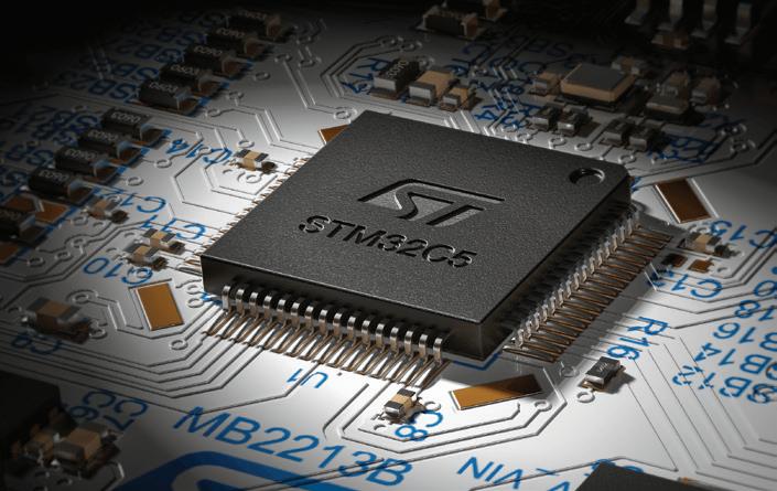


The next discovery is at hand
Unearth millions of components for your next design
Access to the latest semiconductors and electronic components remains a critical challenge for engineers, particularly when working with emerging technologies where early access can shape design decisions and speed to market. Mouser Electronics addresses this need through its New Product Introduction (NPI) strategy, enabling engineers to evaluate and adopt new technologies earlier in the development process.
Backed by a highly automated global logistics network, Mouser offers more than 6.8 million components from over 1200 manufacturers to customers worldwide. As an authorised distributor, the company provides genuine, fully traceable products through manufacturer-authorised channels, with no minimum order quantities to support prototyping and testing. Australian customers benefit from in-stock online delivery typically within three to four days, supported by a dedicated local customer service centre offering assistance in local language and during local business hours. Combined with continued investment in digital tools and online platforms, Mouser helps engineers streamline development and bring innovative ideas to market more efficiently.

Westwick-Farrow Media
A.B.N. 22 152 305 336
www.wfmedia.com.au
Head Office
Unit 5, 6-8 Byfield Street, North Ryde Locked Bag 2226, North Ryde BC NSW 1670 Ph: +61 2 9168 2500
Editor Ashna Mehta wnie@wfmedia.com.au
Publishing Director/MD Janice Williams
Art Director/Production Manager Linda Klobusiak
Art/Production
Kate Atkinson
Circulation Alex Dalland circulation@wfmedia.com.au
Copy Control Ashna Mehta copy@wfmedia.com.au
Advertising Sales
Account Manager
Sandra Romanin – 0414 558 464 sromanin@wfmedia.com.au
Asia
Tim Thompson - 0421 623 958 tthompson@wfmedia.com.au
If you have any queries regarding our privacy policy please email privacy@westwick-farrow.com.au
Printed and bound by Dynamite Printing Print Post Approved PP100007394 ISSN No. 0728-3873
All material published in this magazine is published in good faith and every care is taken to accurately relay information provided to us. Readers are advised by the publishers to ensure that all necessary safety devices and precautions are installed and safe working procedures adopted before the use of any equipment found or purchased through the information we provide. Further, all performance criteria was provided by the representative company concerned and any dispute should be referred to them. Information indicating that products are made in Australia or New Zealand is supplied by the source company. Westwick-Farrow Pty Ltd does not quantify the amount of local content or the accuracy of the statement made by the source.
Transfer Multisort Elektronik
IN THE WORLD OF ELECTRONICS, PRECISION IS CRUCIAL AND EVEN A SMALL COMPONENT LIKE A VARIABLE RESISTOR CAN DETERMINE THE OPERATION OF THE ENTIRE CIRCUIT. IT IS PRECISELY BECAUSE OF IT THAT WE CAN ADJUST VOLUME, DIM LIGHTS, CONTROL THE HEATER TEMPERATURE OR TUNE THE SENSOR SENSITIVITY.
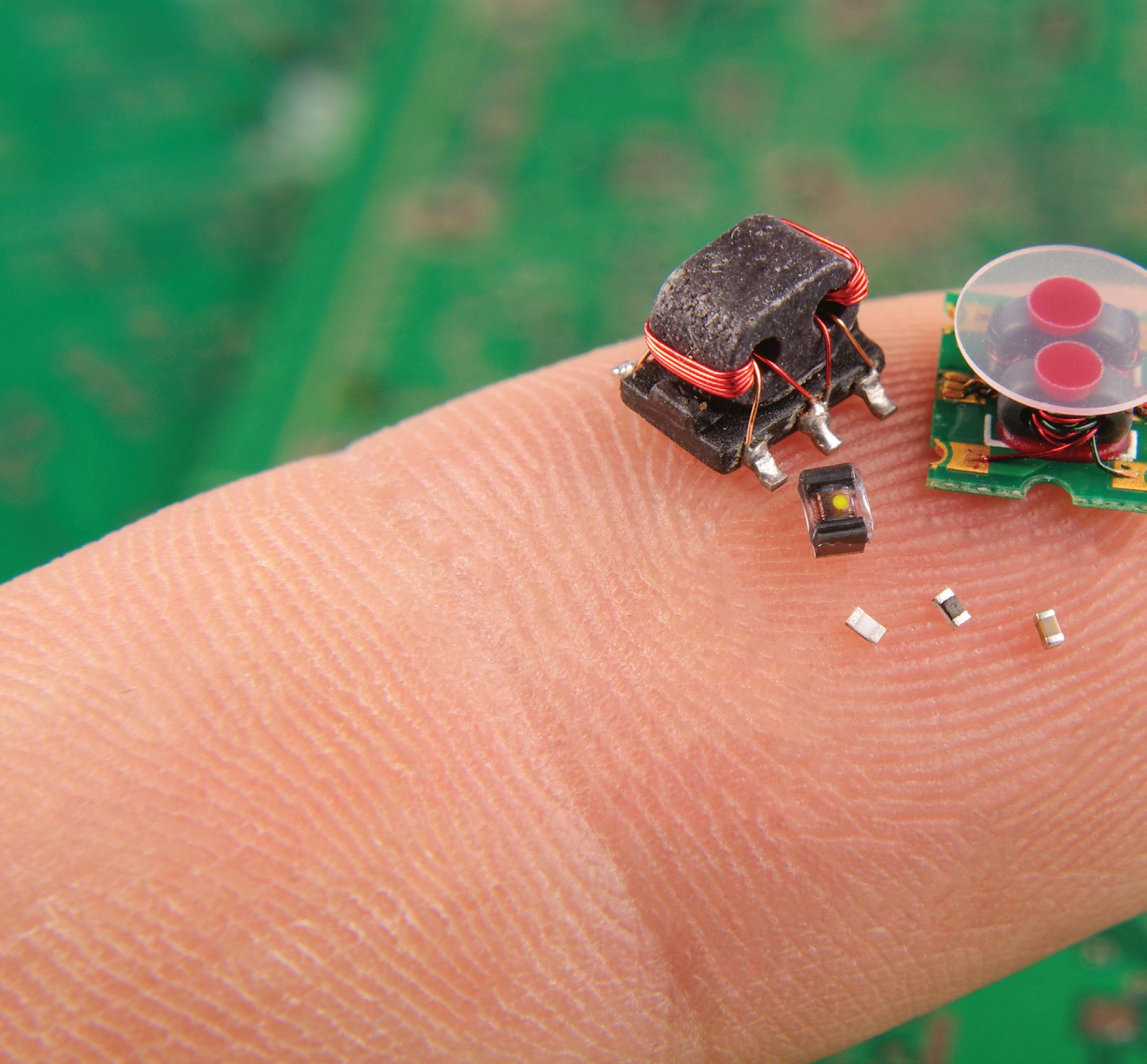
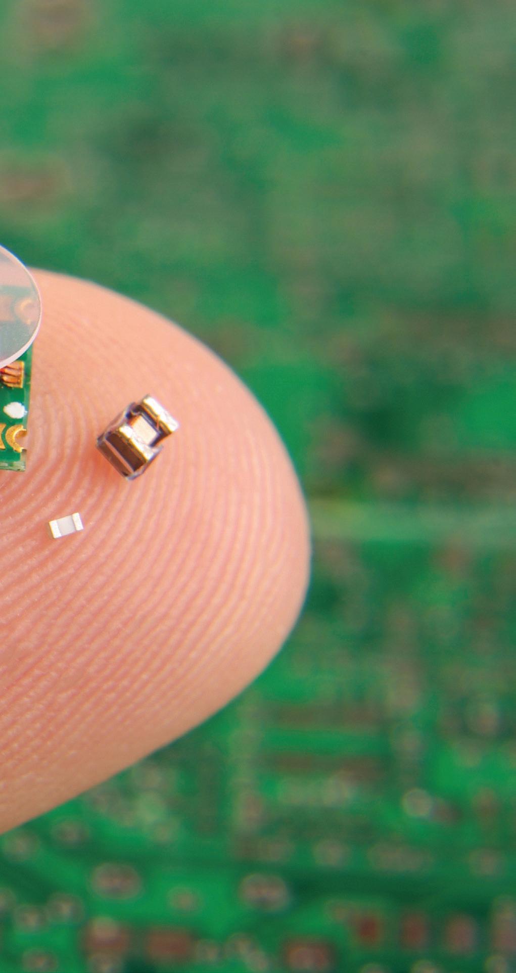
Although at first glance a potentiometer and a rheostat look similar, they serve different functions — one controls voltage, the other current. Additionally, there are thermistors, photoresistors and other variable components that react to light, temperature or pressure.
How do variable resistors work?
Variable resistors allow adjustment of voltage, current or environmental parameters by changing resistance in the circuit. Variable resistors belong to the group of electromechanical components, which means they combine mechanical elements with an electrical function. Their operation consists of regulating the resistance value in a circuit — smoothly or in steps — depending on the position of the movable element. Exactly how resistance changes depends on the component’s design and the type of material used.
Principle of operation of variable resistors
A key element of every variable resistor is the screw or sliding contact (wiper), which moves along the resistive track. As this
element moves, the length of the active section of the resistive path through which current flows changes. From a physical point of view, this means a change in resistance, according to the relationship:
R = ρ × (L / A)
Where R is resistance, ρ is material resistivity, L is the length of the conductor (resistive track) and A is its cross-sectional area.
In practice, moving the wiper along the resistive track increases or decreases the path length the current must travel. The effect is an increase or decrease in resistance and thus a change in voltage or current in a given part of the circuit, depending on the connection configuration.
According to Ohm’s law (U = I x R), increasing resistance at a constant voltage causes current to decrease, and reducing resistance increases current flow. This principle applies both to simple volume controls and to power supplies, sensors or power controllers.
Basic construction of variable (adjustable) resistors
A typical variable resistor consists of several key elements whose properties affect the durability, precision and application of a given model.
Resistive track — it is the element along which the wiper moves. It can be made from various materials, including:
• carbon — cheap, commonly used, with average durability;
• cermet — ceramic-metal composite, stable and precise;
• resistive wire — usually used in high-power rheostats.
Wiper — a movable contact that slides along the resistive track. It can be driven by:
• knob — in rotary versions (eg, panel potentiometers); adjusting screw — in trimmer versions intended for single calibration;
• linear slider — in sliding potentiometers, eg, used in audio mixers.
Enclosure — Variable resistors come in versions:
• panel — with a shaft protruding through the device housing, allowing user access;
• mounting (on PCB) — used inside electronic circuits, often as trimmers;
• SMD — miniature version for automatic mounting on printed circuit boards.
Each of these variants can be optimised for different uses — from manual user adjustment to precise laboratory calibration.
The principle of operation of all variable resistors is based on the same rule — changing resistance by moving the contact along the resistive track. However, differences concern construction, number of terminals and purpose. This section looks at the basic types of adjustable resistors, starting with the most common — the potentiometer.
Potentiometers
A potentiometer is the most popular type of variable resistor, equipped with three terminals. The two outer terminals are connected to the ends of the resistive track, and the third to the wiper, which allows reading voltage from any point on the path. This configuration enables the use of the potentiometer as a voltage divider, where the output voltage depends on the wiper position.
Depending on construction, potentiometers can be:
rotary — with a classic knob, often mounted on front panels of devices;
• sliding — where the slider moves linearly, facilitating intuitive adjustment (eg, in audio mixers);
• digital — without mechanical drive, controlled by digital signals (eg, I2C), used in microcontroller-based systems.
Potentiometer applications are very broad. They are found in:
• volume, tone and balance control in audio equipment;
• brightness adjustment in lighting circuits;
• signal level changes in analog paths;
• as input elements in user interfaces (eg, MIDI controllers, synthesisers).
Thanks to their simplicity and versatility, potentiometers remain the fundamental regulation tool in consumer and industrial electronics.
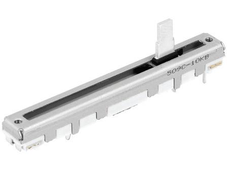
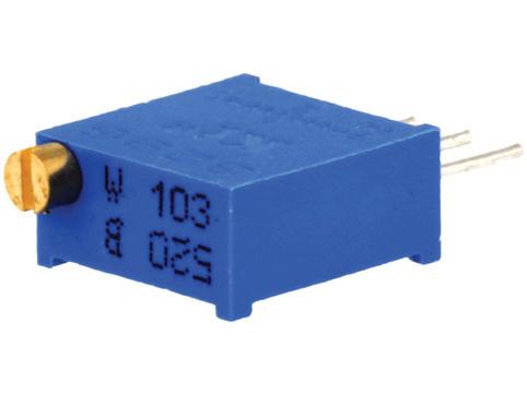
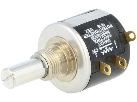
A rheostat is the simplest functional type of variable resistor. It operates using two terminals, one connected to a fixed end of the resistive track, and the other to the wiper. Unlike a potentiometer, it does not act as a voltage divider — its task is to adjust series resistance in the circuit, which directly affects current intensity.
Rheostats are particularly useful for:
• smooth brightness control of traditional light sources (dimming); limiting starting current in electric motors; manual temperature control of heaters and heating elements.
Their simple construction makes them durable and intuitive to operate. However, it should be remembered that they operate by dissipating power as heat, making them energy inefficient. For this reason, many applications now use electronic circuits with higher efficiency, such as PWM control. Alongside potentiometers and rheostats, there is a group of variable resistors intended not for frequent user operation but for precise setting of circuit parameters at start-up, testing or servicing. These are trimmers.
Trimmers are miniature mounting potentiometers designed for direct installation on a printed circuit board. Unlike panel potentiometers, they have no shaft or knob. Their adjustment is made using an adjusting screw, usually with a small screwdriver. This operation method clearly indicates their purpose for technical calibration rather than user adjustment.
Trimmers are most often used for:
• setting reference voltages in power supplies and converters;
• calibrating sensor trigger thresholds; tuning generators, filters and analog paths.
They come in both single-turn versions, allowing quick, coarse adjustment, and multi-turn versions, which enable very precise tuning thanks to a greater number of screw turns. Due to limited mechanical durability and lack of easy access, trimmers are designed for rare adjustment. After correct parameter setting, they usually remain unchanged for the device’s entire service life, ensuring stable and repeatable circuit operation.
Thermistors, photoresistors and others
Besides mechanically operated components, there is a group of variable resistors reacting to environmental changes. These are semi-passive elements that automatically adjust resistance value depending on a specific physical factor.
Thermistors are divided into two basic types:
• NTC (Negative Temperature Coefficient) — resistance decreases with increasing temperature;
• PTC (Positive Temperature Coefficient) — resistance increases with higher temperature.
Thermistors are widely used in temperature sensors, thermal protection and HVAC systems.
Photoresistors (LDRs) — their resistance decreases with increasing light intensity. Used in:
• automatic lighting circuits;
• light meters;
• detectors of changing lighting conditions.
Resistors sensitive to other factors — There are also elements whose resistance changes under:
• pressure force (force sensors, pressure mats);
• humidity (humidistors — used in IoT devices);
• magnetic field (magnetoresistors, used in position encoders).
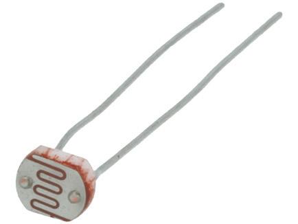
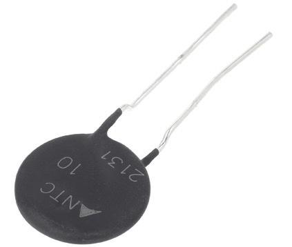
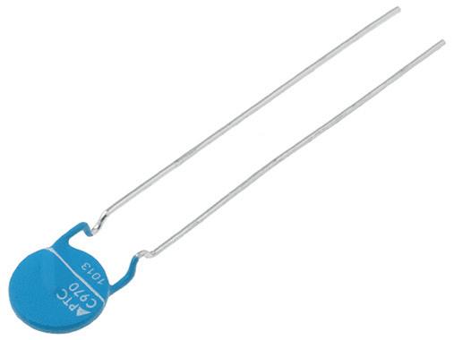
Although not classic components for manual adjustment, their operation is based on the same principle — dynamic resistance change, making them an important part of the variable resistor family.
Practical applications of variable resistors
Though variable resistors may seem simple, their applications span a wide range of fields — from everyday devices to advanced industrial systems and research prototypes. Properly selected potentiometers, rheostats or thermistors allow not only parameter adjustment but also dynamic adaptation to environmental conditions.
Consumer electronics
In everyday devices, variable resistors function as an interface between the user and the electronic circuit. They enable manual adjustment and customisation to individual needs.
• Volume, contrast and brightness control
• Sensor calibration
• Fan and motor control
Automation and industry
In industrial environments and automation systems, precise voltage or current control is crucial for safety, stability and efficiency of machine operation.
• Setting threshold voltage levels
Potentiometers are used in comparator circuits, analog-to-digital converters and voltage protection circuits to define the level at which the system reacts.
• Adjusting machine operating parameters
In devices such as temperature regulators, workshop power supplies, or motor controllers, variable resistors allow precise tuning depending on process requirements
• Applications in HVAC, IoT and automotive
In HVAC systems, potentiometers are used to set thermostat sensitivity or airflow strength, though increasingly replaced by digital control or sensor interfaces. In IoT solutions, adjustable resistors calibrate environmental sensors. In automotive, they regulate dashboard backlighting, seat adjustments, or steering assist resistance.
Education and prototyping
Variable resistors also play a huge role in electronics learning and in designing and testing new solutions.
• Presets (trimpots) in test circuits
On test boards and prototypes, trimmers serve as components enabling one-time, precise adjustment of circuit parameters, such as frequency, reference voltage or sensor range.
• Mounting on breadboards and prototypes
Potentiometers mounted directly on breadboards allow quick testing of different resistance values without soldering or component replacement.
In all these areas, variable resistors serve not only as regulation tools but also as elements providing design flexibility and ease of adaptation to changing user or environment requirements.
Selecting the right variable resistor is critical for proper circuit operation. A poorly chosen component can result in imprecise adjustment, shortened lifespan, or even damage to other parts. To avoid such problems, it’s important to consciously analyse both electrical and mechanical parameters and match the resistor type to the specific application.
Technical parameters
Every variable resistor has a set of electrical characteristics that should be matched to the specific circuit.

Resistance range and tolerance
The resistance range (eg, 1kΩ, 10kΩ, 100kΩ) should meet the circuit’s requirements. Tolerance defines how much actual resistance can deviate from nominal value — typically ±10%, but in precise applications components with 5% or lower tolerance are preferred.
Rated power and temperature characteristic
Insufficient rated power can cause resistor overheating. In applications where higher current flows through the resistor, adequate power margin (eg, 0.5 W instead of 0.25 W) should be ensured. Stability in varying temperature conditions is also important, so checking the temperature coefficient (TCR) is advised.
Type of resistive track (LIN, LOG)
The characteristic relating wiper movement to resistance change should suit the circuit function. Linear type works well in most technical cases; logarithmic is preferred in audio systems or where subjective perception of change matters.
Mechanical aspects
Mechanical parameters affect not only mounting method but also user comfort and device durability.
Mounting type
• Through-hole (THT) — facilitates soldering in prototypes and repairs;
• Surface-mount (SMD) — essential in modern, miniaturised circuits;
• Panel — intended for devices with user interface, eg, with knob or slider.
Durability and environmental resistance
For circuits operating in harsh conditions (eg, dust, moisture, vibrations), components with enhanced resistance should be chosen, eg, sealed potentiometers with IP65 protection or made of durable materials like conductive plastic or cermet.
Application matching
The final choice should depend on the function the variable resistor is to serve in the circuit.
• When to choose potentiometer and when rheostat
If voltage division in a divider is needed — choose a potentiometer. For current control in a circuit — rheostat is better. Remember, a potentiometer can function as a rheostat, but not vice versa.
• Preset or manual adjustment
If the parameter is set only once (eg, during device start-up) — a mounting trimmer suffices. For frequent or end-user adjustment — a panel potentiometer works better.
• Type choice when working with a microcontroller
In digital projects (eg, Arduino, ESP32), consider using digital potentiometers controllable via I2C or SPI. They enable automatic calibration, remote control and are more resistant to mechanical wear.
Despite many advantages and wide application, variable resistors have limitations affecting circuit durability and operation quality that should be considered during design and device use.
Limited mechanical lifespan
Variable resistors, especially mechanical potentiometers and rheostats, are subject to wear. The sliding wiper continuously rubs against the resistive track, eventually degrading contact surfaces. This results in loss of adjustment precision and sometimes complete loss of electrical contact.
Overheating risk
Another significant limitation is exceeding allowable power dissipation. Practically, if too large current passes through the resistor, excess energy converted to heat can cause local overheating. Effects include melting the resistive track, burning contacts, or permanent performance distortion.
Electrical noise and interference
In analog and especially audio applications, one common problem is so-called contact noise. It arises at the wiper-track interface, particularly during adjustment. It manifests as characteristic crackling, disturbances or signal level instability. This phenomenon is more noticeable in older or heavily used components and when low-quality materials are used. High-quality analog transmission devices may require manual correction or parameter drift compensation due to this.
Although not every application is sensitive to these imperfections, knowing them helps better match components to specific operating environments and prevent potential problems.
Variable resistors are versatile components that allow precise adjustment of voltage, current or environmental parameters in diverse applications — from simple audio circuits through automation to advanced IoT systems. Depending on construction, they can be divided into potentiometers, rheostats, trimmers and sensor-type variable resistors such as thermistors or photoresistors. When selecting them, electrical parameters, mounting method and intended use — whether calibration or frequent adjustment — are critical.
It is also important to bear in mind the mechanical and thermal limitations of these components. Modern digital potentiometers are playing an increasingly significant role, successfully replacing classic solutions in microcontroller-controlled systems.
Transfer Multisort Elektronik www.tme.com/au/en
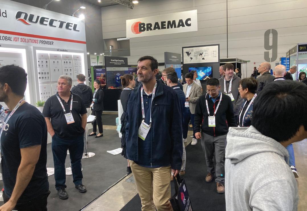
Electronex – The Electronics Design and Assembly Expo, along with the SMCBA Conference, will return to Rosehill Gardens in Sydney from 3–4 June 2026. First held in 2010, Electronex is Australia’s major high-tech exhibition for companies using electronics in design, assembly, manufacture and service, representing over 100 local and international companies with the latest technology and innovations on display.
Electronex features a wide range of electronic components, surface mount and inspection equipment, test and measurement and other ancillary products and services. Trade visitors can also discuss their specific requirements with contract manufacturers that can design and produce turnkey solutions for their products. Noel Gray, Managing Director of show organiser AEE, said “We are delighted with the response, as the Expo is headed for a sellout. Many companies will be launching and demonstrating new products and technology at the event and visitors can discover and discuss how AI is revolutionising the industry.”
The event attracts designers, engineers, managers and other enthusiasts and decision-makers who are involved in designing or manufacturing products that utilise electronics, and is the only
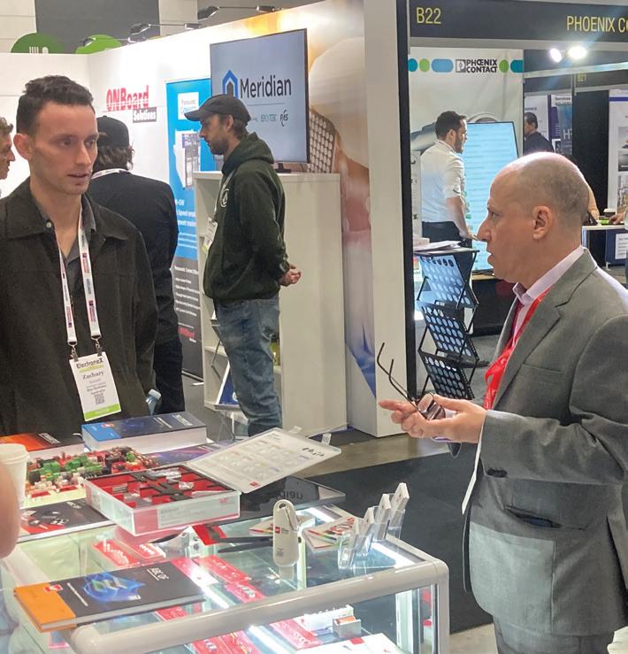
specialised event for the electronics industry in Australia. With many Australian manufacturers focusing on niche products and high-tech applications, the event provides an important focal point for the industry in Australia and is a valuable networking opportunity.
A series of free seminars will also be held on the show floor with visitors able to attend on the day with no pre-booking required. These sessions will provide an overview of some of the hot topics and key issues for the industry. Topics include: Advancing Physical AI, Affordable Yet Versatile Multifunction 12 in 1 Test & Measurement Devices, Power Integrity Measurement Fundamentals, Transforming Test with AI, IoT Beyond Cellular Coverage — 3GPP NTN, Challenges in PCBA Cleaning & Coatings and Design for Manufacturing Masterclass, plus more. Visit the show website for the full program and session times.
Competitions will also be held on the show floor where visitors can test their skills against their peers. The Surface Mount and Circuit Board Association will be staging the highly popular Hand Soldering Competition where contestants can enter on the day in the battle to become Australia’s champion Hand Soldering expert.
A research breakthrough could open the door to more sustainable materials for a range of advanced technologies, from smart coatings, electronics and sensors, to self-healing systems.
Published in the American Chemical Society journal Sustainable Chemistry & Engineering, researchers from Monash University have developed a green, solvent-free method to produce nitrogen-doped graphene nanoplatelets using a bio-derived nitrogen source.
The innovation uses mechanochemistry, which combines materials through grinding rather than chemical solvents, cutting down energy use and eliminating toxic precursors and by-products.
The resulting material shows improved electrical, thermal and mechanical performance. When incorporated into advanced polymer systems, it even demonstrates electrically triggered self-healing, hinting at potential applications in smart, durable materials.
For manufacturers, the process hints at greener production pathways for polymers and composites, reducing chemical waste and energy costs. Materials scientists and R&D teams could explore its use in smart coatings, electronics, sensors and self-healing systems.

While still experimental, the method demonstrates how high-performance materials can be made without harming the environment.
“This method proves that you can make advanced materials without compromising environmental responsibility,” said Chamalki Madhusha, a third-year PhD student in the Faculty of Engineering.


Global supply chains have long been built for efficiency and cost. But in strategic industries, the challenge today is as much political as it is logistical. A new study from the House of Innovation at the Stockholm School of Economics shows how growing rivalry between major powers is pushing firms to rethink where they source materials, place factories and build long-term partnerships.
The study focuses on semiconductors and rare earth elements — two industries that are critical for modern technologies such as electric vehicles, renewable energy and advanced electronics. Both sectors have become focal points in the strategic competition between the United States and China.

Siemens has introduced the Fuse EDA AI Agent system, a new artificial intelligence system that is designed to plan and orchestrate complex semiconductor, 3D IC and printed circuit board (PCB) system workflows, including verification and manufacturing. Supporting NVIDIA Agent Toolkit, advanced Nemotron models and NVIDIA AI infrastructure, the AI system manages workflows across Siemens’ EDA portfolio, delivering automation that accelerates engineering productivity and achieves higher-quality designs.
Amit Gupta, Chief AI Strategy Officer at Siemens EDA, said the AI system moves from in-tool AI capabilities to autonomous, end-to-end workflow orchestration.
“What we see is a clear shift in how companies think about supply chains,” said Constantin Blome, co-author of the study and professor at the Stockholm School of Economics. “Geopolitical considerations are no longer a side issue — they increasingly shape decisions that used to be driven mainly by cost and efficiency, making supply chain design a strategic issue rather than just an operational one.”
Based on interviews with senior managers in high-technology firms operating in the US and China, the research shows a clear shift in how companies respond to political uncertainty. Policies such as export controls, subsidies and localisation requirements have increased uncertainty, making long-term planning more difficult.
Rather than treating new regulations as short-term disruptions, firms increasingly adjust long-term decisions about sourcing, production capacity and supplier relationships. This includes diversifying suppliers, reducing dependence on single countries for critical inputs and, in some cases, relocating or duplicating production to different regions. These changes are often costly, but firms see them as necessary to maintain access to key technologies under uncertain political conditions.
“Firms are not just complying with new regulations,” said Łukasz Bednarski, co-author and postdoc fellow at the Center for Security and Resilience at SSE. “They are re-engineering supply chains to make them more resilient, even if that comes at higher short-term costs.”
The findings highlight a broader shift in global business. Supply chain strategy is no longer just an operational issue — it is tightly linked to national security and industrial policy. For companies, this means integrating geopolitical risk into long-term investment decisions. For policymakers, it underlines how industrial and trade policies directly influence corporate behaviour.
The study also suggests that these changes are likely to persist. As strategic competition continues, companies in critical industries may increasingly operate in parallel supply chain systems, aligned with different geopolitical blocs.
As a result, supply chains in strategic industries are becoming less globally integrated and more politically segmented. The study suggests that companies may increasingly operate parallel supply chain structures aligned with different geopolitical blocs — a shift with long-term consequences for global trade and competition.
This is a modified version of a news item published by the Stockholm School of Economics.
“We are delivering intelligent automation across the complete EDA lifecycle, enabling our customers to reduce design cycles while maintaining high-quality standards. Our open architecture allows customers to integrate their own workflows and models, providing the flexibility required for enterprise-scale AI deployment. This positions the industry to maintain a competitive advantage in an increasingly complex semiconductor and PCB system landscape,” Gupta said.
The Fuse EDA AI Agent features a sophisticated RAG pipeline, a multimodal EDA-specific data lake, specialised parsers for EDA file formats, customisable access controls, support for multiple AI models and an open approach for third-party integrations.
According to Siemens, the AI agent provides automated planning and execution across each stage of chip and PCB development. In the front-end design and verification states, the Fuse Agent supports the automation of architectural exploration, design-planning and register-transfer level (RTL) coding with Siemens’ Catapult software. For digital verification, the Fuse Agent also assists with testbench generation, debugging and more through integration with the Questa One Agentic toolkit.
As designs move to physical implementation, the Fuse Agent assists with place-and-time, timing closure and power optimisation through direct integration with Siemens’ Aprisa software. The AI Agent also accelerates custom design and verification with Siemens’ Solido software.
In 3D IC design, the AI Agent manages power/ground load optimisation and automates the creation of signal path plan clustering in Innovator3D IC software. For PCB development, it aids layout, signal integrity and other analyses in Xpedition and Hyperlynx software. It also supports manufacturing readiness through Tessent for design-for-test processes and integrates with Calibre for optical proximity correction (OPC).










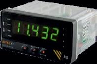
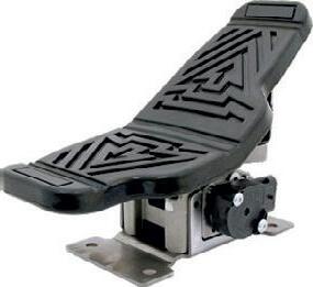

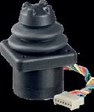
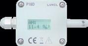



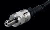
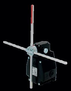
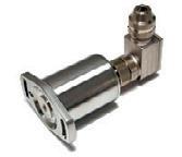
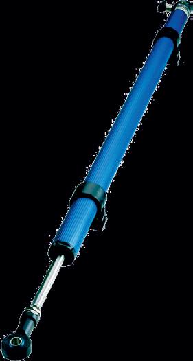
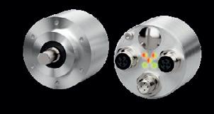
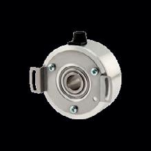
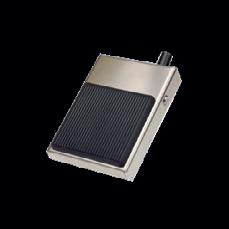
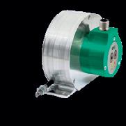


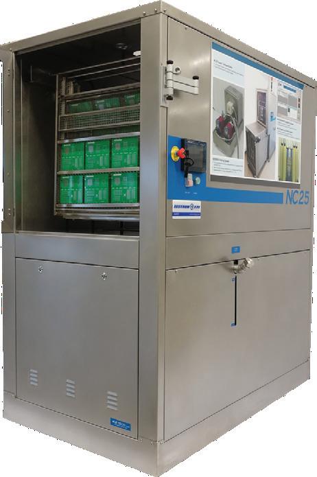
The MB-Tech NC25 is a high-precision parts cleaning system designed for demanding electronics and industrial applications where deposit removal and surface cleanliness are critical. Designed to address a range of contaminants — including flux residues, particulate, oils and process soils — the cleaning system delivers consistent, repeatable cleaning performance with minimal operator intervention.
Built around a robust wash-rinse-dry architecture, the cleaning system utilises controlled spray dynamics and chemical management to achieve thorough cleaning across complex assemblies, fine geometries and mixed-technology boards. Its automatic conveyor and process controls support high throughput without compromising part integrity, making it wellsuited to integration into both batch and continuous production environments.
The system’s modular design allows flexible configuration to match customer process requirements, including ultrasonic enhancement and rinse stage optimisation. With a focus on reproducibility and validated process control, the cleaning system is suitable for manufacturers who require tightly controlled cleanliness standards as part of quality systems or regulatory compliance.
Efficient and adaptable, the MB-Tech NC25 supports manufacturers in achieving both performance and productivity goals in precision cleaning.
ONBOARD SOLUTIONS
www.onboardsolutions.com.au
The DT035CTFT series 3.5-inch colour IPS LCD module features a high-resolution 320 x 480 display that offers sharp detail.

With a bright backlight and wide IPS viewing angle, these displays enable excellent readability and consistent colour performance in both indoor and outdoor environments.
Available with an optional capacitive touch panel, this 3.5″ IPS TFT is a suitable LCD for industrial, consumer and medical devices requiring high-quality visual displays.
IMP ELECTRONICS SOLUTIONS PTY LTD www.imppc.com.au
The Yamaha linear-motor (LM) head is designed for the YRM-series of pick-and-place machines, addressing the accelerating trend towards automated placement of odd-form and specialised components in SMT (Surface Mount Technology) production.
There are a range of factors driving this technology, including the automation of manual processes. Odd-form components (such as large connectors, transformers and sockets) historically required manual assembly, which is slow and errorprone. High-capacity heads like the LM head bring these parts into the automated inline process to improve yield and reduce labour costs.
The need for high-capacity placement solutions is also accelerating across multiple industries, as modern electric vehicles (EVs) require heavy-duty, high-current connectors and power modules that standard SMT heads cannot lift or place. The expansion of generative AI has also increased demand for large, high-pin-count components such as BGAs and FPGAs, which require the precise force control and handling capability of LMclass heads.
Some manufacturers also require ‘all-round’ flexibility to handle both tiny 0201 chips and larger 500 g components on the same line. The LM head’s ability to mount parts up to 90 x 139 mm and 40 mm in height allows for this range.
The LM head addresses these factors with 100 N placementforce management for press-fit parts and vision software recognising up to 20,000 BGA balls. The LM head is available through Hawker Richardson.
HAWKER RICHARDSON www.hawkerrichardson.com.au
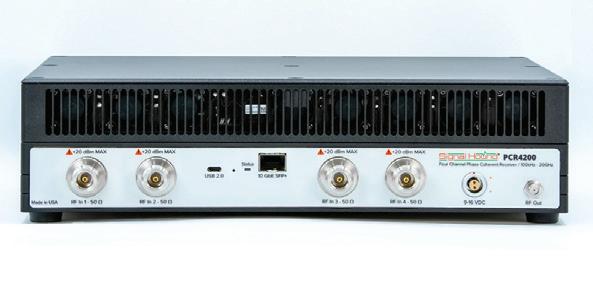
The PCR4200 is a high-performance, 100 kHz to 20 GHz, fourchannel, phase coherent receiver, streaming I/Q data over a VITA 49 interface.
Each channel on the receiver may be configured as a phase coherent channel using the high-performance shared local oscillator (LO), or independently tuned using that channel’s dedicated LO. Additionally, any single channel may be configured to provide swept spectrum data at up to 200 GHz/s. Other features include a builtin 30 MHz to 20 GHz vector signal generator to simplify system alignment and calibration, and an internal GPS to provide precise time, frequency and location.
The receiver is designed to stream 40 MHz bandwidth per channel over 10 GbE SPF+, with calibrated I/Q data. The receiver also features ultra-low phase noise, at –136 dBc/Hz, with 10 kHz offset from 1 GHz centre frequency. Suitable for simultaneous multi-band spectrum monitoring, the receiver has a 110 dB dynamic range and up to 16 phase coherent channels.
Other applications include emitter detection and geolocation, multi-channel transmitter testing, SIGINT/COMINT/ELINT, drone detection and MIMO channel testing.
The PCR4200 also excels at multi-channel, wide-band, simultaneous monitoring applications.
SILVERTONE ELECTRONICS
www.silvertoneelectronics.com
The Glyn D1SE DIN rail power supply is designed to facilitate outputs of 120, 240 and 480 W. The single-phase power supply is designed to reduce energy consumption and optimise the balance between performance and cost-efficiency.
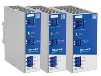
The D1SE series demonstrates a consistent response to evolving system requirements. In addition to conventional operation with AC voltage, the devices can alternatively be operated with DC voltage. Equipped with push-in terminals, the power supplies can be mounted quickly, thereby reducing installation times or even enabling automation. For applications in challenging environments, separate models with coated printed circuit boards are available. The compact design and easy assembly make the D1SE series suitable for a variety of control cabinets, machines and production systems.
GLYN LTD
www.glyn.com.au


THE MODERN WORLD IS INCREASINGLY DEPENDENT ON RELIABLE BATTERY TECHNOLOGY, FROM ELECTRIC VEHICLES (EVs) AND HANDHELD DEVICES TO RENEWABLE ENERGY STORAGE. IMPROVING PERFORMANCE WHILE REDUCING BATTERY WEIGHT AND SIZE IS CONSEQUENTLY A KEY FOCUS ACROSS MULTIPLE INDUSTRIES.
There is a growing consensus that solid-state batteries will deliver the next technological step change.
This relatively new type of battery is arguably lighter, safer and stronger than existing lithium-ion (Li-on) devices, and has a greater energy density.
Growth forecasts indicate a huge appetite for this new battery technology. In 2022, the global solid-state battery market was valued at $126.7 million. Its predicted valuation by 2030 is $1.646 billion. That’s a compound annual growth rate of almost 40% during the forecast period.1 One thing is certain: the solid-state battery market is set for significant growth, regardless of any technical challenges that must be overcome to scale up production.
Part of the attraction of solid-state batteries lies in the shortcomings of existing rechargeable battery types. Although technologies such as Li-ion have advanced rapidly in recent years, they have inherent
limitations that restrict the performance of many electronic devices.
Weight and capacity are two ongoing issues. In the automotive sector, these attributes can limit the range of an electric vehicle. In portable consumer devices, heavy batteries with limited capacity result in a bulkier design and frequent recharging. Safety is another area of concern. The liquid electrolyte that contains the lithium ions is highly volatile and flammable. It represents a potential fire or explosion risk, particularly when exposed to high temperatures or when the battery is overcharged.
The race is on to find alternatives to traditional liquid electrolyte cells that offer higher energy densities and enhanced safety measures. Assuming that technical hurdles can be overcome, solid-state batteries are the odds-on favourite because their underlying chemistry addresses many of the current weight, capacity and safety limitations inherent in traditional battery design.

A typical Li-ion battery cell comprises two solid electrodes (the cathode and the anode), a central separator that acts as a mechanical barrier, and the liquid Li-ion electrolyte. By contrast, a solid-state battery consists of a solid ceramic or polymer substrate that serves as both separator and electrolyte. This arrangement effectively separates the cathode and the anode, which typically consists of pure lithium.
Solid-state batteries can use various types of solid electrolytes, each with unique properties. Ceramic electrolytes, for instance, offer high ionic conductivity and thermal stability, while sulfide electrolytes provide greater flexibility and improved ionic movement. Replacing flammable liquid electrolytes associated with Li-ion batteries with non-flammable solid electrolytes in solid-state batteries reduces risks such as thermal runaway and electrolyte leakage.
The different construction and pure lithium anode that characterise solid-state battery
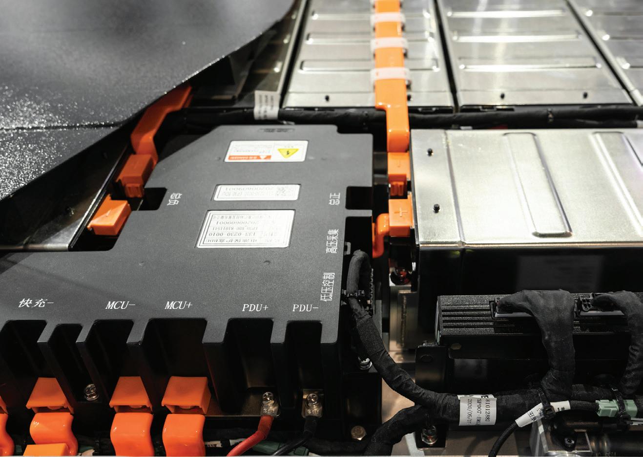
design help to achieve significantly enhanced energy densities. Solid-state batteries can potentially deliver energy densities as high as 11 kWh/kg, although a more realistic value in the short term is around 1 kWh/kg. In addition to surpassing the capabilities of current battery cells, solid-state technology could deliver a weight reduction of up to 30% for the same capacity.2
Superior weight-to-energy performance opens up many potential applications for solid-state batteries. One example is in automotive design, where increasing the battery pack energy density allows vehicle designers to reduce the total pack size, increasing the vehicle’s payload, or helping to boost its range. The advantages for the enduser — including improved energy efficiency, longer travel distances and fewer recharging stops — could be sufficient to convince more commercial vehicle operators and private car owners to switch from internal combustion engine-powered cars to EVs.
Many consumer electronics would also benefit from using solid-state batteries as an energy source. In addition to higher energy density, factors such as increased safety, longer lifespan and improved design flexibility are compelling reasons for incorporating solid-state technology into smartphones, laptops and wearables.
Looking further ahead, solid-state batteries could also speed up the development of smart cities. Digitisation relies on the widespread use of battery-
powered Internet of Things (IoT) nodes, whether the application is manufacturing or urban development. IoT-based networks collect and analyse data to enable activities such as asset tracking, predictive maintenance, energy management and smart city monitoring. In this context, smaller, safer and longer-lasting batteries can improve performance and reduce the costs of IoT infrastructure, potentially accelerating the adoption of smart monitoring networks.
The potential for solid-state batteries is abundantly clear, but the reality is that several technical and manufacturing challenges must be overcome before the technology is commercially viable. These include production complexities, scaling difficulties, material compatibility and longevity.
Broadly speaking, solid electrolytes have lower ionic conductivity than organic electrolytes, which limits the performance of solid-state batteries, particularly at room temperature. Solid-state batteries can also be relatively brittle, making them less durable.
Solid-state battery production requires the fabrication of thin, defect-free layers of solid electrolyte, plus the establishment of a very precise contact with the electrodes. These processes require highly accurate engineering and control. Scaling such processes presents quality and consistency challenges that must be overcome to achieve commercial viability.
Material selection and cost are further obstacles, according to a 2024 article titled Advancements and Challenges in SolidState Battery Technology: An In-Depth Review of Solid Electrolytes and Anode Innovations. The authors highlight the difficulties in finding suitable materials for solid electrolytes with the required high ionic conductivity, mechanical strength and stability. Many promising solid electrolyte materials are costly or complex to synthesise in sufficient quantities, raising questions over the cost-effectiveness of solid-state batteries. Finding compatible electrode materials that can work efficiently with these solid electrolytes adds another layer of complexity.
Progress with solid-state battery commercialisation
Intensive research is being applied to overcome the materials and manufacturing challenges associated with solid-state battery production. In fact, several companies are close to producing commercially viable solid-state battery products, albeit at a relatively small scale.
TDK, for example, has introduced a proprietary material for its CeraCharge solid-state batteries. This next-generation technology offers an energy density of 1000 Wh/L, approximately 100 times greater than the energy density of the company’s early-stage solid-state batteries. According to TDK, this latest technology could replace existing coin cell batteries in wearable devices such as wireless earphones, hearing aids and smartwatches.3
Conclusion: On the brink of solid-state battery adoption
The excitement across multiple sectors surrounding the potential of solid-state batteries is justified. The technology holds enormous potential in EVs, consumer electronics and IoT networks, due to its inherent weight, safety, durability and energy density advantages, which significantly enhance performance. However, widespread adoption is still a little way off, as engineers grapple with the challenges of manufacturing, scalability and consistency. Despite the challenges, continued advancements in nanotechnology, materials science and electrochemistry will likely help to overcome the barriers to adoption, paving the way for full commercialisation.
1. https://www.precedenceresearch.com/solid-statebattery-market
2. https://electronica.de/en/discover/industry-portal/ detail/solid-state-battery-the-holy-grail-in-batteryresearch.html
3. https://www.tdk.com/en/news_center/ press/20240617_01.html
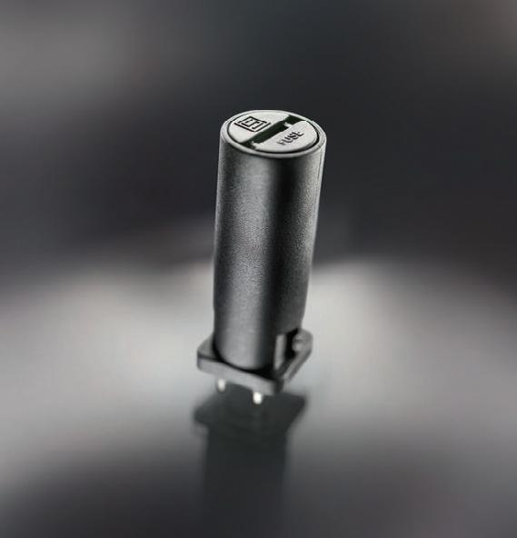
The FPR fuse holder from SCHURTER offers 30% higher power consumption with the same footprint as the well-established FPG4 series. This means more thermal load capacity without taking up additional space on the PCB.
With a power consumption of 3.2 watts at 10 amps at 23°C ambient temperature, the FPR is designed to outperform the previous generation of fuse holders. The housing dimensions remain compact at 12.5 mm, which enables simple 1:1 integration into existing designs. At the same time, the component meets all relevant standards with regard to vibration resistance in accordance with IEC 60068-2-6 and operates in a temperature range of –40 to +85°C. The IP40 degree of protection rounds off the technical profile.
The fuse holder provides developers with a powerful, space-saving and easy-to-install solution that features a high thermal load capacity — all without changing the existing layout. The new fuse holder is fully compatible with the existing FPG4.
The fuse holder is also suitable for applications with high current loads and limited space — for example in industrial automation, mechanical engineering or building automation.
SCHURTER (S) PTE LTD www.schurter.com
At Electronex 2026, Altronics will introduce the T 1348 Rechargeable USB jet blower, a sustainable, high-power solution for cleaning sensitive electronics. Driven by a brushless DC motor reaching up to 130,000 RPM, this fan delivers a concentrated blast of air to remove dust from PCBs, server racks and intricate machinery.
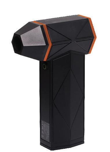
The T 1348 features four adjustable speed settings and a removable magnetic nozzle for precision airflow. With a 2500 mAh internal battery providing up to 2 hours of operation, it is an essential tool with a range of applications. It’s not just a cleaner; it is designed to replace dozens of compressed air cans while offering enhanced, consistent pressure.
ALTRONIC DISTRIBUTORS PTY LTD www.altronics.com.au
STAND C14
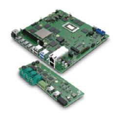
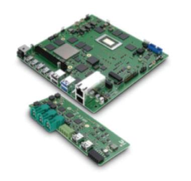
The AMD VPR-7P132 Mini-ITX embedded motherboard features the AMD Versal AI Edge adaptive SoC FPGA devices on a single mini-ITX compute platform. Exhibited at Electronex 2026 by Avnet in collaboration with AMD, this solution enables industrial and automotive developers to leverage multiple compute engines in parallel to process image and sensor data in real time for diverse embedded AI edge applications.
The mini-ITX embedded motherboard is a combination of the AMD Ryzen AI Embedded V4526iX processor (Zen 5 CPU, RDNA 3.5 GPU, 50+ TOPS XDNA2 NPU) with AMD Versal AI Edge Gen2 VE3558 adaptive SoC (ARM CPUs, AI engines).
The Ryzen V4526iX processor supports dual 4K displays, 10GbE, M.2 WIFI, SSD storage and USB interfaces to offload the Versal adaptive SoC of non-time-critical functions. The Versal adaptive SoC is dedicated to real-time pre-processing, AI inference and post-processing low-latency adaptive processing tasks. This solution is available through Avnet, providing easy access to the platform for industrial and automotive developers.
AVNET ASIA PTE LTD www.avnet.com
STAND A3
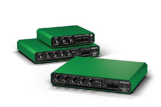
The Analog Discovery Pro 2440 is designed to deliver a range of measurements. Users can choose between four analog channels of either 100 MHz bandwidth at 12-bit resolution (ADP2440) or 200 MHz bandwidth at 8-bit resolution (ADP2450) with seamless integration with WaveForms software. These USB 3.0 oscilloscopes provide the right level of performance where it is needed. Circuit design, embedded systems or a user’s own unique test workflow; it can all be done without distracting from the task at hand.
These USB-based mixed signal oscilloscopes feature an arbitrary waveform generator with 15 MHz bandwidth, a freely allocatable deep buffer memory and 16 digital inputs/outputs to support a variety of communication protocols. The oscilloscopes also come with a bode plot, dedicated FFT, impedance analyser, bus analyser, data logger and more.
DIGILENT INC www.digilent.com





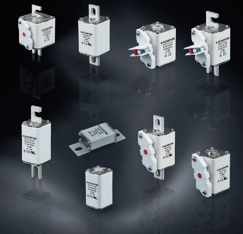
The EKO series of HV fuses is engineered for demanding high-voltage environments, offering protection up to 1000 VDC (and 1250 VAC for selected models) and current ratings from 50–1100 A. With a breaking capacity of up to 50 kA DC, these squarebody fuses are designed to provide safety and reliability.
The EKO series can withstand mechanical vibration, shock, chemical exposure and temperatures from –40 to +125°C. Its ceramic housing and tin-plated copper alloy terminals facilitate durability and stable electrical characteristics even under harsh conditions.
Users can choose from Flush End, DIN-Rail, US Style Bolted Tag or Bolt-on to simplify integration into diverse systems. Optional indicators and microswitches also enable easy status monitoring.
The fuses are suitable for charging infrastructure, energy storage systems (BESS), manual service disconnectors, power conversion devices (UPS, inverters, drives) and heavy industrial equipment.
The EKO series meets IEC, UL and GB/T standards and complies with CE, RoHS and REACH directives, for global acceptance.
SCHURTER (S) PTE LTD www.schurter.com
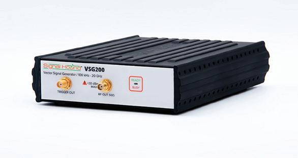
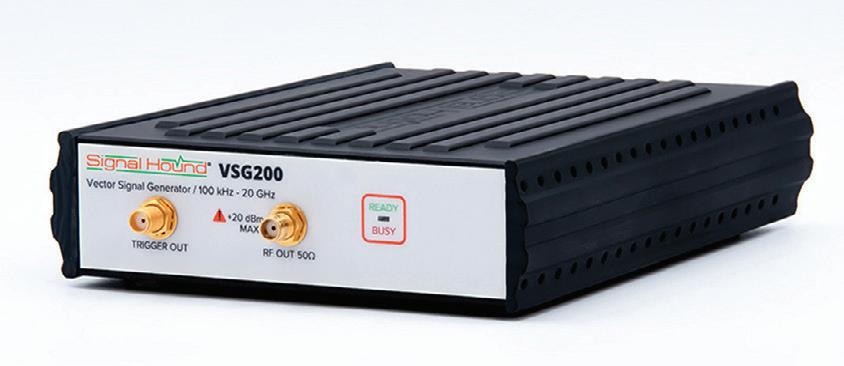
The VSG200 features a low phase noise, agile local oscillator with 200 µs switch time, enabling frequency hopping spread spectrum testing. A dual 14-bit DAC runs at 2x or 3x the I/Q symbol rate using digital oversampling to provide a flat, clean baseband; and a digitally adjustable internal VCTCXO keeps frequency errors to a minimum over temperature, or an external 10 MHz input may be used for zero ppm frequency error. A trigger output is also available to synchronise the VSG200 with other test equipment.
There are a range of modulation types available, including LTE, 802.11a/n/ac/ax, Bluetooth LE, Custom OFDM, 16/64/256/1024-QAM, 2/4/8/16-PSK, 2/4/8/16-FSK, ASK, GMSK, AWGN channels, ramp/chirp, stepped sweep, multi-tone, pulse, FM, AM, CW and arbitrary/custom.
The vector signal generation also supports digital modulation impairments, including channel effects, noise, timing and frequency offsets, amplitude variations and I/Q imbalance.
Users can also utilise the API to continuously stream custom I/Q data to the VSG200 at arbitrary sample rates up to 51.2 Msps. The external trigger output can be used to synchronise multiple instruments for complex measurement setups. Users can also take advantage of the 10 MHz timebase input to ensure frequency coordination between all lab equipment.
SILVERTONE ELECTRONICS
www.silvertoneelectronics.com
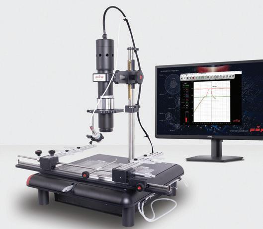
Designed for increasingly complex PCBs, the PDR focused infrared (IR) systems are designed to deliver precise, repeatable rework without thermal shock or unnecessary stress to surrounding components.
The infrared rework system’s focused infrared heating targets only the component being reworked, for controlled, stress-free removal and replacement of BGAs, QFNs, CSPs, LEDs and lead-free devices.
The system’s PC-based, closed-loop thermal management also allows users to control both component and board temperatures, delivering repeatable results and protecting sensitive assemblies.
The rework system features tool-free, gas-free operation with instant thermal response, thereby simplifying setup and creating a cleaner, more efficient rework environment.
From entry-level systems such as the IR-E1 to advanced semi-automated platforms, the rework system’s modular design allows systems to scale as rework complexity and production demands increase.
Exclusively represented in Australia and New Zealand by Hawker Richardson, PDR brings leading rework capability to local electronics manufacturers and repair specialists.
HAWKER RICHARDSON www.hawkerrichardson.com.au
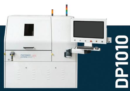
Photonics laser depanelling systems deliver high-precision, non-contact separation of printed circuit boards, enabling manufacturers to achieve clean, burr-free edges without mechanical stress. As board complexity increases with fine pitch, high-density components and complex geometries, traditional mechanical depanelling methods can risk board damage, delamination or component stress. Photonics’ laser-based approach addresses these challenges with a controlled, high-energy beam that cuts the substrate according to programmed patterns.
The system utilises advanced laser optics and motion control to produce consistent, repeatable results across a range of materials, from standard FR-4 to high-performance laminates and flexible substrates. Non-mechanical depanelling eliminates tool wear, reduces particle generation and minimises post-process cleaning, delivering improved throughput and quality for high-mix production environments.
With integrated vision systems and programmable cut paths, Photonics laser depanelling solutions support rapid changeovers and complex board designs. The modular architecture enables seamless integration into SMT and box-build lines, making it well-suited for electronics manufacturers seeking higher yields, greater flexibility and reduced rework.
ONBOARD SOLUTIONS www.onboardsolutions.com.au
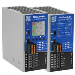
This uninterruptible power supply for DIN rail applications offers safety in the event of a power loss, with a wide input and output voltage range of 10–60 VDC IN and 10–58 VDC OUT. The power supplies also feature decoupled load and battery voltages thanks to an integrated DC/DC converter.
The power supplies offer continuous battery protection due to their NTC sensor, SoC monitoring and Ri measuring. The power supplies also enable system monitoring and control via Modbus/RTU with comprehensive settings, measuring and status parameters.
Thanks to its comprehensive features, the DUSH uninterruptible DC power supplies can be deployed in a range of applications such as industry automation, plant engineering, building control systems, test and measuring technology and information and communication technology.
GLYN LTD www.glyn.com.au
SCHURTER has launched the Pyrofuse-APO Series, a fuse technology that is designed to operate actively and enhance safety. In the event of a short circuit or accident, the control unit sends a trigger signal to an integrated micro gas generator. Within milliseconds, the generator produces high pressure that drives a piston to mechanically sever the solid copper busbar. The resulting arc is safely suppressed in a dedicated extinguishing chamber. The outcome is a complete galvanic isolation in less than two milliseconds — with measured values as fast as 0.9 ms.
The APO Series is rated for operating voltages up to 1000 V and continuous currents up to 400 A. With an ultra-low internal resistance in the range of only a few dozen microohms (µΩ), power losses and temperature rise remain minimal. Its high breaking capacity facilitates safe interruption even under extreme short-circuit conditions, while the fully encapsulated design prevents the release of gases or particles.
SCHURTER (S) PTE LTD www.schurter.com
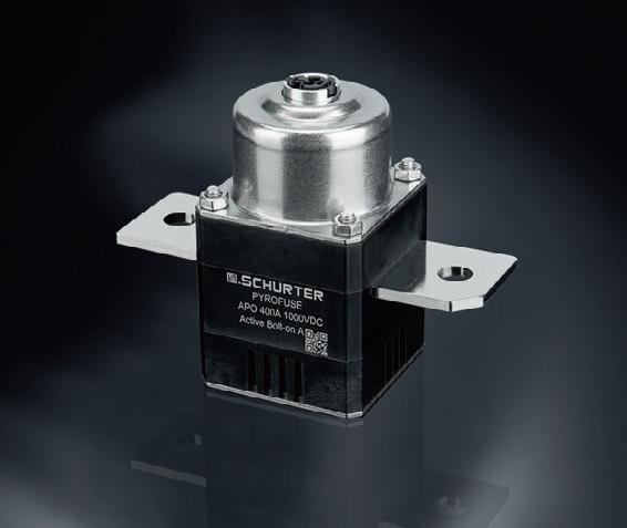
This combination of speed, robustness and efficiency is designed to enable maximum system safety. At the same time, the compact design allows for integration into existing architectures and relieves downstream components such as contactors.
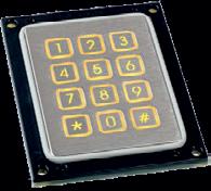
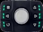
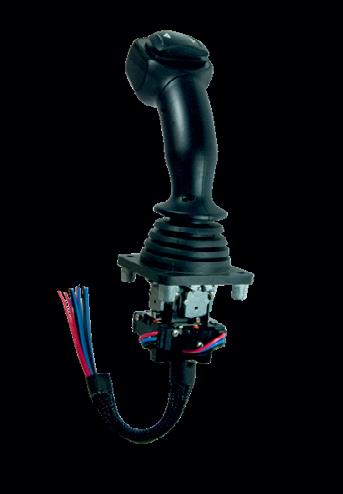
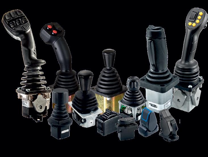
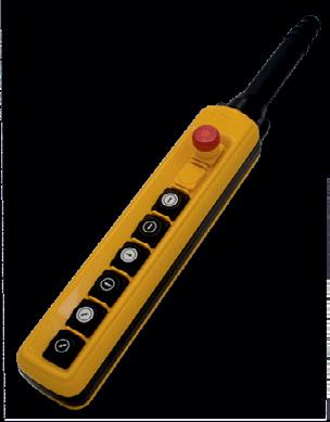
The APEM PKI Series of keypads is a sophisticated solution for complex industrial control. Unlike passive input devices, the PKI Series integrates CANbus technology, transforming a standard keypad into an intelligent node within a networked system.
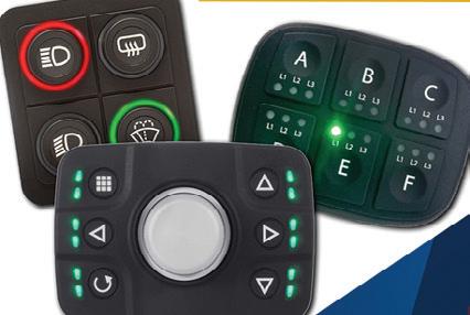
The core strength of the PKI Series lies in its integrated electronics. By utilising the J1939 or CANopen protocols, these keypads reduce wiring complexity, requiring only a four-wire connection to manage multiple functions. This streamlined architecture simplifies installation and enhances system diagnostics.
Designed for rugged environments — from agricultural machinery to heavy construction equipment — the PKI Series features high-intensity RGB LED backlighting for visibility in lowlight conditions, with programmable status indicators for realtime feedback. The keypads are also engineered with silicone keys that provide distinct tactile feedback, even when operated with heavy gloves.
Rated at IP67 and IP69K, the keypads are designed to be resistant to high-pressure washdowns, dust and salt spray.
The PKI Series of keypads merges digital communication with physical durability, enabling critical commands to be executed in a range of harsh conditions.
CONTROL DEVICES AUSTRALIA www.controldevices.com.au STAND C14 STAND B10
STAND D1
The X 4306A HD digital microscope is designed for precision electronics work, biological study and quality control. The unit features a 7-inch HD LCD display (1024 x 600 pixels) that provides a clear view of a range of components.
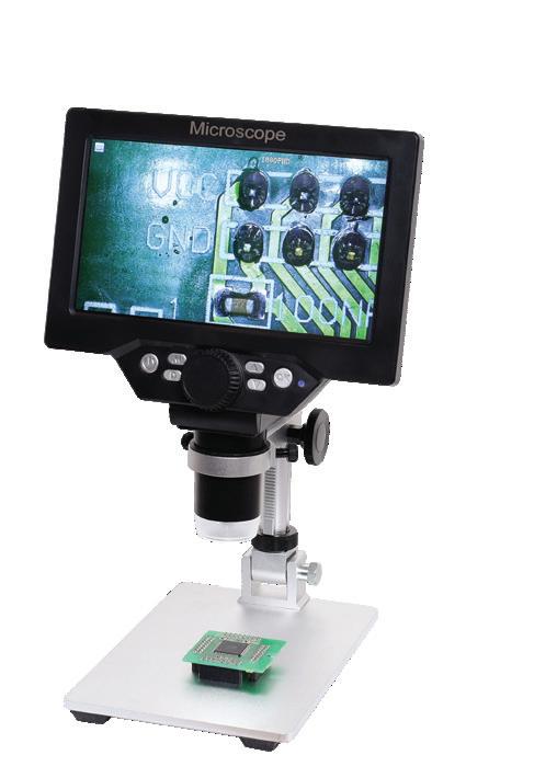
Equipped with a high-performance 12MP camera, the digital microscope offers magnification levels up to 1200x, making it suitable for identifying hairline fractures in solder joints or inspecting intricate PCB traces. The unit features an adjustable metal stand that can tilt up to 45°, allowing for ergonomic viewing and better access for soldering tools under the lens. With onboard microSD recording for photos and video, plus USB connectivity for PC-based analysis, the X 4306A is a versatile tool for any modern lab or workshop.
ALTRONIC DISTRIBUTORS PTY LTD www.altronics.com.au

Spectrum Analysers, Electronic Countersurveillance Systems, Software-Defined Radio and general Test & Measurement.
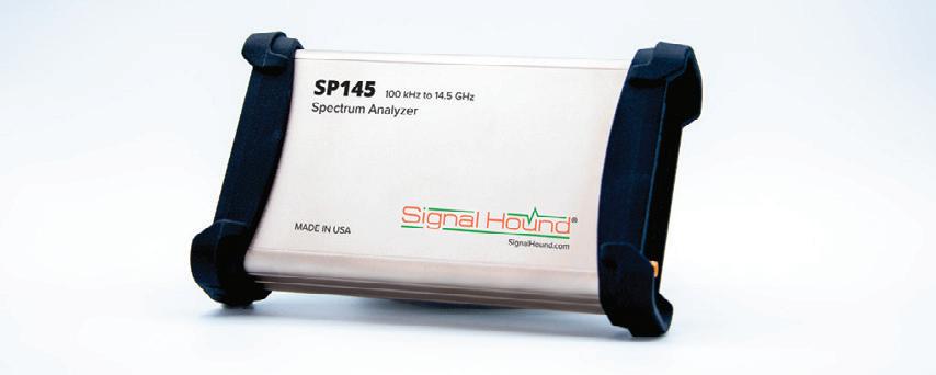
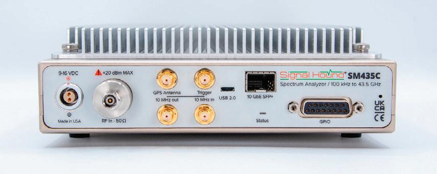
Models for 1Hz – 43GHz, USB and SFP+ models, TeraHertz sampling speeds, 20GHz 4-Channel Phase-Coherent Receiver!
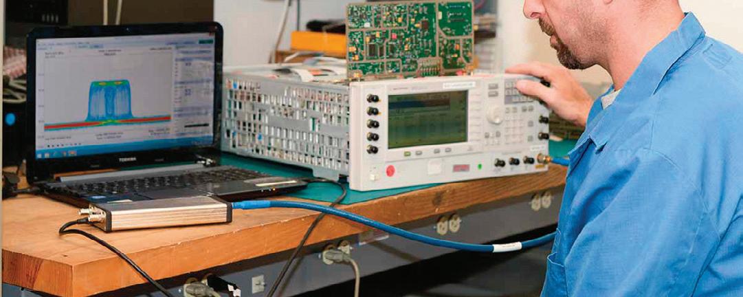
• Full function spectrum analyser on your PC or laptop
• Windows and Linux software supplied
• Full API support for custom applications

Tracking generators to 12.4GHz Vector Signal Generators for arbitrary waveform generation to 20GHz
• 5G/LTE testing
• Spectrum monitoring
• Interference testing
• Workshop, lab and hobbyist applications
• Government and defence users
1/21 Nagle Street Wagga Wagga NSW 2650 Phone (02) 6931 8252 contact@silvertone.com.au

Neil Martin, UNSW

RESEARCHERS AT UNSW HAVE DISCOVERED A NEW WAY TO MAKE GRAPHENE, A REMARKABLE ‘WONDER MATERIAL’, USING DISCARDED PEANUT SHELLS.
The development opens the door to cheaper, more sustainable electronics and energy storage devices, and could help transform agricultural waste into valuable products inside phones and computers that are used every day by billions of people around the world.
“Graphene is famous for being one of the thinnest, strongest and most conductive materials known to science,” said Professor Guan Yeoh, who led the team.
“It is made up of a single layer of carbon atoms arranged in a hexagonal lattice, but is hundreds of times stronger than steel, conducts electricity and heat better than copper and is almost completely transparent.”
Those characteristics make graphene extremely useful in a range of technologies, from batteries and solar panels to touch screens, flexible electronics and super-fast transistors.
However, graphene is expensive and difficult to produce in large quantities — requiring chemicals and energyintensive methods — which is why finding sustainable and affordable alternatives is so useful.
Now, a UNSW team led by Yeoh has developed a process to create graphene from something people usually throw away — peanut shells.
Their research has been published in the Chemical Engineering Journal Advances.
“There are about 55 million tonnes of peanut crops produced globally every year, yet most of the waste from the shell is either discarded or recycled into low-value applications that don’t maximise their full potential,” Yeoh said.
“What we have shown in this work is that basic peanut shells can be turned into high-quality graphene, using much lower energy than is currently required and therefore at a lower cost. We also do not need to use any chemicals, so there is an added environmental benefit.
“Graphene is useful for making stronger, lighter and more conductive materials for applications in electronics, energy storage, medical devices and even flexible technologies like sensors, solar cells and wearable tech.
“The demand for many of those things is increasing rapidly, so it’s exciting to find a way of producing more graphene in a costeffective way — and by using material that would otherwise be waste,” Yeoh said.
is the key
The research team’s first breakthrough was to recognise that peanut shells are packed with lignin, a naturally occurring polymer in plants which contains lots of carbon.
This gave them the idea to grind up the shells and use a series of heat treatments to unlock their potential for graphene production.
The first step involves the shells being heated to around 500°C for five minutes to remove impurities and convert the shells into a carbon-rich char material.
The second step subjects the char to what is known as flash joule heating, in which a flash of electricity rapidly raises the temperature of the material to around 3000°C for just a few milliseconds.
This enormous heat energy instantaneously rearranges the carbon atoms into single layers of graphene.
Current graphene production methods traditionally include carbon black at this stage, an industrial chemical which is predominantly made from fossil fuels like oil and natural gas.
But the UNSW team’s method uses only the peanut-shell derived char itself, thus being more environmentally friendly as well as simplifying the process.
Overall, the new process can be completed in around 10 minutes, offering the benefit of needing substantially lower energy usage than commercial methods in use today.
In fact, their calculations indicate that a kilogram of graphene can be produced using their method at a cost of just US$1.30 in energy.
“What we identified in the experiments was that the most important aspect in terms of producing high-quality graphene was the pre-treatment or precursor engineering done to the peanut shells before the flash joule heating,” Yeoh said.
“That process is vital to remove the impurities and give us the best carbon-rich material to help ensure there are minimal defects in the final graphene and that it is indeed just a single layer of atoms.
“That’s what you want and need to ensure that it has the best properties in terms of conducting electricity and heat.”
Although the amount of graphene that has been produced using the new process is currently small, the researchers are hopeful that with further development the process could be commercialised within three to four years.
And Yeoh said that a range of other organic waste could potentially be used to produce similar results.
“We’ve used peanuts as a test case, but the key ingredient to this process is the lignin which is present in many different plants. We are planning to also carry out experiments with other materials, such as coffee grounds, or banana peels, or anything else that can give us that good char to then turn into graphene.
“Considering how much organic material like that is available, our work demonstrates a good balance between the energy efficiency, the quality of graphene we end up with and the economic viability of the whole process.
“What we have done is really highlighted its potential for use in large-scale biomass-to-graphene manufacturing,” Yeoh said.
This is a modified version of a news item published by UNSW Sydney.
Advantech is set to launch the ARK 3535, the first AMDpowered model in its ARK 3000 series, scheduled for release in March 2026. Designed for edge AI applications in robotics, IoT gateways and machine vision, the controller combines compact design, versatile I/O options and powerful AI computing to meet demanding industrial needs.
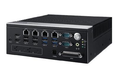
Powered by AMD Ryzen Embedded 8000 Series processors, the controller delivers up to 38 TOPS of AI performance (16 TOPS via the onboard NPU). It supports optional PEG (PCIe x8) expansion and also features USB Type C support, including USB4, DP 1.4a alt mode, and 5 V, 3 A power delivery, enabling high-speed peripheral connectivity at the edge.
The platform offers robust connectivity with four LAN ports (3x 2.5GbE, 1x 1GbE), four USB 3.2 ports and M.2 PCIe expansions, alongside EdgeBMC support for remote management. For users requiring scalable AI performance, the optional AMO 3511 kit provides a PCIe x16 slot (PCIe x8 signal) compatible with Intel Arc and NVIDIA Quadro GPUs, allowing developers to leverage NVIDIA CUDA and Intel OpenVINO toolkits for AI applications.
Compact yet capable, the controller measures 215 x 200 x 75 mm (<2U), making it suitable for space-constrained deployments. Advantech has prepared 20 units per SKU for early production, with full-scale mass production expected by the end of Q1.
The ARK 3535 is a flexible, high-performance solution for developers and integrators seeking manageable and scalable AI computing at the edge. Project inquiries and early access requests are welcomed.
ADVANTECH AUSTRALIA PTY LTD www.advantech.net.au

Challenge: Turning raw machine data into real operational value
Acompany of innovators who tackle problems head-on, Convergix Automation Solutions took action on an issue facing both its OEM and SI customers. The Convergix team noticed that many manufacturers had access to machine data, but not machine data that they could actually use to make decisions. Many of the original equipment manufacturers (OEMs) and systems integrators (SIs) that Convergix serves attempted to monetise dashboards too early, offering visuals without delivering real analytical insight to their own customers.

This left those customers without the clean, contextualised data required to understand performance trends, identify early warning signs of anomalies or degradation, or uncover new value streams.
At the same time, traditional approaches to predictive maintenance focused on detecting machine faults as they were about to occur. This was far too late in the process to take meaningful action. Without consistency in data collection across machines and facilities, both OEM and SI customers struggled to make their operations more predictable, efficient or digitally mature.
Convergix knew that if customers were ever going to extract value from machine data, whether for remote support, further optimisation or AI-driven insights, they needed a foundation of clean, standardised, on-machine data that could be trusted.
Solution:
To address this challenge, Convergix developed Intuition, an on-machine performance monitoring platform included as a standard on every machine it ships. Designed from the ground up to reduce the common pitfalls of early data monetisation, Intuition focuses first on capturing clean, contextualised machine data before any advanced analytics are applied.
The foundation of the solution is FactoryTalk Optix, chosen for its flexibility, OPC UA connectivity and ability to run entirely on-prem. Data is stored in InfluxDB and SQL, visualised through Grafana dashboards, and enriched through time-series tags selected in collaboration with process experts.
By standardising the way its machines collect data, regardless of controller type or customer environment, Convergix created a consistent ‘single layer’ of truth. This trusted source of truth equips OEMs and SIs to provide their customers with remote support, machine-to-machine comparisons, plant-level visibility and AI-ready analysis.
“We didn’t want to predict faults. Predicting a failure is far too late. We went after what leads to the fault: machine performance,” said Jared Comer, Senior Application Specialist, Digital Solutions, Convergix Automation Solutions.
The architecture of Intuition allows customers to operate entirely on-prem with no subscription requirements, while still supporting future layers of predictive maintenance, machine learning and autonomous decision-making.
Result:
With Intuition, Convergix customers now have access to trusted, high-quality data that immediately improves machine visibility and long-term decision-making. The shift from fault prediction to performance-based indicators enables operators to catch issues earlier, reducing unexpected downtime and improving throughput.
What began as an OEM-focused enhancement quickly expanded to full-scale retrofit deployments across major customer facilities. By standardising and unifying data practices across machines, Convergix also created more connections among its OEM and SI businesses, allowing each side to open new opportunities for the other.
Most importantly, customers now have a useful, fully on-prem foundation for future analytics and AI.
“Everybody keeps talking about artificial intelligence and predictive maintenance, but no one’s really been able to crack the nut. We feel like we’re really close, if not already there,” Comer said.
With Intuition, Convergix created not just a performance-monitoring solution, but a scalable foundation for digital transformation. It prepares customers for the next generation of predictive, autonomous and data-driven manufacturing.
Rockwell Automation Australia www.rockwellautomation.com/en-au.html

As mobile machines integrate digital control systems, wireless interfaces and cloud connectivity, cybersecurity becomes a core machine requirement. These technologies increase diagnostic capability and operational efficiency, but also expand the risk of attacks on the machine.
Risks include vulnerable applications, unsecured CAN bus communication, weak password management and malware that can manipulate control logic. Physical tampering or sensor signal interference can also trigger unsafe machine behaviour. Wireless and cloud connectivity add further exposure if encryption, authentication and access control are not properly implemented.
Regulatory pressure is increasing. UN R155 and UN R156 have introduced mandatory cyber security and secure software update management requirements in the EU for on road vehicles since 2021 and are widely used as frameworks for off-highway and mobile machines. The NIS 2 Directive, in force since January 2023, strengthens organisational cybersecurity obligations across critical sectors including transport. From 2027, the EU Machinery Regulation mandates that safety functions must be protected from cyber threats.
Cybersecurity is now both a compliance and safety priority.
Robust cybersecurity begins at the hardware level. Embedding protection directly into the controller architecture creates a secure foundation for the entire machine.
The TTControl TTC 2000 series is an
example of how modern mobile controllers integrate advanced security mechanisms alongside performance and functional safety. These controllers are designed for demanding off-highway environments while incorporating dedicated hardware security features.
The TTC 2000 series integrates a hardware security module (HSM). This enables protected storage and handling of cryptographic keys and certificates directly within secure hardware, making key extraction significantly more difficult. Cryptographic operations such as encryption, decryption and authentication are performed inside the protected environment of the controller.
One of the most important functions is secure boot. Each controller verifies the authenticity and integrity of firmware during start-up, ensuring that only trusted and digitally signed software can be executed. This prevents manipulated or unauthorised code from running on the machine. Additional measures such as secure download processes and authenticated communication interfaces further reduce the risk of manipulation via CAN, Ethernet or other interfaces. By combining secure boot, protected key management and hardware-based cryptography, system integrity is anchored at the lowest level.
This hardware-rooted approach not only reduces the attack surface but also supports compliance with international cyber security standards and regulatory frameworks.
Secure Software with MATCH Hardware protection must be complemented by secure software
architecture. The MATCH development and runtime environment integrates cybersecurity measures across the full lifecycle of the machine.
MATCH enables encrypted communication between controllers, displays and backend systems, protecting data against interception and manipulation. Certificate-based authentication ensures that only authorised devices and services can participate in system communication. Managed key infrastructure supports controlled generation, storage and renewal of cryptographic keys.
Software and firmware updates can be digitally signed and verified before installation, preventing unauthorised or modified code from being deployed. This structured update process aligns with modern regulatory requirements for secure software management.
By combining TTControl’s secure hardware foundation with MATCH’s software implementation, mobile machines can be designed with cybersecurity embedded from the outset. In an increasingly connected world, this integrated approach is essential to safeguard safety functions, maintain system integrity and ensure long-term resilience.
For more information about HYDAC cybersecurity solutions, please visit hydac.com.au.
HYDAC International www.hydac.com.au

Wayne Lewis, UCLA

The lead-acid auto battery of the time, courtesy of Thomas Edison, was expensive and had a range of only about 30 miles (approximately 48 kilometres). Seeking to improve on this, Edison believed the nickel–iron battery was the future, with the promise of a 100-mile range, a long life and a recharge time of seven hours, fast for that era.
Alas, that promise never reached fruition. Early electric car batteries still suffered from serious limitations and advances in the internal combustion engine won the day.
Now, an international research collaboration co-led by UCLA has taken a page from Edison’s book, developing nickel–iron battery technology that may be well-suited for storing energy generated
at solar farms. The prototype was able to recharge in only seconds, instead of hours, and achieved over 12,000 cycles of draining and recharging — the equivalent of more than 30 years of daily recharges.
The technology was built from tiny clusters of metal patterned using proteins that were then bonded to a two-dimensional material, made of sheets only one atom thick. Despite the innovative ingredients, the techniques are deceptively straightforward and inexpensive.
“People often think of modern nanotechnology tools as complicated and high-tech, but our approach is surprisingly simple and straightforward,” said study co-author Maher El-Kady, an assistant researcher in the UCLA College’s chemistry and biochemistry department. “We are just
mixing common ingredients, applying gentle heating steps and using raw materials that are widely available.”
The study was published in the journal Small
The natural world provided some cues for the researchers. Of particular interest was the process by which animals form bones and shellfish form their hard outer casings. Whether skeletons are inside or outside, they’re made by proteins that act as scaffolds for collecting calcium-based compounds.
The researchers sought to mimic this mechanism to generate their tiny clusters of nickel or iron, according to co-corresponding author Ric Kaner, a distinguished professor of chemistry and biochemistry in the UCLA College.
“We were inspired by the way nature deposits these types of materials,” Kaner said. “Laying down minerals in the correct fashion builds bones that are strong, yet flexible enough to not be brittle. How it’s done is almost as important as the material used, and proteins guide how they are placed.”
In the study, the team used proteins that are by-products of beef production. The molecules served as templates for growing clusters of nickel for positive electrodes and iron for negative electrodes. The nooks and crannies in the folded protein structure limited the size of the metal clusters to fewer than 5 nanometres. That’s so small that it would take about 10,000 to 20,000 clusters to match the width of a human hair. The researchers even detected single atoms of iron and nickel in their electrodes.
The proteins were combined with graphene oxide, an ultra-thin 2D material that comes in sheets a single atom thick comprising carbon decorated with oxygen atoms. While the oxygen can create clogs that make the material act more like an insulator, the process that followed changed everything.
The ingredients were superheated in water then baked at high temperature, causing the proteins to char into carbon, stripping away the oxygen in the 2D material and embedding the tiny metal clusters guided by the proteins. The resulting structure was an aerogel, made of almost 99% air by volume.
Part of the technology’s secret sauce is surface area — the more exposed, the more space for the reactions behind battery chemistry to take place.
There was plenty of such room provided by the graphene aerogel’s thinness and

surplus of empty space. And the tininess of the metal nanoclusters takes advantage of a fundamental mathematical principle: as objects get smaller, the size of the exposed outer surface increases far more than volume does.
“As we go from larger particles down to these extremely tiny nanoclusters, the surface area gets dramatically higher,” El-Kady said. “That’s a huge advantage for batteries. When the particles are that tiny, almost every single atom can participate in the reaction. So, charging and discharging happen way faster, you can store more charge, and the whole battery just works more efficiently.”
Despite its advantages in charging speed and durability, this iteration of the technology does not match the storage capabilities of today’s lithium-ion batteries. With range at a premium in the electric car market, the researchers think that this Edison-inspired battery of the future may one day find application in other areas.
For instance, the technology’s fast charging, high output and robust endurance suggest a good fit for storing excess electricity generated at solar farms during the daytime, to power the grid at night. It may also be useful for back-up power at data centres.
“Because this technology could extend the lifetime of batteries to decades upon decades, it might be ideal for storing renewable energy or quickly taking over when power is lost,” ElKady said. “This would remove worries about the changing cost of infrastructure.”
The researchers are exploring the use of their nanocluster fabrication technique with other metals. They’re also looking at possible replacements for bovine proteins, such as natural polymers that are more abundant, and thus less expensive and easier to scale up for future manufacturing.

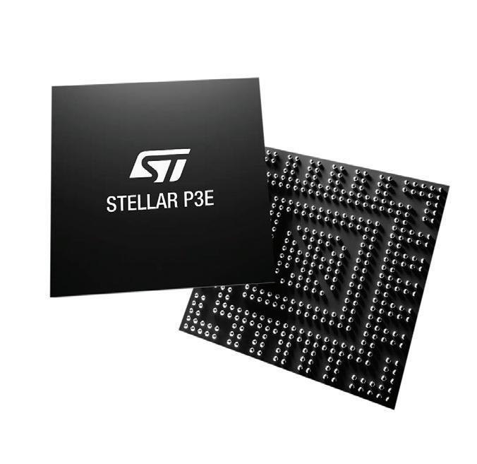
STMicroelectronics has launched the Stellar P3E, an automotive microcontroller (MCU) with built-in AI acceleration for automotive edge intelligence. Designed for future software-defined vehicles, the automotive microcontroller is designed to simplify multi-function integration for X-in-1 Electronic Control Units (ECUs) that reduce system cost, weight and complexity.
The microcontroller features an integrated ST Neural-ART Accelerator for realtime AI efficiency. Powered by this dedicated neural processing unit (NPU) with an advanced data-flow architecture for AI workloads, and combined with its rich sensing capabilities, the microcontroller enables smart sensing that opens the door to new applications such as virtual sensors.
The microcontroller also delivers inference processing at microsecond speeds, achieving up to 30x greater efficiency compared to traditional MCU core processors. This enables always-on, low-power artificial intelligence (AI) that can support real-time functions, including predictive maintenance and smart sensing, delivering benefits across a range of applications. For example, these capabilities can enhance charging speed and efficiency in electric vehicles and enable rapid deployment of new features, whether in the factory or in the field. Original equipment manufacturers (OEMs) can introduce new functions and more intuitive behaviours through different AI models, reducing the need for additional sensors, modules, wiring and integration effort.
The microcontroller’s integrated xMemory, ST’s proprietary non-volatile memory based on phase-change memory (PCM), enables dynamic expansion of software storage to accommodate new features and updates without requiring any hardware redesign.
The start of production of the Stellar P3E is planned in the fourth quarter of 2026. STMICROELECTRONICS PTY LTD www.st.com
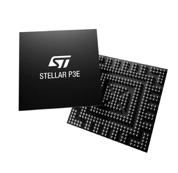
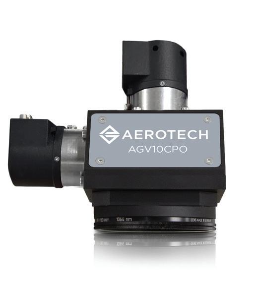
Aerotech Inc., has launched its AGV-CPO CORE Performance 2-Axis Laser Scan Head. Designed to suit a range of laser applications, the laser scan head shares performance capabilities and control hardware with Aerotech’s other 2-axis laser scan heads, thereby allowing users to scale without sacrificing performance or incurring additional control hardware costs.
The laser scan head allows users to control up to 32 servo and galvo axes with Automation1, Aerotech’s unified programming environment that simplifies system integration, enables data visualisation and produces sophisticated, coordinated motion paths. Features include RS-274 compliant G-code programming, motion lookahead and C-transformations.
All Aerotech AGV scanners use digital optical encoders and advanced materials to enable enhanced resolution and dynamics for a range of demanding laser applications.
With Infinite Field of View (IFOV), scanner motion can be integrated with servo stages, expanding the effective working area and eliminating stitching errors or complex part repositioning. This improves accuracy and cycle times.
The laser scan head’s position synchronised output (PSO) also allows for accurate laser firing based on real-time position feedback from the scanner mirror position and any coordinated servo stage positions, for consistent energy delivery during applications like precise cutting, welding and additive manufacturing.
The laser scan head’s integrated motor water cooling and scanner mirror air cooling help to ensure ultra-low thermal drift, minimising process drift over time.
The AGV-CPO is appropriate for a range of laser micromachining applications, including electronics components manufacturing, for display cutting and PCB drilling, as well as semiconductor component manufacturing, for TGV drilling and wafer dicing.
COHERENT SCIENTIFIC PTY LTD www.coherent.com.au
Hammond Electronics has introduced the IP68 1550ZF range, flanged versions of all 18 sizes in the well-established 1550Z rugged, thick-wall, heavy-duty die-cast enclosure family. The full-size flange provides a strong and smooth mounting plate for when the units are secured to a surface. The 18 sizes range from 50 x 45 x 30 mm to 223 x 147 x 83 mm, with the lid thickness ranging from 5 to 33 mm in depth depending on the size. The tongue and groove design and a pre-formed one-piece silicone rubber gasket give IP68 environmental protection, so the enclosures are suitable for installation in environments where dust and water will be present.
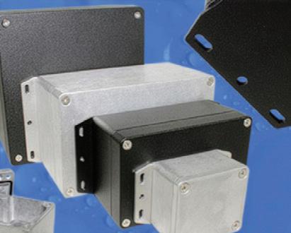
The enclosures are also UL- and cUL-listed and have been independently tested to IP66, IP67 and IP68. They are also rated to NEMA Type 4, 4X, 12 and 13. All sizes except the smallest have an impact rating of IK08, defined in IEC 62262 as the equivalent to the impact of a 1.7 kg mass dropped from 300 mm above the impacted surface.
Depending on the size, the lid is secured to the base with either two, four or six stainless steel Philips machine screws located outside the gasketed area, giving repeated access without degrading the environmental protection. They are available in a natural finish or with a tough polyester black powder finish to both the outside and inside of the enclosure. Clear areas in the painted versions are provided around the grounding points.
HAMMOND ELECTRONICS PTY LTD www.hammfg.com
Teledyne FLIR OEM has launched the Lepton XDS, a compact dual-thermal-and-visible camera module featuring Teledyne FLIR’s patented MSX (Multi-Spectral Dynamic Imaging) technology.
Designed for rapid integration, the International Traffic in Arms Regulations (ITAR) -free Lepton XDS reduces development risk and accelerates time to market for embedded, mobile and industrial applications.
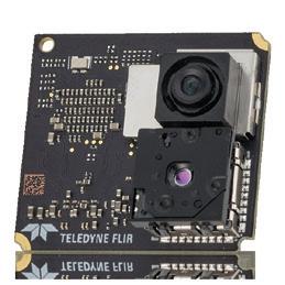
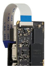
The thermal-visible camera module pairs a 160×120 radiometric Lepton 3.5 micro-thermal camera with a five-megapixel (MP) visible sensor, featuring MSX that enhances thermal imagery in real time by embossing visible-image edges directly onto the thermal scene. This patented software delivers sharper detail, improved context and an enhanced level of actionable thermal intelligence. It is suitable for fire detection and prevention, EV battery monitoring, robotics navigation, unmanned platforms, smart infrastructure and health and safety systems.
The integrated FLIR Prism ISP software enables real-time image enhancement while providing a comprehensive out-of-the-box suite of advanced image-processing features, including thermal-visible fusion, advanced image processing and radiometric JPEG (RJPEG) output. Built-in measurement and visualisation tools include regions of interest (ROI), spot temperature measurements, isotherms and customisable colour palettes. The device is also compatible with the Teledyne FLIR OEM software ecosystem for analysis, post-processing and reporting.
The Lepton XDS is a size, weight and power (SWaP)-optimised module; its USB output makes it well-suited for battery-powered and always-on systems. It is also ITAR-free and classified under 6a993.b.4.b, making it broadly available for commercial applications worldwide.
TELEDYNE FLIR www.flir.com.au
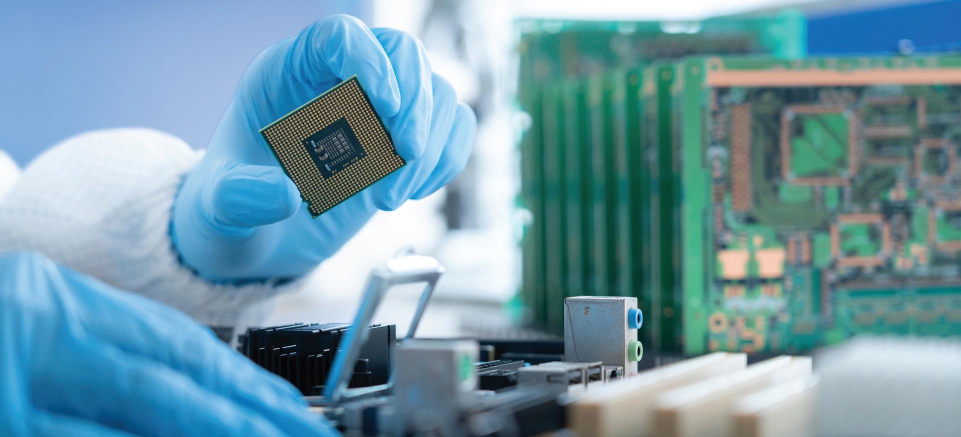
For engineers, timely access to the latest semiconductors and electronic components remains one of the most critical — and often challenging — parts of the design process. Delays in sourcing, limited visibility into emerging technologies, and difficulty obtaining small quantities can all slow development and affect time to market.
This is particularly true when working with next-generation technologies, where early access can significantly influence design decisions and overall product competitiveness. Mouser Electronics addresses these challenges by helping engineers access the newest products through a distribution model designed for speed, availability, and accessibility.
Enabling Early Access to New Technologies through NPI
“One of the biggest challenges engineers face today is not just knowing what’s new — but being able to access those components early enough to design with confidence,” said Daphne Tien, Vice President of APAC Marketing and Business Development at Mouser.
“Every day, new products are introduced by our manufacturer partners. But ensuring these innovations reach engineers beyond early adopters — and are easy to discover and evaluate — is where the real challenge lies.”
According to Tien, Mouser’s New Product Introduction (NPI) strategy focuses on making new products quickly available and easily accessible online, allowing engineers to evaluate and adopt emerging technologies earlier in the design process. This can help accelerate development and support more competitive product design.
Supporting early access on a global scale requires more than broad inventory — it also depends on speed, operational precision, and fulfillment efficiency.
Mouser operates a centralized logistics center in the Dallas–Fort Worth area, which serves as the company’s global operations hub. Originally spanning approximately one million square feet (around 93,000 square meters), the facility was expanded in 2024 with an additional 610,000 square feet (about 57,000 square meters), bringing its total footprint to the equivalent of more than 20 football fields.
The expansion has increased inventory capacity while further strengthening supply chain resilience. Within the facility, automation supports multiple stages of fulfillment, from inbound receiving and storage to order picking and packing.
Mouser currently offers more than 6.8 million components from over 1,200 manufacturers to customers in 226 countries and regions. As an authorized distributor, the company supplies genuine products through manufacturerauthorized channels, providing traceability and quality assurance.
For small-quantity orders, the time from online order confirmation to shipment departure can be as short as 30 to 40 minutes. With no minimum order quantities, engineers can order exactly what they need for prototyping, testing, and iteration.
For customers in Australia, in-stock online orders typically arrive within three to four days, enabling engineers to access the components they need quickly and keep development moving efficiently. This
is complemented by Mouser’s dedicated customer service center in Australia, which provides support in local language and during local business hours.
Looking Ahead: Supporting Future Innovation
As market conditions stabilize, Mouser continues to expand collaboration with OEM and ODM manufacturers while broadening its product portfolio through ongoing NPI efforts.
Tien also noted that continued enhancements to Mouser’s website, mobile apps, and online tools are helping improve how engineers search, compare, and purchase components.
The company is also maintaining a strong focus on sectors such as factory automation and industrial equipment, where demand often centers on a broad range of components in smaller quantities — an area aligned with Mouser’s distribution strengths.
By combining early access to emerging technologies with efficient global fulfillment, Mouser continues to support engineers worldwide. For Australian engineers, this provides not only reliable supply, but also streamlined access to the latest technologies needed to move projects forward efficiently.

The flexible sticker, which attaches to the outside of a drinking cup, collects trace amounts of sweat as a person grips the cup. Within minutes, the system harvests enough power from the sweat to analyse it for vitamin C and wirelessly sends the results to a nearby laptop.
The research findings have been published in Biosensors and Bioelectronics.
“By turning everyday objects like cups or bottles into smart sensors, people can gain real-time insights into their health and wellness without changing a thing about their daily routine,” said study co-senior author Patrick Mercier, a professor in the Department of Electrical and Computer Engineering at the UC San Diego Jacobs School of Engineering. “We’re moving toward a future of ‘unawareables’ — devices that are unobtrusive and essentially invisible so that you are unaware that you’re even using them. You just go about your day and
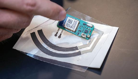
A
ELECTRONIC STICKER THAT CAN MONITOR A PERSON’S VITAMIN C LEVELS USING THE SWEAT FROM THEIR FINGERTIPS — NO BLOOD DRAWS, LAB VISITS OR BATTERIES REQUIRED.
your drinking cup can give you access to all this rich information.”
Malnutrition and micronutrient deficiencies continue to affect millions of people worldwide. While vitamin C plays a key role in immune function, tissue repair and iron absorption, testing for it currently requires blood draws and specialised laboratory equipment. These barriers make frequent monitoring impractical for many people.
The new sticker offers a simple and convenient alternative. Built on a flexible, adhesive polymer sheet, the system integrates screen-printed electronic components. A porous hydrogel pad mounted on the sticker collects sweat from the fingertips. A built-in biofuel cell converts chemicals in the sweat into electricity, which powers a custom printed circuit board and the vitamin C sensor. The circuit board reads signals from the vitamin C sensor and wirelessly transmits the data via Bluetooth low energy.
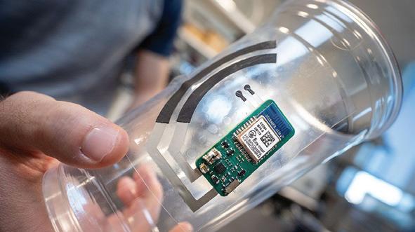
“Most people only get a snapshot of their health once a year at the doctor. But our bodies change much more frequently than that. We want to make access to health data as frequent and effortless as holding your morning coffee cup or orange juice bottle,” Mercier said.
Another special feature of the sticker is that it generates power without requiring physical exertion from the user. Fingertips, despite their small size, are among the body’s most prolific sweat producers — each is packed with over a thousand sweat glands and can produce between 100 to 1000 times more sweat than most other areas on the body. This steady trickle of natural perspiration provides a continuous energy source that allows the sticker to operate even when the user is at rest. Because the system is battery-free, it can be manufactured at low cost — potentially for just a few cents per unit. Its affordability
FAR LEFT The sticker consists of a biofuel cell (black arches) beneath a porous hydrogel pad that collects fingertip sweat, printed circuit board, and vitamin C sensor (small black circles connected to the printed circuit board).
LEFT This battery-free electronic sticker attaches to everyday objects like a drinking cup and monitors vitamin C levels from a person’s fingertip sweat.

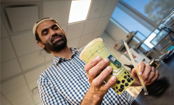
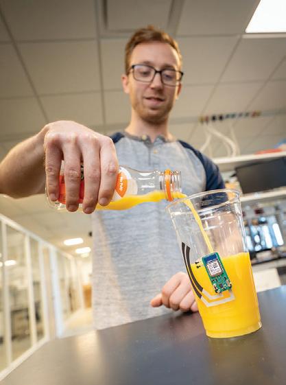
could also make future versions of the system disposable and widely accessible, particularly in low-resource areas.
The work is a collaboration between the labs of Mercier and Joseph Wang, a professor in the Aiiso Yufeng Li Family Department of Chemical and Nano Engineering at the UC San Diego Jacobs School of Engineering.
In tests, the device was stuck onto a disposable drinking cup and accurately
tracked changes in vitamin C levels after participants took a supplement or drank orange juice. The device powered itself for more than two hours using only sweatderived energy.
“This is an elegant extension of our early fingertip sweat-based technology toward effortless, continuous monitoring of personal nutrition and health. By moving sensors from the skin to the surface of
everyday objects like cups or bottles, we are expanding what wearable technology can be,” Wang said.
The team plans to expand the technology to measure additional nutrients and biochemicals. Future versions could send readings directly to smartphones or smartwatches to provide more seamless, real-time tracking of personal health data throughout the day.

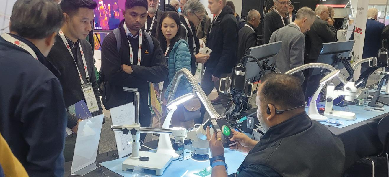
THE SURFACE MOUNT AND CIRCUIT BOARD ASSOCIATION (SMCBA) IS SET TO CONVENE ITS INAUGURAL INDUSTRY SYMPOSIUM, BRINGING TOGETHER A DIVERSE CROSS-SECTION OF PARTICIPANTS FROM ACROSS THE ELECTRONICS SECTOR. DESIGNED TO APPEAL TO BOTH SEASONED PROFESSIONALS AND EMERGING CONTRIBUTORS, THE EVENT WILL ATTRACT ATTENDEES RANGING FROM ENGINEERING SPECIALISTS AND MANUFACTURING EXPERTS TO HOBBYISTS AND PROTOTYPE DEVELOPERS. THIS BREADTH REFLECTS THE INCREASINGLY INTERCONNECTED NATURE OF THE ELECTRONICS ECOSYSTEM, WHERE INNOVATION OFTEN OCCURS AT THE INTERSECTION OF DISCIPLINES AND EXPERIENCE LEVELS.
The symposium aims to serve as a practical forum for engagement rather than a purely promotional showcase. By assembling regional leaders, technology innovators and solution providers alongside the broader electronics community, the event is positioned to facilitate meaningful exchanges of knowledge. Participants will have the opportunity to explore current technical challenges, share operational insights and examine emerging solutions in a collaborative setting. In an industry defined by rapid technological advancement and tight production demands, such knowledgesharing environments are becoming increasingly valuable.
For more than three decades, the SMCBA Conference has played a consistent role in supporting Australia’s electronics manufacturing sector. Historically, it has provided engineers and manufacturers with access to critical technical information as
they navigated rising design complexity, evolving assembly materials and the integration of new manufacturing methodologies. These challenges have only intensified in recent years, driven by factors such as miniaturisation, increased functionality and shifting global supply chains.
The 2026 symposium is being framed against a backdrop of significant industry disruption. Rather than focusing solely on incremental improvements, this year’s agenda will address the broader structural changes required to sustain and advance the sector. A central theme will be the development of a coordinated approach to strengthening sovereign capability in electronics manufacturing — an issue that has gained prominence amid global uncertainty and increasing emphasis on domestic production resilience.
Subject matter experts are expected to

contribute detailed assessments across several key areas, including current manufacturing capability, emerging technologies and evolving customer expectations. The symposium will also consider the role of government policy and strategic investment in shaping the future of the industry. This multi-dimensional approach reflects a recognition that technical progress alone is insufficient; alignment between industry stakeholders and policymakers is also essential.
A distinguishing feature of the symposium will be its focus on outcomes. Rather than concluding with a series of standalone presentations, the event will culminate in the development of an ‘Agenda for Achievement’. This document, drafted collaboratively by participants, is intended to capture the collective priorities and recommendations identified during the conference. It will subsequently form the basis of a formal submission to federal and state governments, providing a structured pathway for industry input into policy development.
This emphasis on actionable results underscores a broader shift within the electronics sector towards greater coordination and long-term planning. As technologies such as advanced packaging, automation and digital manufacturing continue to evolve, the need for cohesive strategies becomes more pronounced. Industry forums that move beyond discussion to tangible outputs are likely to play an increasingly important role in shaping these strategies.
Ultimately, the SMCBA symposium seeks to contribute to the resilience and competitiveness of the Australian electronics industry. By fostering collaboration, encouraging the exchange of technical knowledge and aligning industry perspectives with policy frameworks, the event supports the development of a more robust manufacturing base. In doing so, it also contributes to broader economic objectives, including increased diversification and reduced reliance on external supply chains.
The symposium will be held on Tuesday–Wednesday, 2–3 June at Rydges Resort Parramatta, alongside Electronex, which will run from 3–4 June at Rosehill Gardens, located just across the road. This co-location provides attendees with convenient access to both the conference program and a broader exhibition of industry technologies and services. Together, these events offer a timely opportunity for professionals across the electronics landscape to engage with the challenges and opportunities shaping the sector’s future.
The NAD Electronics CI Modular Series, a compact, scalable platform purpose-built for the custom integration (CI) market is now available through Amber Technology in Australia.
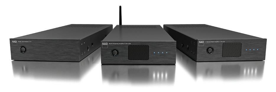
The CI Modular Series features three models that combine high-performance audio, integration and rack efficiency in a compact 1/3U-wide by 1U-high form factor. This will enable integrators to maximise rack space while maintaining flexibility across residential and commercial installations.
The CI Modular Series includes the NAD CI S2 Single Zone Streamer: a versatile streaming solution designed for highquality music playback.
The Series also includes the NAD CI SA2120 BluOS Streaming Amplifier, a powerful streaming amplifier with integrated BluOS for high-resolution, multi-room audio.
The Series features a NAD CI PA4-60 4 Channel Power Amplifier, a robust multichannel power amplifier engineered for efficiency and scalability.
NAD developed the CI Modular Series to support the evolving needs of integrators across new builds and retrofit projects. The ultra-compact design supports dense rack configurations, while BluOS integration provides high-resolution music streaming and multi-zone management.
As part of the BluOS ecosystem, the modular series provides a stable and intuitive interface for high-resolution streaming and multi-room control with integration capabilities for leading thirdparty control systems. Professional AV integrators can design tailored solutions aligned to performance, control and scalability requirements.
In addition to the CI Modular Series, NAD Electronics has updated its CI DSP amplifier range, including enhancements to the CI 8-150 DSP, CI 8-120 DSP and CI 16-60 DSP models. Improvements include a redesigned user interface with a live status dashboard for remote checks, enhanced zone grouping, zone-specific sleep functions, global input flexibility and expanded DSP functionality such as limiters, delay and phase control to support seamless subwoofer integration.
AMBER TECHNOLOGY LIMITED www.ambertech.com.au
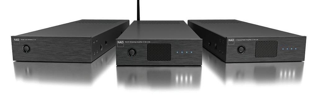

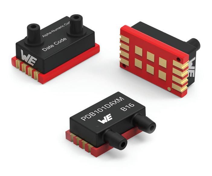
Würth Elektronik has launched the WSEN-PDMS, a differential pressure sensor for a range of operating scenarios. The sensor operates with an accuracy of ±1 mbar and a resolution of 16 bits, supports a broad voltage range from 3.0 up to 5.5 V, and is compatible both with digital I2C and SPI communication interfaces as well as an analog interface. Two different casing versions make the sensor particularly versatile: they are available with vertical straight nozzles for connection with pressure adapters and with horizontal barbed nozzles for tube connection. This flexibility makes both system integration as well as prototype development much easier to accomplish.
The pressure sensor is compatible with a range of microcontrollers and embedded systems. The sensor delivers fully calibrated differential-pressure data as well as optional temperature measurements, and operates in a temperature range from –25 to +85°C. Optionally, the transmitted measurement results can be complemented by additional CRC bits, thus enabling a robust communication.
The pressure sensor is based on the design of the time-tested WSEN-PDUS sensor; like its predecessor, the WSEN-PDMS sensor is suited for a range of applications — from heating, ventilation and air-conditioning technology, filterstatus monitoring, gas-leak detection, and industrial automation, all the way to medical devices such as inhalation equipment.
Like all the sensor products supplied by Würth Elektronik, the WSEN-PDMS series is also available ex stock without any minimum order quantity. It is also possible to develop versions according to the customer’s specifications to meet special application requirements.
WURTH ELECTRONICS AUSTRALIA PTY www.we-online.com
The RECOM RACPRO1-S120 DIN-rail AC/DC power supply delivers 120 W of output in an ultra-slim, space-saving design, making it suitable for compact industrial control cabinets and modern automation systems. With dimensions of 100×28×112 mm, it is designed to help engineers maximise panel density without compromising performance.
The power supply unit features a wide 85–277 VAC input range and offers regulated output voltages of 12, 24 or 48 V, adjustable to suit diverse application needs. High-efficiency operation enables full 120 W power delivery with convection cooling, eliminating the need for forced airflow and reducing system complexity.
Built for demanding industrial environments, the unit includes comprehensive protection features such as overvoltage, overload and short-circuit protection, thereby enabling long-term usage. With international safety approvals and robust thermal performance, the power supply unit is suitable for industrial automation, building control and infrastructure applications across Australia.
RECOM ASIA PTE LTD www.recom-power.com


AT
UNIVERSITY, A RESEARCH LAB’S SIGNATURE KEEPSAKE HELPED PERFECT A METHOD FOR GROWING PATTERNED DIAMOND SURFACES THAT COULD HELP DECREASE OPERATING TEMPERATURES IN ELECTRONICS BY 23°C.
Heat management is one of the major challenges facing today’s high-power technologies, from the gallium nitride transistors used in radar and 5G devices to the processing units powering the data centre infrastructure that supports artificial intelligence. Diamond outshines most other materials when it comes to handling heat, but its hardness makes it difficult to work with. Growing diamond in technology-relevant forms is also challenging.
“In the world of electronics, heat is the enemy,” said Xiang Zhang, assistant research professor of materials science and nanoengineering at Rice and a first author on a study published in Applied Physical Letters. “A reduction of 23°C is significant — it can extend the lifespan of a device and allow it to run faster without overheating.
“Most previous methods for shaping diamond use a ‘top-down’ approach, where they grow a full layer of diamond and then try to carve or etch it down,” Zhang added. “Because diamond is so hard and chemically resistant, that carving process is incredibly difficult, slow and can damage the material.”
The opposite ‘bottom-up’ approach prepares diamond patterns during the growth process itself, building the material literally from the ground up. In this case, Zhang and colleagues in the research
group led by Pulickel Ajayan, a professor of materials science and nanoengineering, used a method known as microwave plasma chemical vapour deposition.
“It entails a reactor that uses microwave energy — like in your kitchen but much more powerful — to turn gas into plasma,” Zhang said. “This plasma breaks down carbonheavy gases mixed with hydrogen, and the carbon atoms rain down and settle onto your substrate.”
The process by which the pulverised cloud of carbon atoms assembles into an ordered layer of diamond crystals on a given substrate is called nucleation.
“Nucleation is like planting seeds,” Zhang said. “Diamond crystals don’t just appear out of nowhere. They need a starting point to latch onto. Nucleation is simply the process of providing that initial foothold that allows the crystals to start growing.”
To control seed placement, the team used two techniques. For small, detailed patterns, they relied on photolithography, a standard method in microelectronics that entails coating substrate wafers with a lightsensitive material, partly exposing them to light to ‘set’ the coating, then washing away any remaining uncured material.
“Think of this as using light to create a precise stencil,” Zhang said. “What is left is
a mold for our diamond seeds. So once the substrate wafers are prepped, we spread a liquid containing nanodiamonds over their surface. These tiny specks act as the starters for the diamond growth.”
For larger wafers, the process needs a different approach. A commercially available film is first laminated onto the wafer, then a laser cuts the desired pattern into the film. The unwanted sections are peeled away, and diamond seeds are applied across the surface. Once the rest of the film is peeled off, all that’s left is a clean, patterned template for diamond growth obtained without harsh chemicals or complex processing.
“This approach allowed us to scale up to a full 2-inch wafer,” Zhang said.
The seeded wafers are then placed in the microwave plasma reactor and showered with carbon atoms that settle onto the seeds, building solid diamond layer by layer.
The new method allows researchers to control not just where diamond grows but how it grows. By adjusting seeding density, they can influence crystal size and structure within a single pattern. As proof of concept, the study tested silicon and gallium nitride substrates, but the method could also be applied to other base layers.

“The main takeaway is that we have found a scalable, effective way to integrate diamond cooling into electronics,” Ajayan said. “This matters because heat is what limits the battery life of your phone and the speed of your computer. By using diamond to cool these devices more efficiently, we can pave the way for faster, more reliable and longer-lasting technology.”
“This work demonstrates wafer-scale, selective diamond growth compatible with heterogeneous integration, enabling high-performance thermal management at device-relevant temperatures and layouts,” Zhao said.
Zhang added that the idea to grow diamond into intricate shapes — including an owl, the university’s mascot — was prompted by wanting to have a special keepsake to give to distinguished guests. He experimented with several different methods over a short period before eventually developing this specific technique for large-scale diamond growth.
“We originally viewed these patterns, such as the diamond owl, more as pieces of scientific art or decoration rather than functional device components,” Zhang said. “Now, we have translated these artistic techniques into a functional application for
the thermal management of electronics. It is incredibly satisfying to be a conduit for this kind of exchange between art making and science.”
Next steps involve perfecting the interface between diamond and other materials to facilitate the development of next-generation high-power semiconductor devices such as high-electron-mobility transistors.
Growing the Rice Owl in diamond: Bottom-up patterning without cutting.
Jorge Vidal, Rice University.
ADLINK has expanded its product portfolio with the ISB-W890 server board, a highperformance, server-class edge AI system. The server board is purpose-built on the Intel Xeon 600 processors, complementing ADLINK’s existing Edge AI platforms by addressing more compute-intensive workloads, enabling real-time vision processing, advanced analytics and large-scale generative AI at the edge.
The ISB-W890 is a CEB form factor server board designed for system integrators who require maximum I/O flexibility and long-term support. The server board features 7x PCIe slots (including 3x PCIe x16 Gen5), enabling multi-GPU scalability for complex inference tasks. It also offers multiple M.2 NVMe and SATA III options to facilitate high-speed data handling.
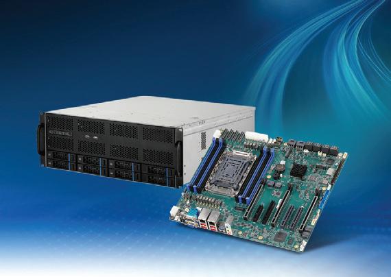
As industries move beyond AI pilots, the demand for server-class performance at the edge is growing rapidly, particularly for real-time visual intelligence and onsite generative AI inference. ADLINK’s Edge AI servers support high-end vision processing and analytics — including VLA workloads — making them suitable for demanding environments like medical imaging, robotics and smart factory AOI, where latency, accuracy and reliability are critical.
ADLINK TECHNOLOGY INC www.adlinktech.com
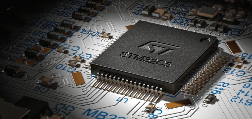
STMicroelectronics has launched a new generation of entry-level microcontrollers (MCUs) to boost the performance of tiny smart devices throughout factories, homes, cities and infrastructures while meeting cost, size and power limitations.
The new STM32C5 series is aimed at consumer and professional devices like smart thermostats, electronic door locks, industrial smart sensors, robotic actuators, wearable electronics and computer peripherals.
The STM32C5 microcontrollers feature an improved design based on ST’s proprietary 40 nm manufacturing process. This gives products more room to include modern features such as improved sensing, smoother control and enhanced user experiences — all while keeping dynamic power consumption low.
The MCUs also integrate built-in protections that help safeguard products against tampering and cyber risks. These security features support safer connected devices, a growing priority across consumer and industrial markets.
The new series of microcontrollers features an upgraded STM32Cube environment, now with size-optimised, production-grade drivers to leverage the many hardware features. The modernised ecosystem also introduces enhanced code generation and development tools as well as extended production-ready software examples.
The microcontrollers are now in production, targeting packages from 3 x 3 mm UFQFPN20 to 20 x 20 mm LQFP144. STM32 Nucleo evaluation boards, and a display extension board from Riverdi with TouchGFX development software for building entry-level graphical user interfaces, are ready to assist development.
STMICROELECTRONICS PTY LTD www.st.com


Leankon has launched a line of Wi-Fi 7, Wi-Fi 6E and Bluetooth integrated antennas. Key products from this line-up include the LK1810101 SMD Bluetooth/Wi-Fi 7 corner mount antenna and the LK1810601 Flex Wi-Fi 6E antenna. Designed for OEMs, IoT innovators and developers of smart tech, the antennas deliver multi-frequency performance and reduce the complexity of wireless systems.
Modern devices require seamless wireless performance across various standards — from ultra-fast Wi-Fi 7 to lowenergy Bluetooth and IoT protocols like Zigbee, Matter and Thread. Leankon’s antennas support these widely used standards in a single component, making it easier to build multi-protocol wireless solutions without sacrificing performance or footprint.
The LK1810101 corner mount antenna is designed to deliver enhanced MIMO performance, omni-directional coverage and compatibility from Wi-Fi 6 to Wi-Fi 7.
The Flex Wi-Fi 6E antenna features an ultra-compact FPC design, making it suitable for small devices that require robust Wi-Fi 7 and Bluetooth connectivity in limited space. Each antenna is designed to offer high efficiencies and optimal radiation patterns tailored for challenging wireless environments.
As smart ecosystems grow, products need to speak multiple wireless languages. A smart speaker may need to handle high-speed data transfers with Wi-Fi 7 while also managing Bluetooth pairing for audio and IoT messaging protocols for connected appliances. Leankon’s antennas support all these signals simultaneously, thereby cutting product weight and improving reliability.
Leankon also provides complimentary evaluation boards and samples so engineers can test designs quickly and effectively. This accelerates time to market and helps development teams enhance antenna performance early in the process.
LEANKON www.leankon.com
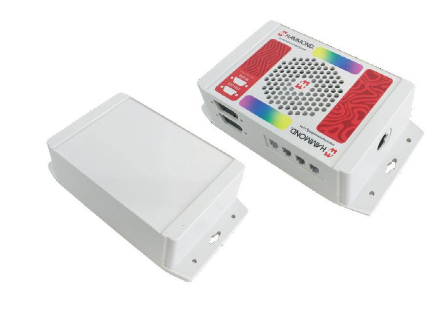

Quectel Wireless Solutions has launched the FGH200M long-range, lowpower Wi-Fi HaLow module. Based on the Morse Micro MM8108 chipset, the module delivers enhanced penetration and broader coverage, over a range of approximately 1 km, while supporting low power consumption and large-scale device connectivity.
The module adopts the IEEE 802.11ah wireless networking protocol, also known as Wi-Fi HaLow, operating in the licence-exempt Sub-1GHz spectrum. Designed to meet the evolving requirements of IoT connectivity, the module delivers extended Sub-1GHz signal coverage, enabling device control at distances of up to 1 km.
With up to 10 times the range of traditional 2.4 GHz Wi-Fi, the module is suitable for both indoor and outdoor IoT deployments. Its long-range, lowpower performance also makes it suitable for applications including home and industrial automation, smart agriculture, smart cities, smart buildings, warehouses, retail environments, campuses and other large-area IoT networks.
Achieving a maximum physical data rate of 43.3 Mbps, the module operates in the 850–950 MHz frequency band with a channel width of 1, 2, 4 or 8 MHz and a maximum output power of 26 dBm. A single Quectel FGH200M access point can, in theory, support up to 8191 IoT devices, making it suitable for massive IoT use cases. The module also supports USB 2.0, SDIO and SPI interfaces to provide maximised integration choices.
With an ultra-compact size of 11.0 x 10.0 x 2.0 mm and weight of just 0.51 g, the module can help to enhance end product size and design cost, thereby meeting the needs of size-sensitive applications. The module is also able to operate in the -40 to +85°C temperature range with security maintained thanks to AES, SHA-256, SHA-384, SHA-512, WPA3 and OWE encryption modes. QUECTEL www.quectel.com







Australian IC design company IQonIC Works, an ASTC Company, is set to launch its 32bit microcontroller platform, the IQMC510x, featuring a sovereign RISC-V CPU core operating at a frequency exceeding 230 MHz. Designed to meet the performance and flexibility requirements of smart sensing, industrial automation, motor and machine control, IoT and AI-driven applications, the platform supports vector and custom instructions, enabling highefficiency execution and flexibility for domainspecific tasks.
Engineered for demanding environments, such as industrial and smart sensing applications, the platform integrates a range of high-performance communication and signal processing capabilities, including 10/100 Mbps Ethernet MAC and six CAN-FD bus controllers for robust, high-throughput industrial networking.
An integrated 12-bit, 500 ksps SAR ADC also enables precise analog signal acquisition in monitoring and control applications. The platform also features flexible serial I/O and rich memory storage.
To accommodate diverse system needs, the MCU platform offers rich peripheral interfaces and flexible memory configurations, including up to 96 programmable GPIOs, plus 4 UARTs, SPI and I2C interfaces. Embedded memory options include 1 MB Flash and up to 512 kB RAM, with 32 kB ROM for first-stage bootloader and flash utilities.
The microcontroller platform also comes with 32 kB instruction TCM (tightly coupled memory) and 32 kB data TCM, both with parity protection, to enable fast code/data access. An integrated QSPI controller also facilitates external flash expansion, supporting storage-heavy applications.
To meet the demands of time-sensitive industrial control, the IQMC510x features a RISC-V CLIC (Core-Local Interrupt Controller) for fast and configurable interrupt handling, multiple timers and a DMA controller for efficient real-time task execution, and PWM control and QEI (quadrature encoding input) with capture/compare functionality for motor control and automation systems.
The platform addresses cybersecurity concerns with AES and SHA-2 crypto accelerators, for strong data protection without compromising system performance.
The IQMC510x platform offers the processing power, flexibility and reliability required for realtime, secure and intelligent embedded systems. IQONIC WORKS iqonicworks.com
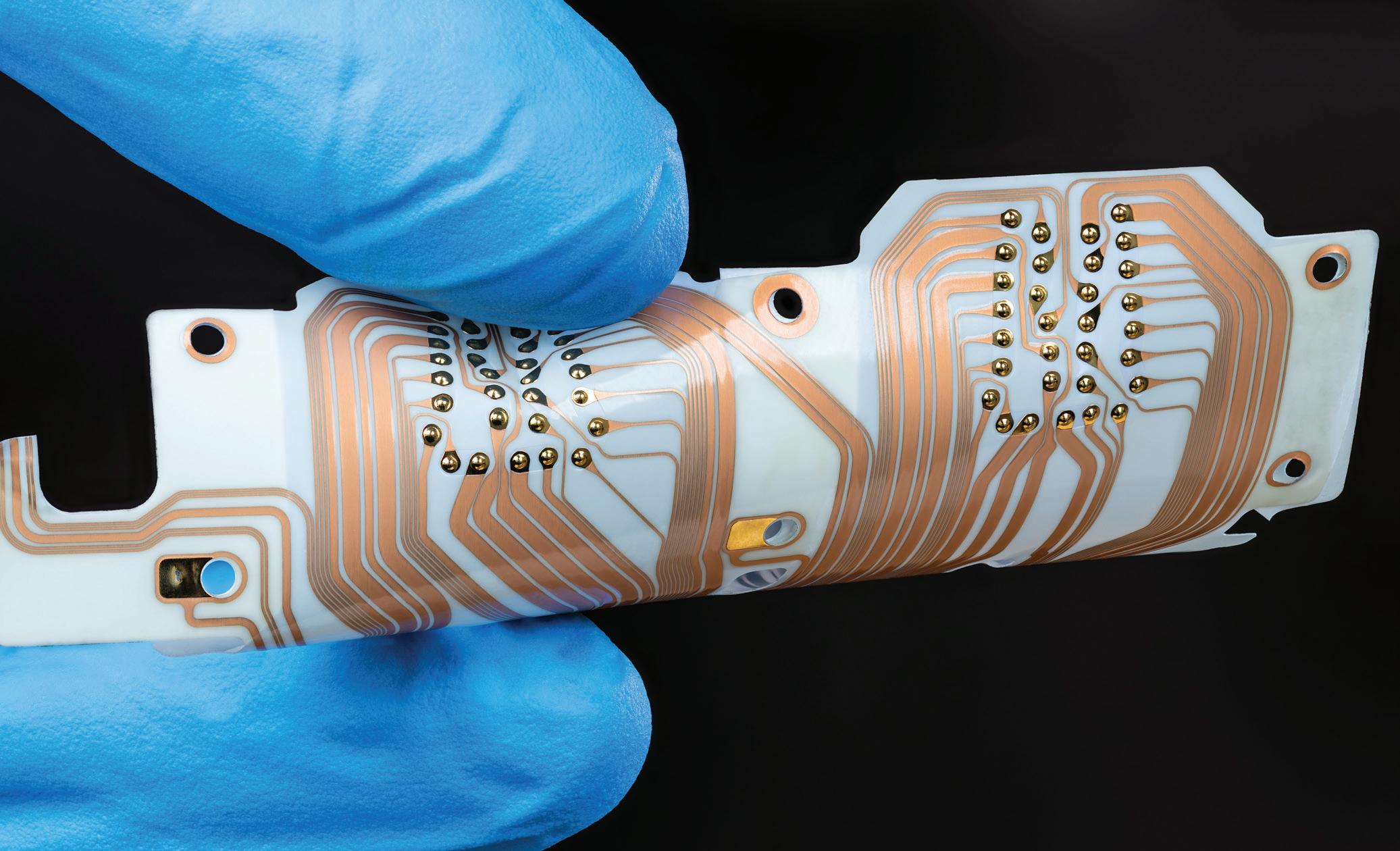
What does ‘flexibility’ actually look like?
FLEXIBLE ELECTRONICS ARE OFTEN SOLD ON A SIMPLE PROMISE: BENDABLE SCREENS, LIGHTWEIGHT SOLAR CELLS OR WEARABLE DEVICES THAT CAN BEND AND FLEX WITHOUT BREAKING. BUT WHAT DOES THAT ‘FLEXIBILITY’ ACTUALLY LOOK LIKE AT THE MOLECULAR SCALE, AND HOW DOES IT AFFECT PERFORMANCE?
Researchers led by the University of Cambridge say they have taken a first step towards answering this question. Using ultra-sensitive atomic force microscopy — which analyses materials by ‘feeling’ them — the researchers were able to measure how stiff flexible semiconductor molecules are when packed together, down to the scale of just a few molecules.
Their findings, reported in the journal Nature Communications, provide the first experimental evidence that the mechanical stiffness of individual molecules contributes to the overall stiffness of a material. In future, the work could help researchers understand whether flexibility places a fundamental limit on the speed and efficiency of future flexible electronic devices.
Unlike silicon, which is rigid and crystalline, organic semiconductors are made from carbon-based molecules that assemble into soft, bendable solids. This flexibility is essential for rollable displays and lightweight devices — but it may come at a cost.
“Silicon electronics are fast partly because silicon is very stiff and orderly, so it’s easy for electrical charges to move around,” said Dr
Deepak Venkateshvaran from Cambridge’s Cavendish Laboratory, who led the research.
“For decades, we’ve built flexible electronics without really understanding what flexibility means at the molecular scale, and whether it might have an impact on how well these materials can conduct electricity.”
To explore that question, Venkateshvaran and his colleagues used atomic force microscopy (AFM), which uses a tiny ‘needle’ — around 10 nanometres wide — to gently press on a surface and measure how much it resists deformation.
“It’s a bit like feeling the ground with a stick,” Venkateshvaran said. “If the ground is firm, it pushes back. If it’s soft, it gives way. We’re doing that, but on the scale of a few nanometres — about the size of a handful of molecules.”
By carefully controlling the force applied to the organic semiconductors by the AFM ‘needle’, the researchers were able to map stiffness across thin films of organic semiconductors with unprecedented resolution.
The team focused on an organic semiconductor called DNTT, which is
widely used in flexible transistors. They compared DNTT with several closely related molecules, each modified with different chemical ‘side chains’ attached to the same rigid molecular core.
These side chains act like molecular padding. Longer, more flexible chains increase the spacing between the rigid cores when the molecules pack together, changing both the structure and the mechanical response of the material.
The AFM measurements showed that materials with longer and more flexible side chains were softer when pressed perpendicular to the surface. Unsubstituted DNTT was the stiffest, while versions with long side chains were significantly softer.
“People have always assumed that adding flexible side chains would soften a material, but no one had ever measured that effect directly at the molecular level,” Venkateshvaran said. “The effect is subtle, and you only see it if you’re extremely careful.”
The researchers then compared their experimental data with computer simulations. The calculations independently predicted the same
reduction in stiffness when flexible side chains were introduced.
Venkateshvaran says the result can be thought of like a brick wall. “Traditionally, we’ve focused on the ‘mortar’: the weak forces that hold molecules together,” he said. “But our work shows that the ‘bricks’ themselves also matter. We’ve been able to separate the contribution from individual molecules from the collective forces between them. That’s never been done experimentally before.”
This distinction opens the door to molecular-level design of mechanical
properties. If scientists can tune the stiffness of individual molecules, they may be able to engineer materials with specific mechanical or electronic behaviours.
“Our result doesn’t prove that stiffness controls electronic performance in organic semiconductors,” Venkateshvaran said. “But it gives us the tools to ask that question properly for the first time.”
The experiments reveal what flexibility looks like at the nanoscale and demonstrate that it can be measured reliably. In the longer term, the work could inform the design of
OKW offers over 50 product families in the fields of enclosures and tuning knobs, in various sizes, designs, materials, colours and protection classes, to be modified as needed. First, the most suitable model is selected from this portfolio and then individually modified onsite at the OKW Service Centre.
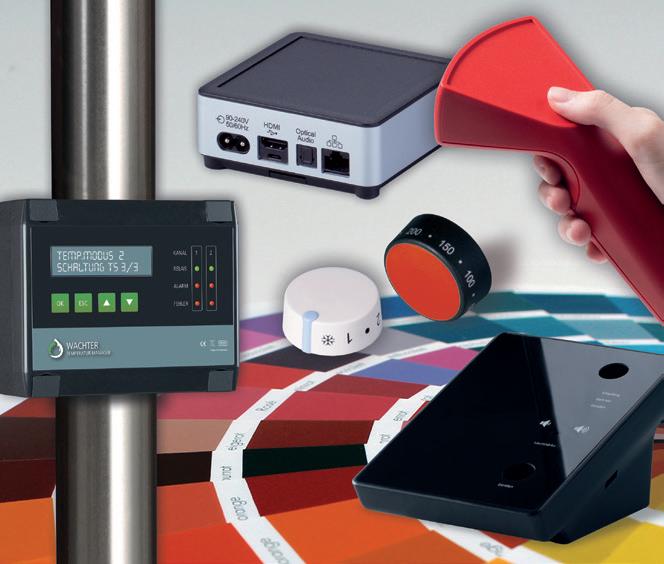
Possible processing options include milling, thread tapping, engraving, drilling, countersinking, sawing or punching. Individual machining options, ranging from prototype production to series-type production, can also be carried out quickly.
Colour and surface finishes such as corporate identity colours, soft-touch coatings, metallic effects, gloss levels and ESD coatings are available.
Labelling and marking are carried out using laser marking, screen, tampo or digital printing — as well as all-round printing (for tuning knobs). Possible options include QR codes, sequential numbering, colour gradients, and fluorescent or luminescent colours.
For EMC protection (electromagnetic compatibility), the inside of the enclosure can be coated with 99.98% pure aluminium. Production in special colours is also possible – for this purpose, the natural material is extruded and coloured according to a sample or a RAL or Pantone colour chart.
In the field of assembly and finishing, OKW can, on request, take care of tasks such as screw fitting, bonding or installing accessories. In addition, a wide range of fasteners is available, such as threaded bushes, spacers and fastening pillars.
The concept of modifiable standard enclosures combines the advantages of standard components with individual design. The result is custom-fit, ergonomic and high-quality devices that are innovative, safe and ready for use.
ROLEC OKW AUSTRALIA NEW ZEALAND P/L www.okw.com.au
faster, more efficient flexible electronics by identifying how much softness is too much.
“There may be a glass ceiling on how well flexible molecular materials can conduct electricity,” Venkateshvaran said. “If we understand the relationship between stiffness and charge transport, we might find ways to push past it.”
This is a modified version of a news item published by the University of Cambridge under CC BY-NC-SA 4.0. This version is similarly licensed under CC BY-NC-SA 4.0.
In the fast-evolving landscape of industrial automation, the Ditel Micra M Max digital panel meter is designed to enhance how users interact with process data. The ‘Max’ iteration of the digital panel meter prioritises wireless technology and seamless connectivity with the integration of Bluetooth.
Traditionally, configuring a digital panel meter required physical access, specialised cables, or complex menu navigation via front-panel keys. The Micra M Max breaks these barriers through the Ditel Connect mobile app. Engineers can now configure devices wirelessly via smartphone, thereby reducing setup time in hard-to-reach areas. The digital panel meter also enables engineers to export and clone configuration files, for consistency across multiple units on a factory floor.
Beyond local setup, the digital panel meter leverages MQTT (Message Queuing Telemetry Transport) protocols to bridge the gap between hardware and the cloud. This allows for automatic, real-time data transmission to central servers every minute, effectively turning a standard panel meter into a sophisticated IoT edge device. By removing the need for extensive wiring for data logging, Ditel has simplified the path to predictive maintenance and advanced asset management.
For those who prefer a desktop environment, the integrated web server allows users to monitor live readings and program tasks directly from a web browser — no additional software required.
The digital panel meter has also retained its signature tri-colour programmable LED display and supports a range of inputs, from temperature (Pt100, thermocouples) to process signals (mA, V) and load cells. The display range has also been extended to 99,999 points, providing higher resolution for critical measurements.
CONTROL DEVICES AUSTRALIA www.controldevices.com.au
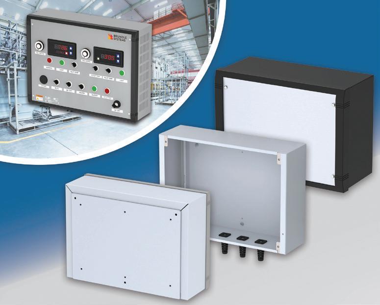
The DATAMET wall mount enclosures from METCASE are suitable for the HMI electronics field, as well as for control and instrumentation applications.
These smart, modern aluminium enclosures are designed for factory processing, security, machine control, measurement and detection. They are a cost-effective alternative to METCASE’s premium TECHNOMET-CONTROL, which is designed for VESA mounting.
DATAMET offers complete access to the electronics during installation and servicing. First the L-section rear panel is attached to the wall; there are four pre-punched mounting points. Then the top section, front bezel and front panel (accessory) are added. All the fixings are supplied with the case.
The rear section includes holes for installing PCBs and internal mounting plates. The front panel is recessed in the diecast front bezel to protect controls. Inside, there are four M4 earth studs.
DATAMET can be specified in three sizes: S (250 x 180 x 116.5 mm), M (350 x 250 x 116.5 mm) and L (400 x 300 x 116.5 mm). There are two standard colour schemes: light grey/window grey (RAL 7035/RAL 7040) and black (RAL 9005). Custom colours are also available on request.
Accessories include front panels, mounting plates, a PCB mounting kit and PCB/ panel fixing screws.
METCASE can supply DATAMET fully customised. Services include bespoke sizes, custom front panels, machining, fixings and inserts, painting and finishing, and photo-quality digital printing of legends, logos and graphics.
ROLEC OKW AUSTRALIA NEW ZEALAND P/L www.metcase.com.au
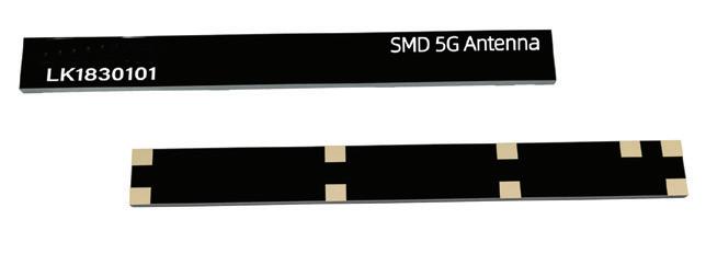
Leankon has released the LK1830101 (5G) and LK1830201 (4G LTE) ultraslim SMD antennas, engineered for the spatial constraints of next-generation IoT applications. Featuring a 1 mm profile, these surface-mount components allow designers to maintain sleek product aesthetics without compromising wireless reliability.
The series is purpose-built for global deployments, supporting an expansive frequency range of 600–960 MHz and 1400–6000 MHz. This wideband coverage enables seamless compatibility across 5G, 4G LTE, LTE CAT-M and NB-IoT, eliminating the need for regional hardware variants. Beyond cellular connectivity, the antennas support precision multi-constellation positioning (GPS, GLONASS, Galileo and BeiDou L1), making them suitable for fleet management, asset tracking and industrial automation.
The antenna’s 1 mm height facilitates integration into space-constrained wearables and industrial sensors.
The antennas also feature omni-directional radiation, for consistent signal coverage regardless of device orientation. Their SMD form factor is designed for automated pick-and-place assembly to reduce manufacturing costs and accelerate scaling.
To streamline the design-in process and reduce time-to-market, Leankon is offering free samples and evaluation boards for rapid performance validation.
LEANKON www.leankon.com
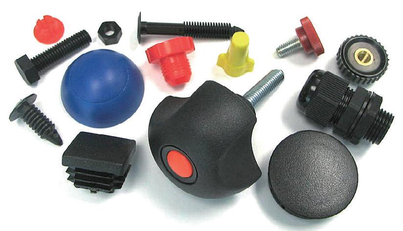
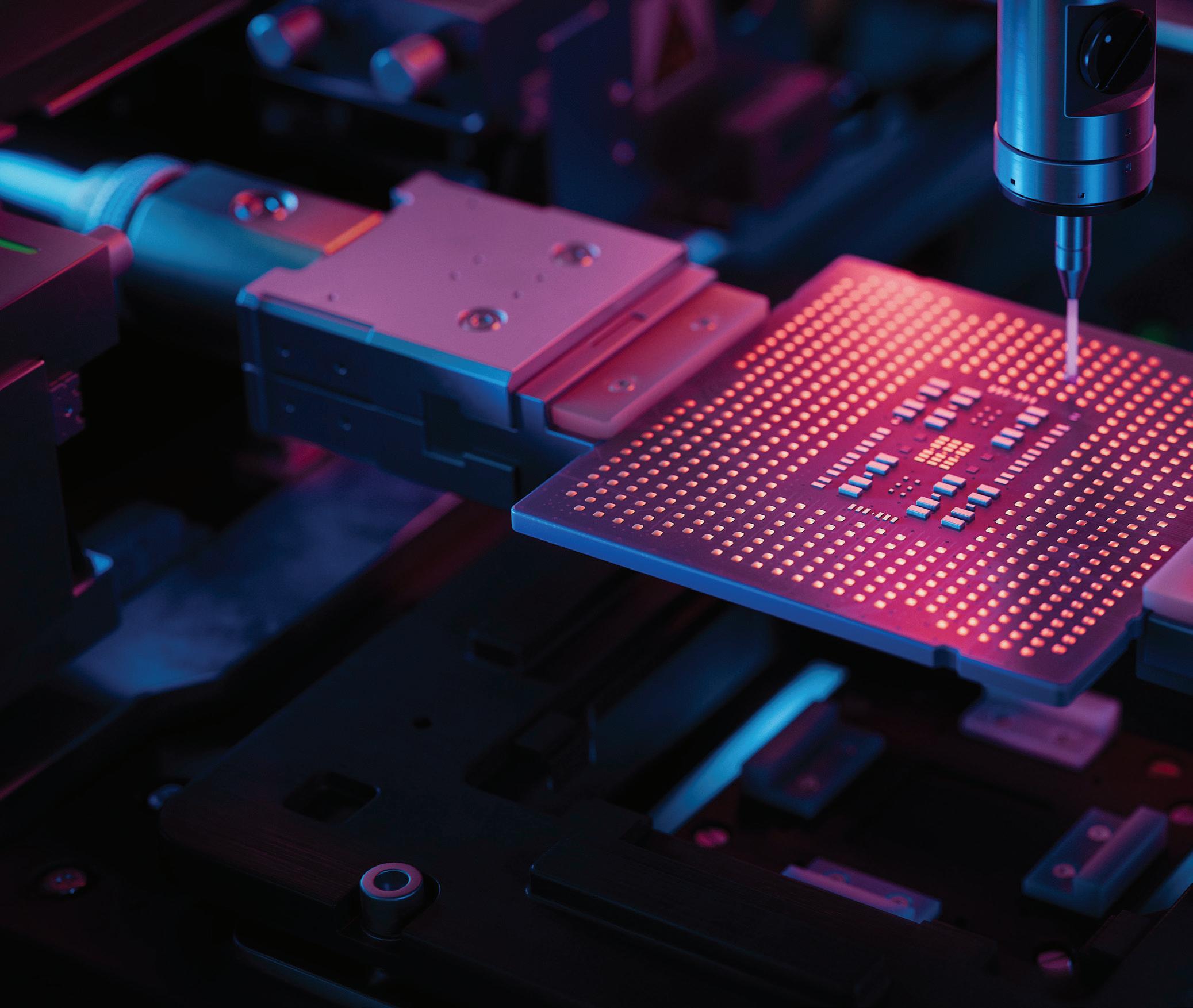
David Nutt, Cornell University
CORNELL RESEARCHERS HAVE USED HIGH-RESOLUTION 3D IMAGING TO DETECT THE ATOMICSCALE DEFECTS IN COMPUTER CHIPS THAT CAN SABOTAGE THEIR PERFORMANCE.
The imaging method, which was the result of a collaboration with Taiwan Semiconductor Manufacturing Company (TSMC) and Advanced Semiconductor Materials (ASM), could touch almost every form of modern electronics, from phones and automobiles to AI data centres and quantum computing.
The research findings have been published in Nature Communications. The lead author is doctoral student Shake Karapetyan.
“Since there’s really no other way you can see the atomic structure of these defects, this is going to be a really important characterisation tool for debugging and fault-finding in computer chips, especially at the development stage,” said David Muller, the Samuel B. Eckert Professor of Engineering in the Cornell Duffield College of Engineering, who led the project.
Tiny defects have been a long-standing challenge for the semiconductor industry, especially now, as the technology has grown increasingly complex while the components
have shrunk in size to the atomic scale.
The focus of the study, and the heart of the computer chip itself, is the transistor: the little switch through which electrical current flows via a channel that gets opened and shut by an electrical gate.
“The transistor is like a little pipe for electrons instead of water,” Muller said.
“You can imagine, if the walls of the pipe are very rough, it’s going to slow things down. So measuring how rough the walls are and which walls are good and which walls are bad is now even more important.”
Muller has a unique insight into the design of semiconductors. From 1997 to 2003, he worked in the research and development division of Bell Labs — where transistors were invented — exploring the physical limits that dictate just how tiny a transistor could get.
After their introduction in the mid-20th century, transistors were initially built like suburbs: flat and sprawling outward, according to Muller. Over time, as the chips ran out of horizontal real estate, designers
started to stack transistors vertically, in three dimensions, like apartment blocks.
“The problem is these 3D structures are smaller than the size of a virus. And these days, it’s a lot smaller. It’s more like a molecule-in-the-cell kind of scale,” Muller said.
A single high-performance chip can now contain billions of transistors. But as they’ve shrunk in size, the technology has become more difficult to troubleshoot.
“These days, a transistor channel can be only about 15 to 18 atoms wide, which is super, super tiny, and they’re extremely intricate,” Karapetyan said. “At this point, it matters where every atom is, and it’s really hard to characterise.”
At Bell Labs, Muller and fellow scientist Glen Wilk, who is now vice president of technology at ASM, tried replacing silicon dioxide — the prevailing gate material, which leaked too much current at small scales — with hafnium oxide. Within a few years, Muller and Wilk departed Bell Labs, but their work continued to reverberate with semiconductor
companies, and hafnium oxide soon became the industry standard for computers and mobile phones in the mid-aughts.
“The papers we published on how to use electron microscopes to characterise these materials, I can tell you, a lot of the semiconductor folks had read those very, very carefully,” Muller said. “When we got back into this project, that was very clear. And the microscopy has gone a very long way. Back then, it was like flying biplanes. And now you’ve got jets.”
The jet, in this case, is electron ptychography, a computational imaging method in which an electron microscope pixel array detector (EMPAD) — a technology co-developed by Muller’s group — is used to collect detailed scattering patterns of electrons after they pass through the transistors. By comparing how these patterns change from one scan position to the other, scientists can reconstruct an image with extraordinary clarity. The detector is so precise, it has enabled the highest resolution images in the world,
showing atoms in unprecedented detail, as recognised by Guinness World Records.
‘Mouse bites’
More than 25 years after their last joint project, and with the support of TSMC and its Corporate Analytical Laboratories group,
Muller’s team and Wilk decided to collaborate again and use the EMPAD to peer inside modern semiconductors.
“You can think of this imaging technique like solving a massive puzzle, both in terms of taking the experimental data and doing the computational reconstruction,” Karapetyan said.
When all the data was collected and reconstructed, and the position of atoms had been tracked, the researchers were able to detect interface roughness in the channels — revealing what Karapetyan termed “mouse bites.” The roughness arose from defects that formed during the optimised growth process. Sample structures, grown at nanoelectronics hub Imec, were the ideal way to test the imaging method.
“Fabrication of modern devices takes hundreds, if not thousands, of steps of chemical etching and deposition and heating, and then every single step does something to your structure,” Karapetyan said. “Before you used to look at projective images to try to figure out what was really going on. Now you have a direct probe to actually see after every single step and have a better grasp of, oh, I put the temperature this high, and then this is what it looks like.”
The new imaging capability could potentially impact almost anything with a modern computer chip, from mobile phones to laptops and data centres, and could be a boon for debugging next-generation technologies such as quantum computers, which require extraordinary structural control of materials that is still not fully understood.
“I think there’s a lot more science we can do now, and a lot more engineering control, having this tool,” Karapetyan said.
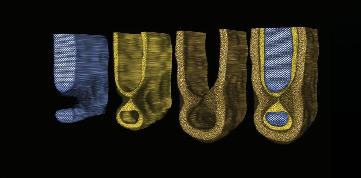

University of Sydney
AUSTRALIAN RESEARCHERS HAVE BUILT AN ULTRA-COMPACT ARTIFICIAL INTELLIGENCE (AI) CHIP THAT IS ABLE TO MAKE CALCULATIONS USING THE POWER OF LIGHT, AT THE SPEED OF LIGHT.
The nanophotonic chip prototype, which harnesses the power of light particles (photons) is built completely in-house at the Sydney Nano Hub at the University of Sydney.
The researchers say the prototype could play an important role in developing more energy-efficient AI hardware as global demand for artificial intelligence continues to grow, potentially lowering the overall energy footprint of future computing systems.
Traditional computer chips use electricity to process information, which means moving tiny, charged particles (electrons) through wires. This produces heat.
The nanophotonic chip prototype uses light. Light can travel through materials without electrical resistance, so it does not generate heat in the same way electricity does. As the light passes through the nanostructures within the chip prototype, these structures themselves perform the calculation automatically.
The nanostructure on the chip takes up tens of micrometres, roughly comparable to the width of a human hair. The nanostructures together help form a neural network: artificial neurons that mimic the human brain to recognise and complete calculations.
The prototype performs calculations on the picosecond timescale, or trillionths of
a second — the time it takes light to pass through the nanostructure.
The researchers say the advantage of using photonics is the computation is much faster, taking place at the speed of light. The technology also uses light to operate instead of electricity. This is compared to current data centres that rely on massive amounts of water and energy to power them.
“We’ve re-imagined how the photonics can be used to design new energy-efficient and ultrafast computer processing chips,” said Professor Xiaoke Yi. “Artificial intelligence is increasingly constrained by the energy consumption. This research performs neural computation using light, enabling faster, more energy-efficient and ultra-compact AI accelerators.”
Published in Nature Communications, the study demonstrates how AI models can be designed into nanoscale photonic structures that manipulate light to perform the mathematical operations required for machine learning.
To validate the technology, the researchers trained the nanophotonic chip to classify more than 10,000 biomedical images such as breast, chest and abdomen MRI scans.
In simulations and experiments, the nanophotonic neural network achieved approximately 90–99% classification accuracy.
The technology offers a pathway to sustainable AI infrastructure capable of supporting the growing demands of computing without proportional increases in power consumption.
Photonics, short for photon-based electronics, is the study of controlling light particles. It has been used to power technology we use day-to-day, such as lasers, fibre-optic networks and in medical imaging.
But photonics being harnessed for computer processing has only been explored in recent years, with increasing urgency with the rise of AI demand.
PhD student Joel Sved, who played a key role in design and implementation of the prototype, said the prototype shows how intelligence can be embedded directly into nanoscale photonic structures.
For more than a decade, the Photonics Research Group at the University of Sydney has had a long history of studying how to push the limits of photonics including to improve our technology.
This includes using photonics to tackle challenges in wireless communications and advanced sensing technology which can detect and measure chemical or biological traces in the environment.
Following the successful testing of the nanophotonic chip prototype, Yi’s team is now working on advancing the technology towards larger-scale photonic neural networks.