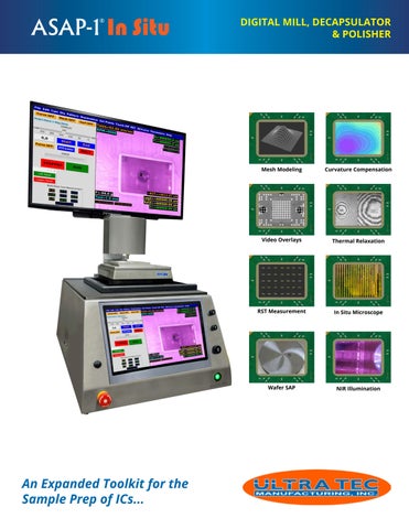
ASAP-1 In Situ
DIGITAL MILL, DECAPSULATOR & POLISHER
Mesh Modeling
Curvature Compensation
Video Overlays
Thermal Relaxation
RST Measurement
In Situ Microscope
300mm Ready
Wafer SAP
An Expanded Toolkit for the Sample Prep of ICs...
NIR Illumination
NEW FEATURES
ENHANCED VIDEO
Building on more than 25 years of product development and customer input, ASAP-1® In Situ is our flagship benchtop milling, decapsulation, and sample prep system. ASAP-1® In Situ includes a new OS, driven by a large touchscreen and/or mouse & keyboard — or even programmed remotely — that allows for control of all process parameters. Stage illumination has been further improved, with the addition of NIR LEDs. Three standard UHD cameras (target, front & side process) ensure the process can be monitored live. An ‘open’ physical design allows ASAP-1® In Situ to successfully process the widest size range of IC package — from the tiniest surface mount components, right up to the largest aerospace modules/motherboards and selected areas of a 300mm wafer. Along with legacy thermal, end-pointing and curvature compensation options, ASAP-1® In Situ can be fitted with a through-silicon RST Measurement System — allowing in situ mapping of remaining silicon across the die without sample transfer — thus avoiding translation errors.
Image Overlays
ASAP-1 In Situ Advanced In Situ Imaging Three UHD cameras are fitted as standard. A fourth camera is added with an RST upgrade.
45° Process Front
Camera Options
45° Process Side
Target Camera
Microscope Camera (Option) @ RST Position
Enhanced Stage Illumination An array of controllable visible light LEDs illluminate the stage area. We have recently added NIR LEDs to enhance backside visibility during final processing.
X-Ray
NIR illumination can also assist with viewing underfill and epoxy materials.
Target Cam
X-Ray Overlaid onto Target Cam Image
The live Target Cam view can be overlaid with saved X-Ray, C-Sam, a previously saved part, or bonding/ design images to further improve targeting. Image manipulation, such as scaling and rotation, can be made with the In Situ software.
2
Visible LEDs
NIR LEDs
On an ultrathinned die, the visible LEDs start to reveal circuitry (shown left). With NIR Illumination, circuitry can be seen in the complete thinned area.
NEW FEATURES
ASAP-1 In Situ
FLUID CONTROL & RST
Fluid Control System (FCS) Available for dispensing and collection of polishing fluids, abrasives, and lubricants. Effective control of lubricants and particulates greatly improves the quality of live process visual monitoring.
The acclimation plate ensures that fluids are dosed to the tool/die interface at the correct temperature.
In Situ Through-Silicon RST Measurement Options
VIS
NIR
Code
Spectrometer
Minimum RST Measurement
Application
UT-F3
NIR
8 microns
Standard thinning
UT-VIS
Visible Light Extension
8 nanometers Ultrathinning
(<10 microns)
Two In Situ options are available for measuring and mapping remaining silicon thickness (RST). For standard thinning and polishing applications, the single NIR (UT-F3) Spectrometer is applicable. For applications that require ULTRATHINNING, to below 10 microns RST, the additional visible light (UT-VIS) spectrometer should also be purchased.
Pocket Area Mesh
Whole Die Mesh
Mesh overlaid onto the measured package curvature profile
3
USING CURVE & MESH MODELS
ASAP-1 In Situ
Working with Curved & Warped Die Die warpage occurs due to mismatch in the coefficient of thermal expansion (CTE) between the various components used in the manufacture of semiconductor packages. Complex models exist to predict stresses, however a straightforward analogy is to view warpage as resembling a bimetallic strip. The degree of warpage varies widely part-to-part, manufacturer-to-manufacturer and even batch-to-batch. A BGA’s warpage is generally convex (‘frowning silicon’) at ambient temperature, with the convexity often increasing further as the silicon is thinned. Curvature models that can be applied throughout the thinning process to maximize uniformity across the die.
The System OS provides the user with Interactive Plots to compare the Actual RST map to the adapative 3D Curve Model. Thickness variations are nullified during the thinning process by using a combination of 3D Curvature measurements and RST map, overlaid with an adaptive Mesh. Through subsequent polishing iterations — with attendent modifications of the Mesh Model — the ACTUAL sample thickness and uniformity converges with the final requirement after final polishing.
Tilt & Curvature Measurement Initial Measurement
After Tilt-Table Auto-Align
The Auto-Tilt function physically measures a five-point or nine-point matrix to measure tilt and package curvature in X and Y. Another new feature is the measurement of a device’s Flex during touch-off measurement procedures. Flex is an indicator of the quality of sample mounting and/or the seating of a board-level component.
4
ASAP-1 In Situ
TYPICAL ULTRATHIN & POLISH SEQUENCE
A Starting Point -
B Process Mid-Point
Final Thinning C Standard (~50 microns to ~20 microns RST)
(50-100 microns RST)
Initial Thinning
3mm Tool Model Target Camera View of Die @ 50 microns +/- 5
Large Flip-Chip BGA package Initial die thickness = 750 microns
Contour Map of RST Points
Thinning Process Conditions Die size X = 15 mm Y = 10 mm 5260.3 3mm dia fine diamond tool Spiral polishing pattern Thermal relax at 80°C Curvature compensation Tool force = 300g
D Ultra Thin and Polish - Adaptive (~20 microns to ~5 microns RST) Curvature + Mesh Model
Note: The map selected has calculations for tool convolution to minimize radius error.
Process Conditions Graphical Plot of RST
5260.3 3mm dia fine diamond tool 5265.3 3mm dia superfine diamond tool Mix of Spiral and ASAP-1® polishing patterns Curvature compensation Polishing force = 300g
E Final Results
Curvature + Refined Mesh Model
Ultra Thinned Die Final thickness = 5 microns +/- 1
Note: Additional polishing passes may be required. RST is measured and the 3D mesh is refined after each cycle. Final RST Map
Process Conditions 5295.3 3mm dia Xylem tool 2382.5 blue diamond paste 2385.5 yellow diamond paste ASAP-1® series polishing patterns Polishing force = 300g Final polish with 5299.3 Xybove 3mm tool with colloidal silica/alumina
Target camera image of final 5 micron RST surface Examples of Ultrathinning
Typical Process Time = 1 to 4 hours Note: For ultimate thinning requirements, the final process is extended in D. Shown right are die thinned to 1 to 2 microns RST.
5
ASAP-1 In Situ
LEGACY UPGRADES Thermal Relaxation In Situ thermal modification of the packaged device, during sample prep, has been long proven as a safe and effective tool to optimize the ultimate silicon die uniformity. Thermal relaxation can be used either alone, or more frequently in conjunction with supplementary methods such as Curvature Compensation and 3D-Mesh. The Thermal Stage (6686.1) is a standard upgrade It also incorporates a Hot Plate Mode for sample mount/demount with Crystal Wax. Moiré patterns on identical devices prepared at increasing temperatures show an increase in final thickness uniformity.
A chiller cools the stage and adds system thermal stability
End-Point Techniques In addition to a range of TIME and PRESSURE based process endpoints, ASAP-1® In Situ offers a unique suite of Capacitance/ Resistance-derived, ELECTRICAL End-pointing features. By grounding the part to the end-point stage, the capacitive build-up between the approaching electrically-live diamond tool and an embedded feature of interest (die circuitry, bond wires) can be used as the automatic trip for a decap process. Use of the method allows for fast, accurate and repeatable process end-points to be achieved without the need for time consuming visits to/from an optical microscope.
Microsurgery with a live 0.4mm dia mill in combination with a probe tip
6
‘Breadboard’ used to ground the pins of a DIP for decap with electrical endpoint
Decapped Plastic Package
Bond Wire
Circuitry
ASAP-1 In Situ
CORE SYSTEM SPECIFICATIONS
Feature
Specification
Z-Vertical Direction Precision
0.04 microns (40 nanometers) minimum step-size
Table Precision (X & Y Travel)
0.2 microns (200 nanometers) minimum step-size
Table Travel Amplitude
100mm x 100mm (max.)
Polishing Method
Patented ASAP-1® Float-down head, with Z-lock, enhanced with electronic sensors and tool patterns (ASAP-1® Classic, ASAP-1® X, ASAP-1® Swap, Serpentine, User-defined X-Y, Spiral, Frame, and Relief)
Sample Tilt Control
Automated 2-circle stage tilt control (+/- 5 degrees)
Force Control
1000 grams (max) with 1gram precision. Overall accuracy +/- 10 grams
Video
Realtime 10.1inch (255mm) touchscreen monitor, overlaid with stage and process variables. HDMI Video-Out for (optional) external monitor. 4.25inch (108mm) secondary touchscreen
Programming Input Method
Touchscreen, joystick and 3 physical rotary encoders. Optional wireless keyboard and mouse. File load/save to flash drive. Remote programming
Core Software Features
Drop-down menu interface for File handling, Cam Select, zoom, and image enhancement, Overlays, Tool Diameter, Pattern Select, Force Control, timers, Illumination, Set-points, Touch-off. Additional purchased options unlock menus for RST, 3D controls, thermal, end-point
Process Cameras
Two 4K UHD Cameras provide real-time video at 45 degrees to tool/surface interface at front and side
Target Camera
4K UHD Camera provides top-down video for positional targeting
Power Requirements
Universal: 100-120VAC; 200-240VAC (Single Phase). Power Consumption: 300 Watts Maximum in use
Footprint
19 inches (480mm) Width x 27.5 inches (698 mm) Depth x 27 Inches (685mm) Height
Weight
200lbs (91 kg)
ORDERING INFORMATION Code
Item
Description
6760.5
ASAP-1® IN SITU (2025 Model)
DIGITAL Selected Area Preparation System, (100-240V, 50/60Hz). Includes: tool spindle drive with sub-micron Z-resolution, +5/-5 degree automated X-Y tilt-table, integrated real-time machine vision, min 10-inch touchscreen lcd monitor, set of 2mm and 3mm tools, 6389.1 Force Feedback module. Three 4K UHD Cameras (Target & Process Front and Side)
6394.3
3D Module - Curvature & Mesh
System software upgrade to add processing and compensation for sample surface curvature with adaptive mesh overlay
6686.1
Heat & Cool Thermal Relaxation Stage
Hardware and Software Upgrade to add thermal relaxation capability. Touch-Panel screen controls. Peltier-based heating plate, Chiller unit. Includes cables, and two mounting plates. Hot Plate Mode
6675.1
Machine Vision Monitor
24-inch (min) monitor machine vision upgrade for improved In Situ view of polishing tip/sample surface interface, includes stand (VESA mount)
6677.1
Fluid Control System (FCS)
Auto dispense and collect system for polishing fluids and abrasives. Three input lines
6682.1
Thermal Acclimation Plate
Adds ability to allow inlet fluid from FCS to reach required process temperature
UT-F3
RST (Through-Silicon) Measurement System
Non-contact measurement (1280-1340nm) of silicon and other semiconductors. Includes: Thickness-Solving Software. 4K Video camera (microscope); Si thickness standard. Note: Customer supplies own PC/tablet – Windows 10 required. Measures from full wafer thickness down to approx. 8 microns RST
UT-VIS
VIS Extension for thin films
2nd “VIS” Spectrometer addition to the UT-F3 system to allow for ultra thinning applications. Adds film measurement down to approx. 8nm RST
6368.1
Capacitive/Resistive EndPoint Module
Hardware and Software Upgrade to add end-pointing for enhancement of decapsulation performance
Characterization Modules
7
ASAP-1 In Situ
APPLICATIONS ARRAY
Small Devices
Stacked Die
Smart Cards
Large Modules/Motherboards
BGA Reveal
Cross-Sectioning
Ultrathinning
Decapsulation
Stacked Die
Die Removal
Chip Off
Power Devices (SiC, SiN, Si)
Wafers (200 & 300mm ready)
Multi-Chip Modules
Ceramics
De-Processing
Ask how we can help with YOUR application Polishing Technologies, Helping Your Lab to Shine... ULTRA TEC is proud to operate a continuous product improvement program. Product specifications and appearance are subject to modification without prior notification. Note: ASAP-1® is a Registered Trademark. Portions of the Technology are covered under US and related Worldwide patents - 6,630,369; 6,781,232; 7,066,788; 9,157,935 & 6,245,586. More patents are pending. All other trademarks remain with original trademark holders. Fall 2025 Edition
Toll Free (US) 1-877-542-0609 Tel: +1-714-542-0608 Fax: +1-714-542-0627 1025 E. Chestnut Ave., Santa Ana, CA 92701-6425, USA Email: info@ultratecusa.com www.ultratecusa.com