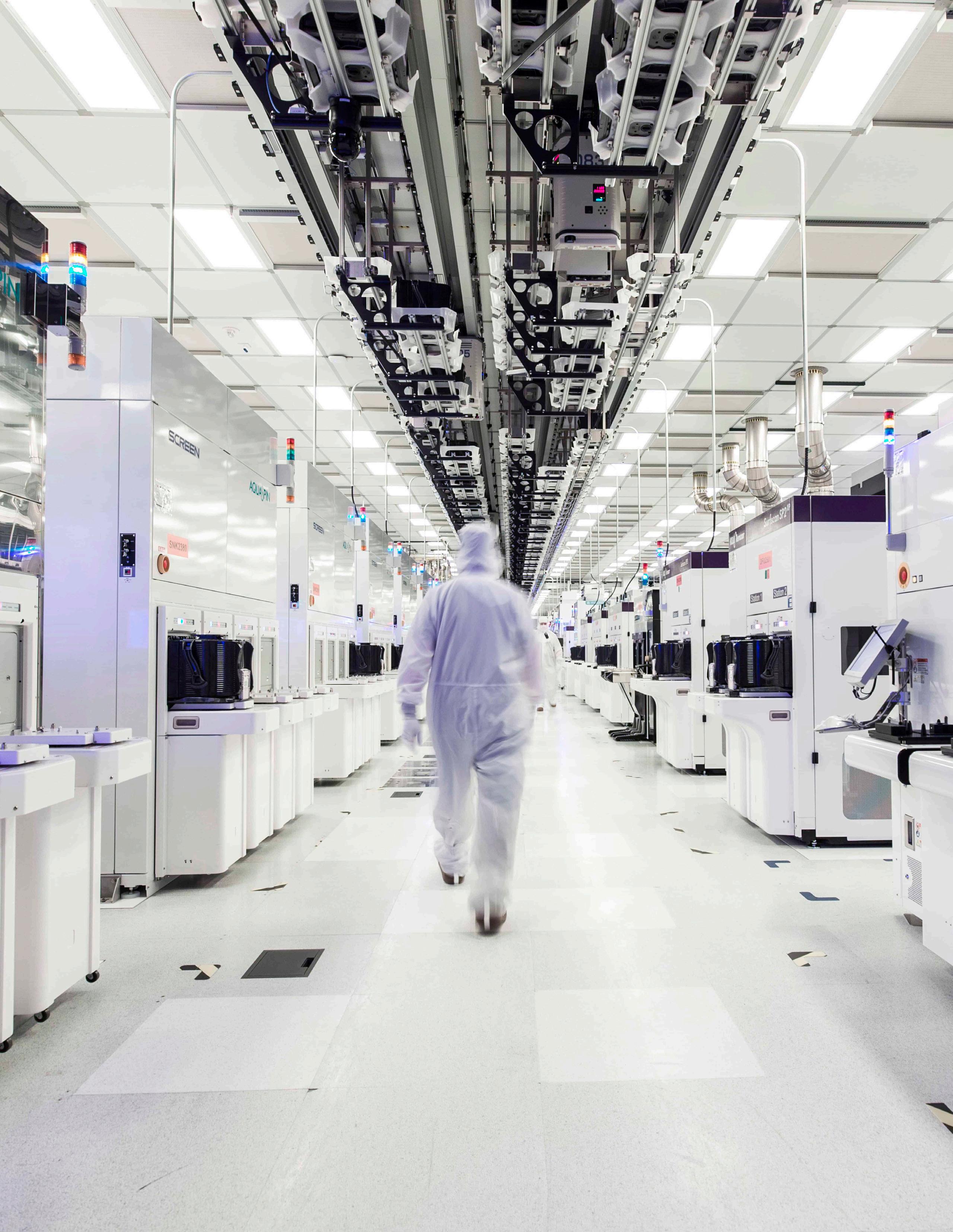
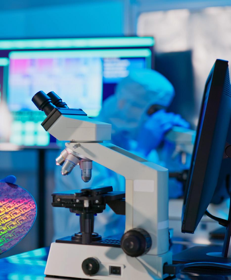
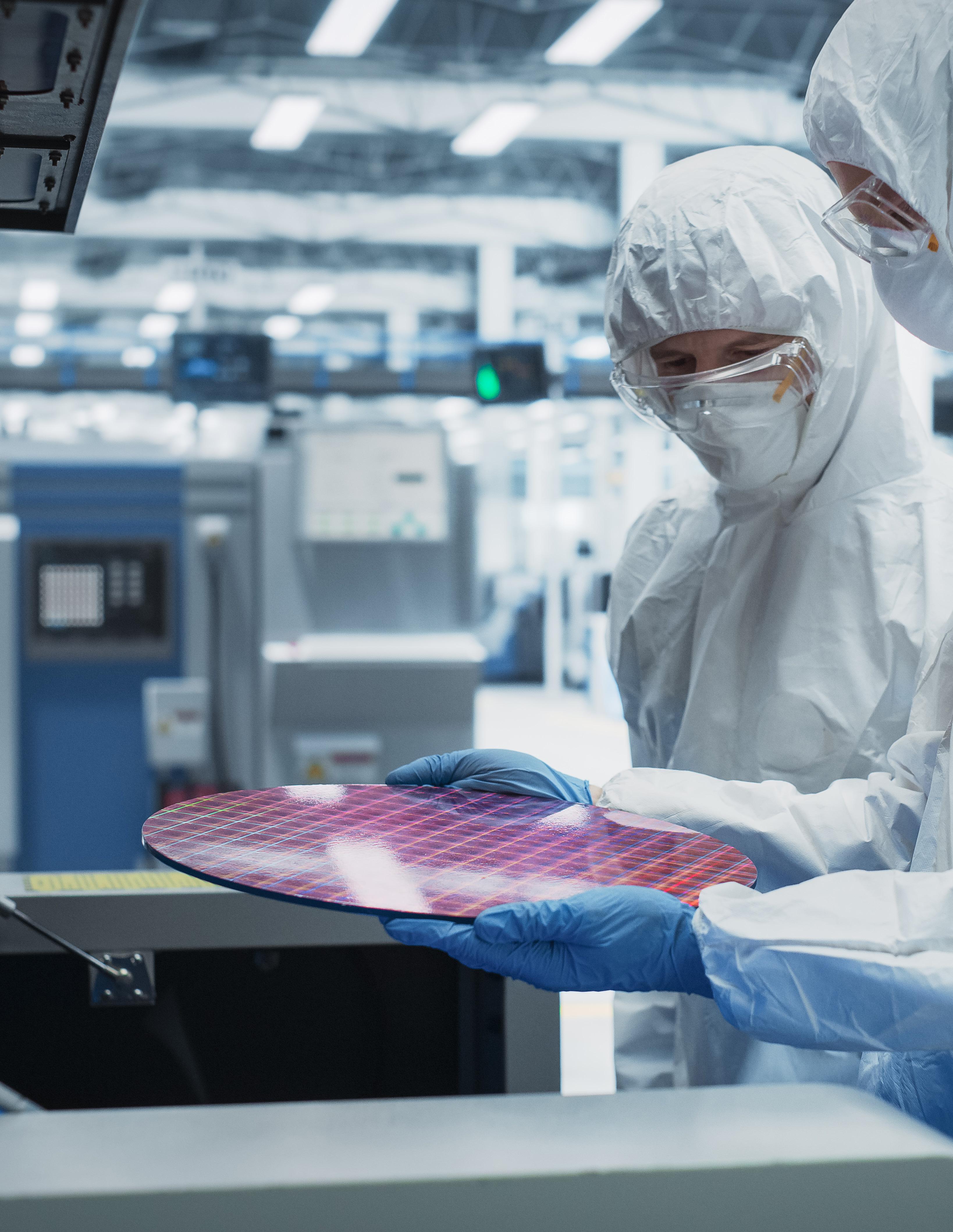
Semiconductors Advanced Manufacturing
Designing tomorrow’s innovations
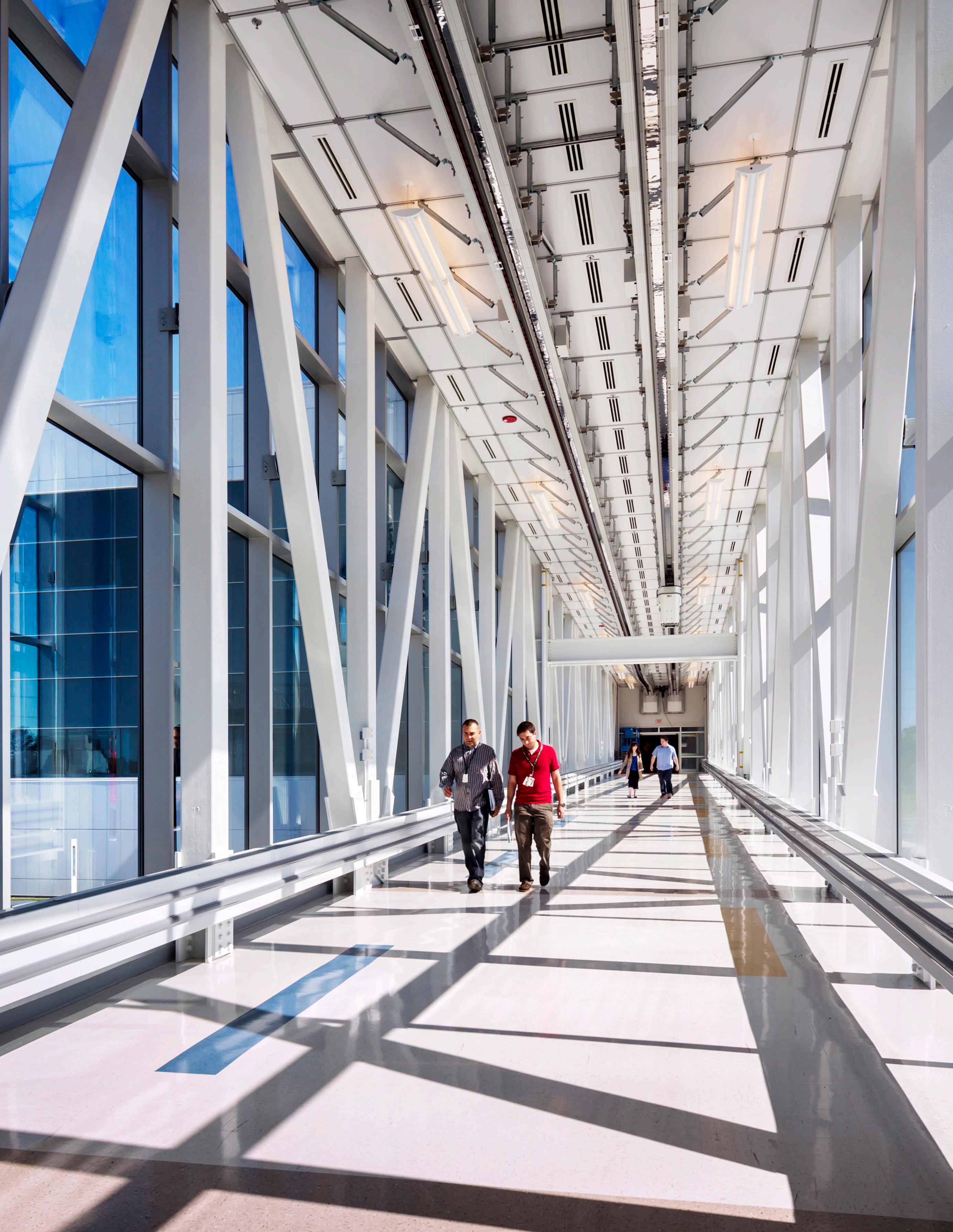
Manufacturing is evolving—driven by automation, data, and engineering breakthroughs. Page partners with industry leaders in semiconductors, electric vehicles, energy storage, and more to design leadingedge facilities, from cleanrooms and tool hookups to process utilities and water/wastewater management.
Ranked among the top 10 in manufacturing and semiconductor facility design, we create solutions that enhance precision, efficiency, and sustainability. Whether shaping lithium battery production, solar advancements, or next-gen automotive manufacturing, our expertise keeps clients ahead of the curve— ensuring facilities perform at the highest level today while remaining adaptable for the future of production, research, and development.
We design and engineer highperformance semiconductor and manufacturing facilities that drive innovation, optimize production, and accelerate time to market for the world’s most advanced industries.
Automotive
Cleanrooms
Electric Vehicles
Energy Storage
Facility Planning
Lithium Battery
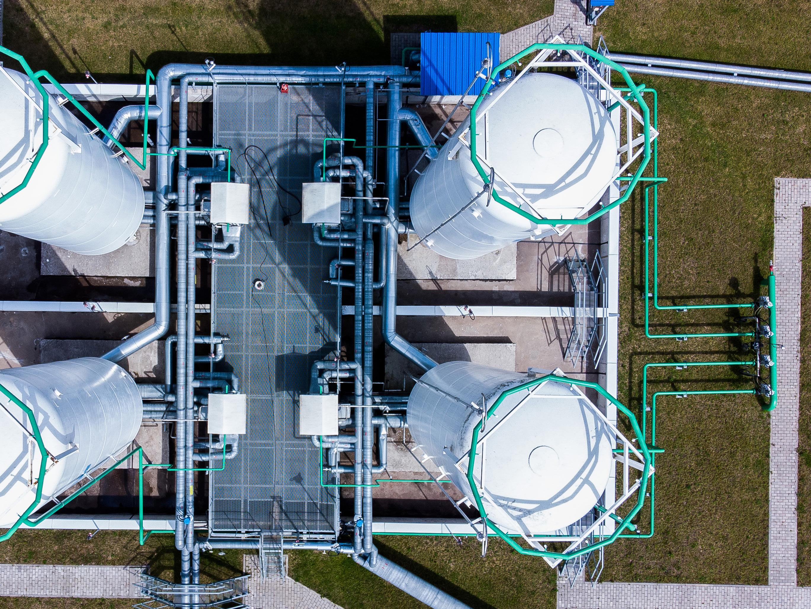
Process Utilities
Semiconductor
Solar
Tool Hookup
Water / Wastewater


Semiconductors

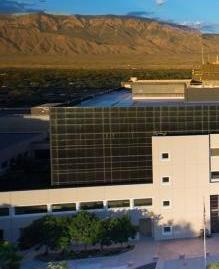
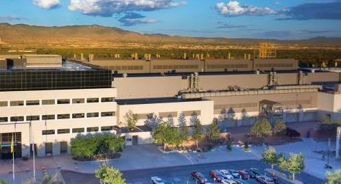
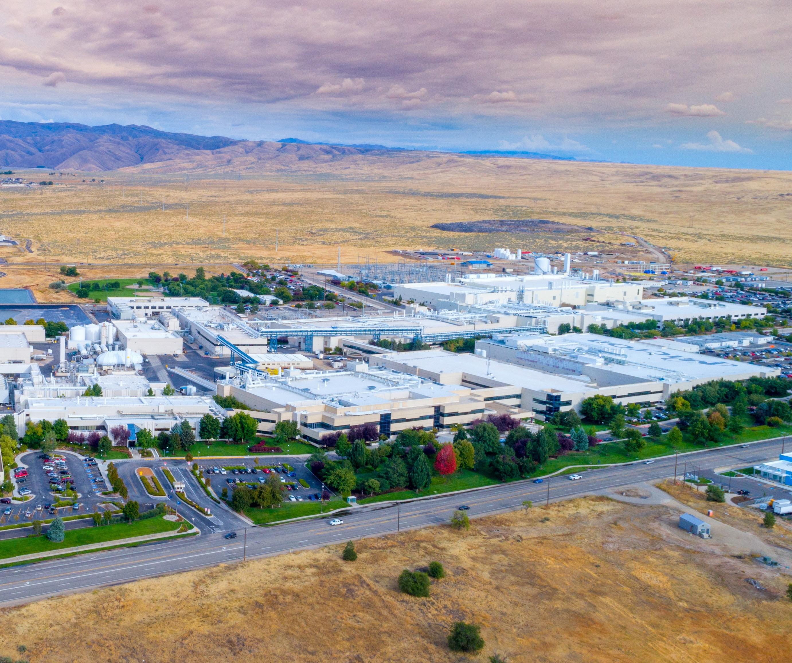
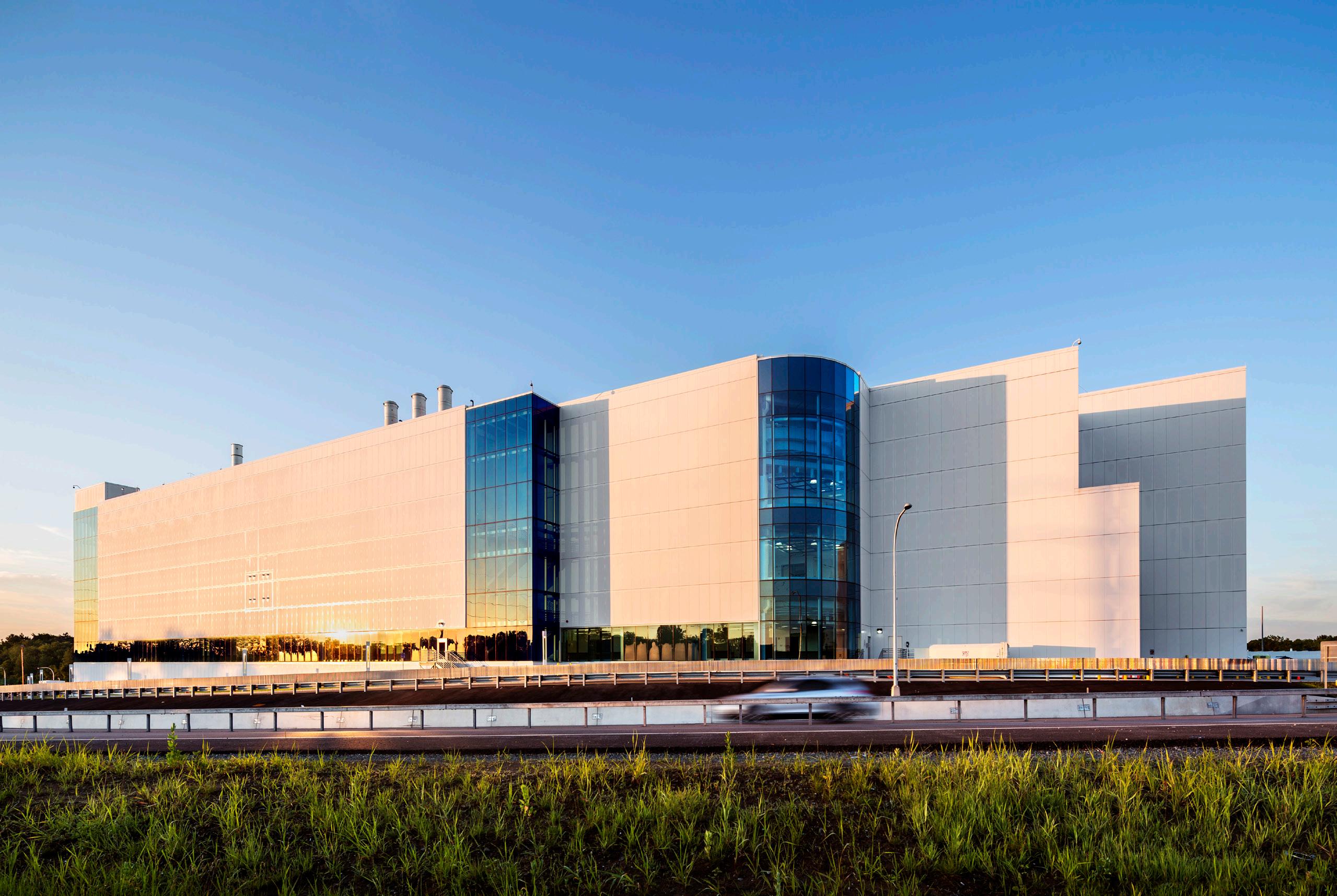
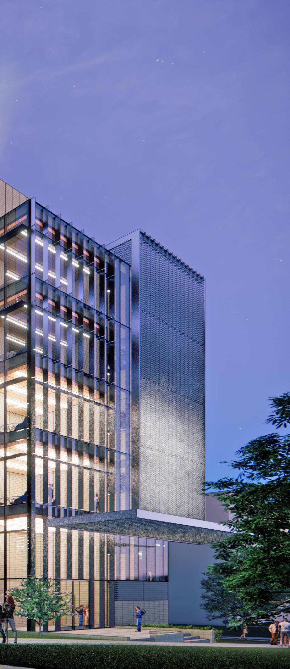
Confidential Wafer Manufacturer Building A
Phase 1
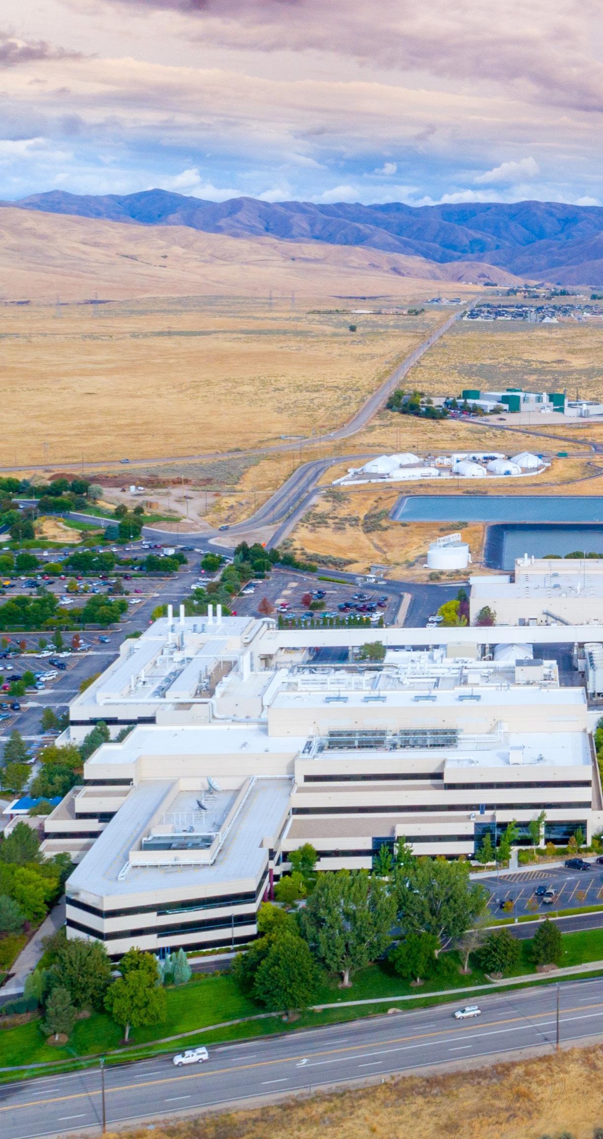
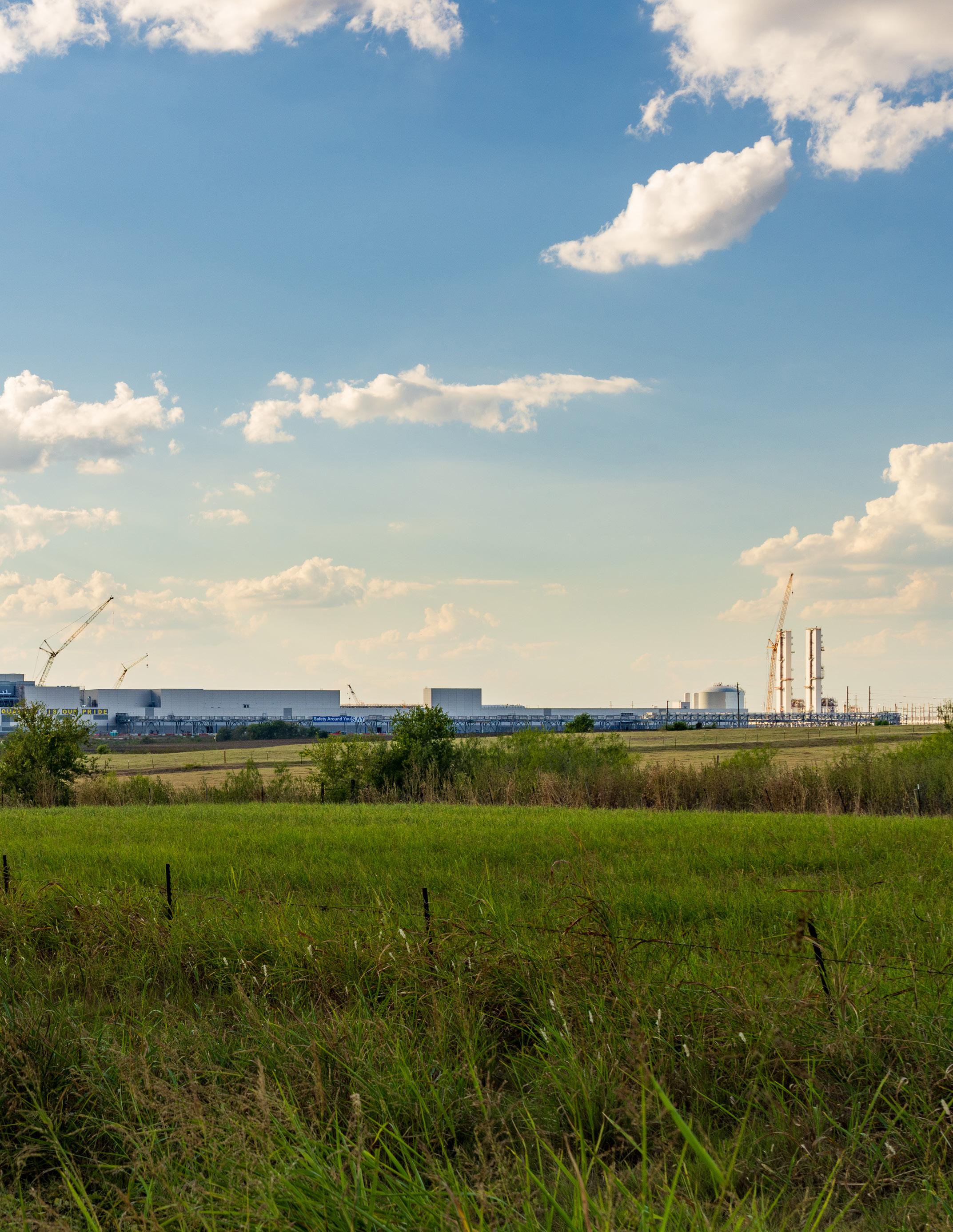
A new 300-millimeter silicon wafer manufacturing facility in North Texas represents a major advancement for the semiconductor industry and the regional economy. As the foundation of modern electronics, silicon wafers are essential to semiconductor fabrication. However, with the majority of wafer production occurring overseas, the U.S. has faced longstanding supply chain vulnerabilities.
This facility is the first of its kind in over 20 years, closing a critical gap in domestic manufacturing. By bringing wafer production back to the U.S., it strengthens supply chain resilience, reduces reliance on imports, and fuels innovation. This factory is a strategic investment in America’s technological leadership, ensuring the nation remains at the forefront of semiconductor advancements.
Services Provided
Architecture / Interior Design / MEP Engineering / Structural Engineering (Admin Bldg. & Central Utilities Building) / Commissioning
Relevancies
Fab / Central Utility Plant (CUP) / Admin Building / Water-Wastewater Treatment / Warehouse / Cleanroom
Services Provided
Architecture / Mechanical Engineering /
Electrical Engineering / Plumbing
Engineering / Process Engineering
Relevancies
Fab / Process Utility Building (PUB) / Process Systems Upgrades / Data Center
Size 121,093 SF
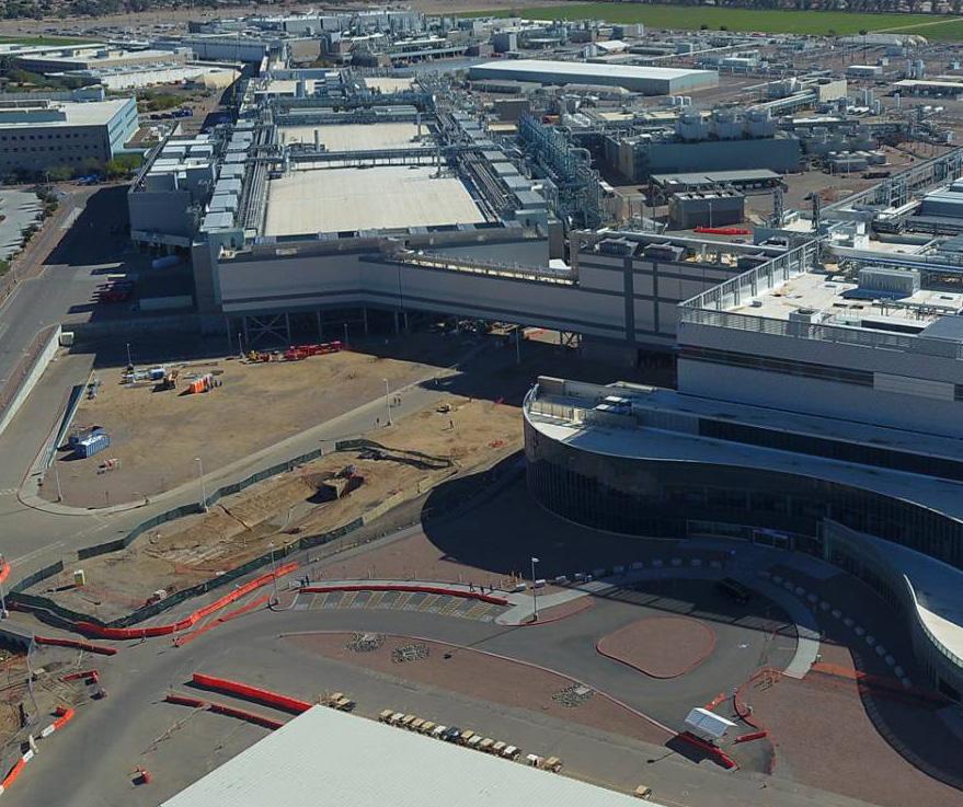
Ocotillo, Arizona
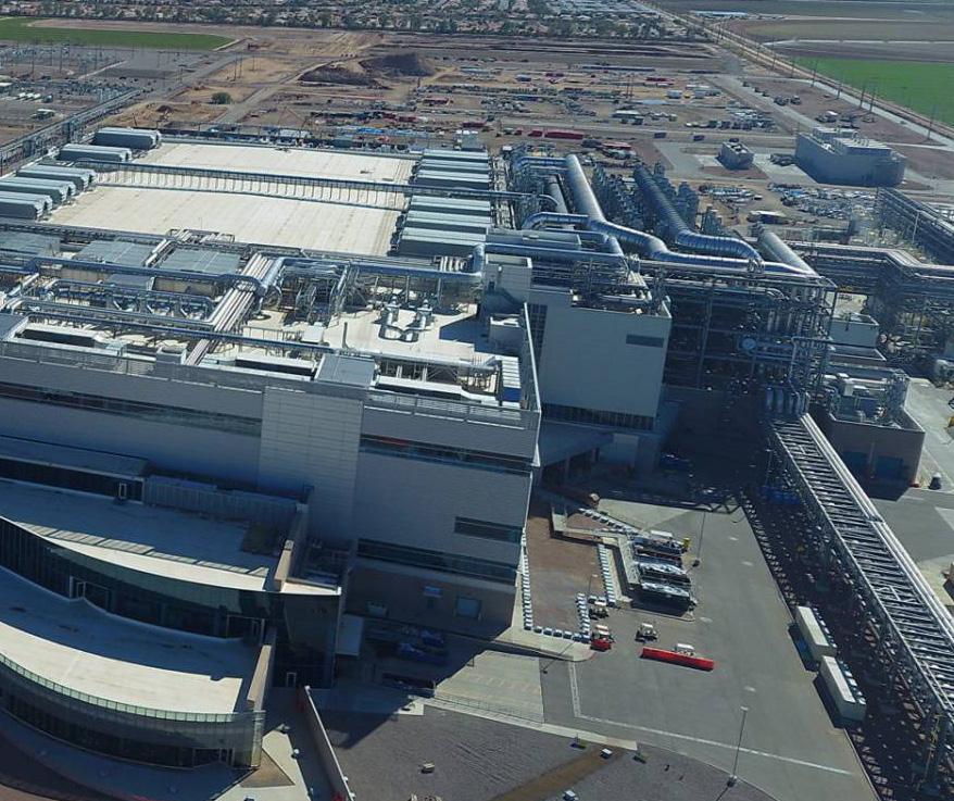
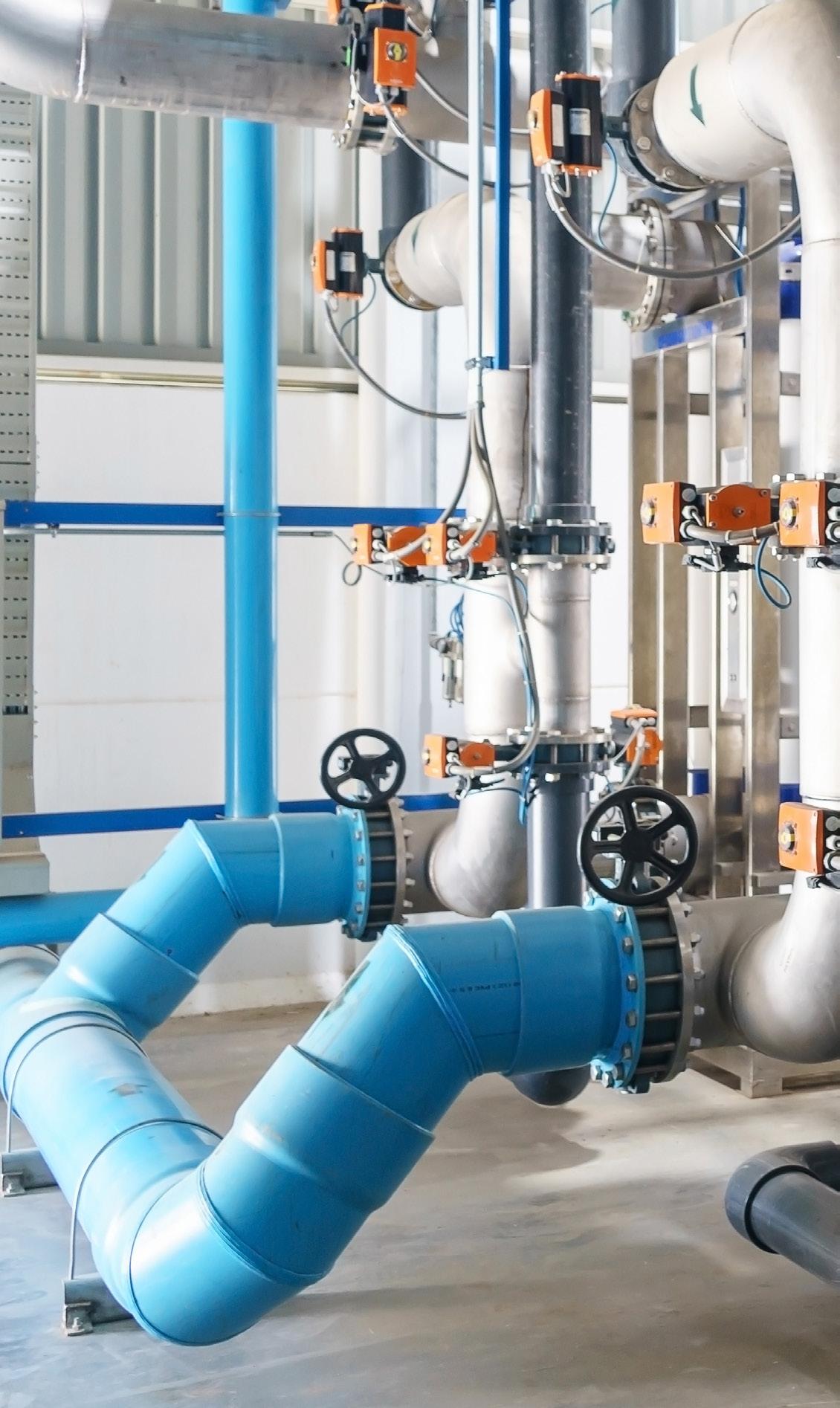
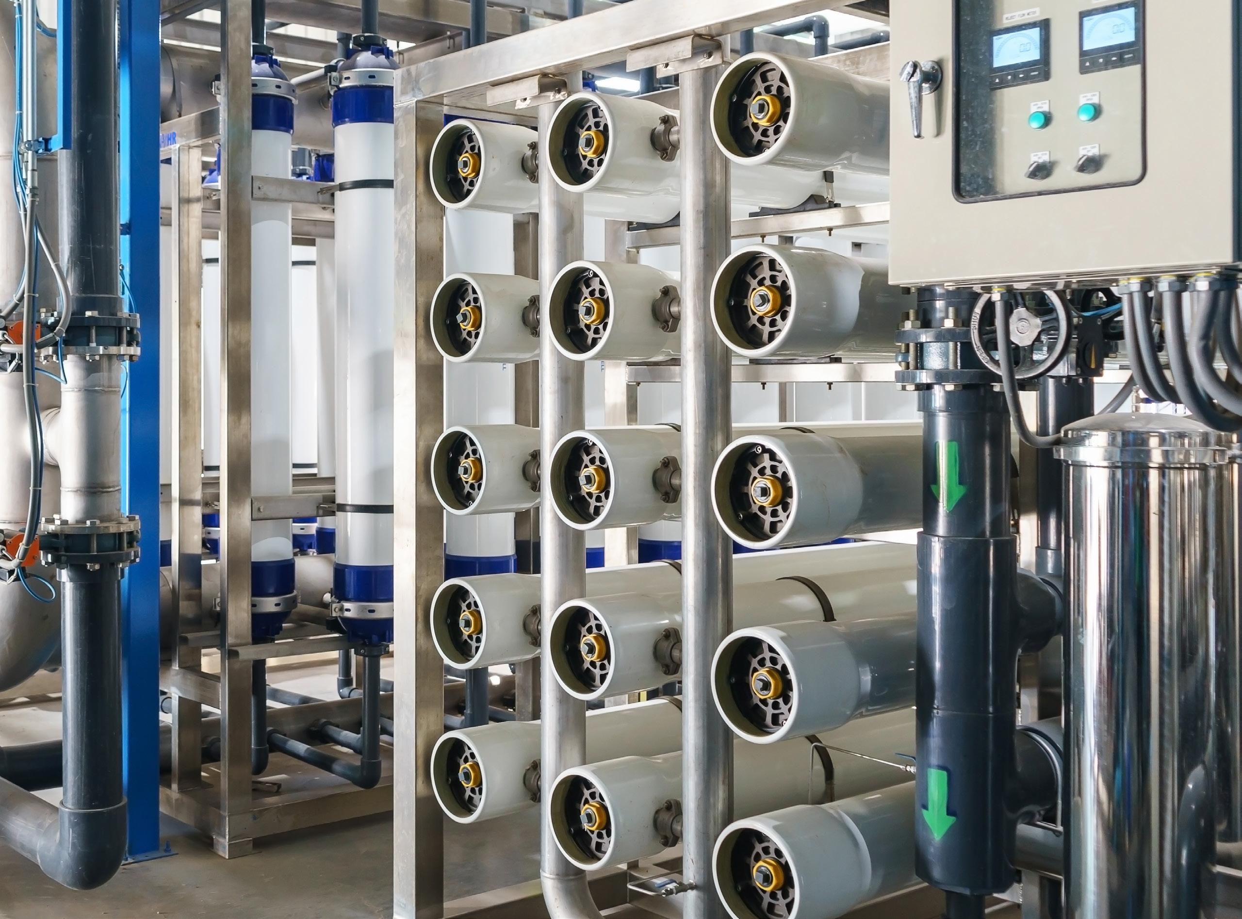
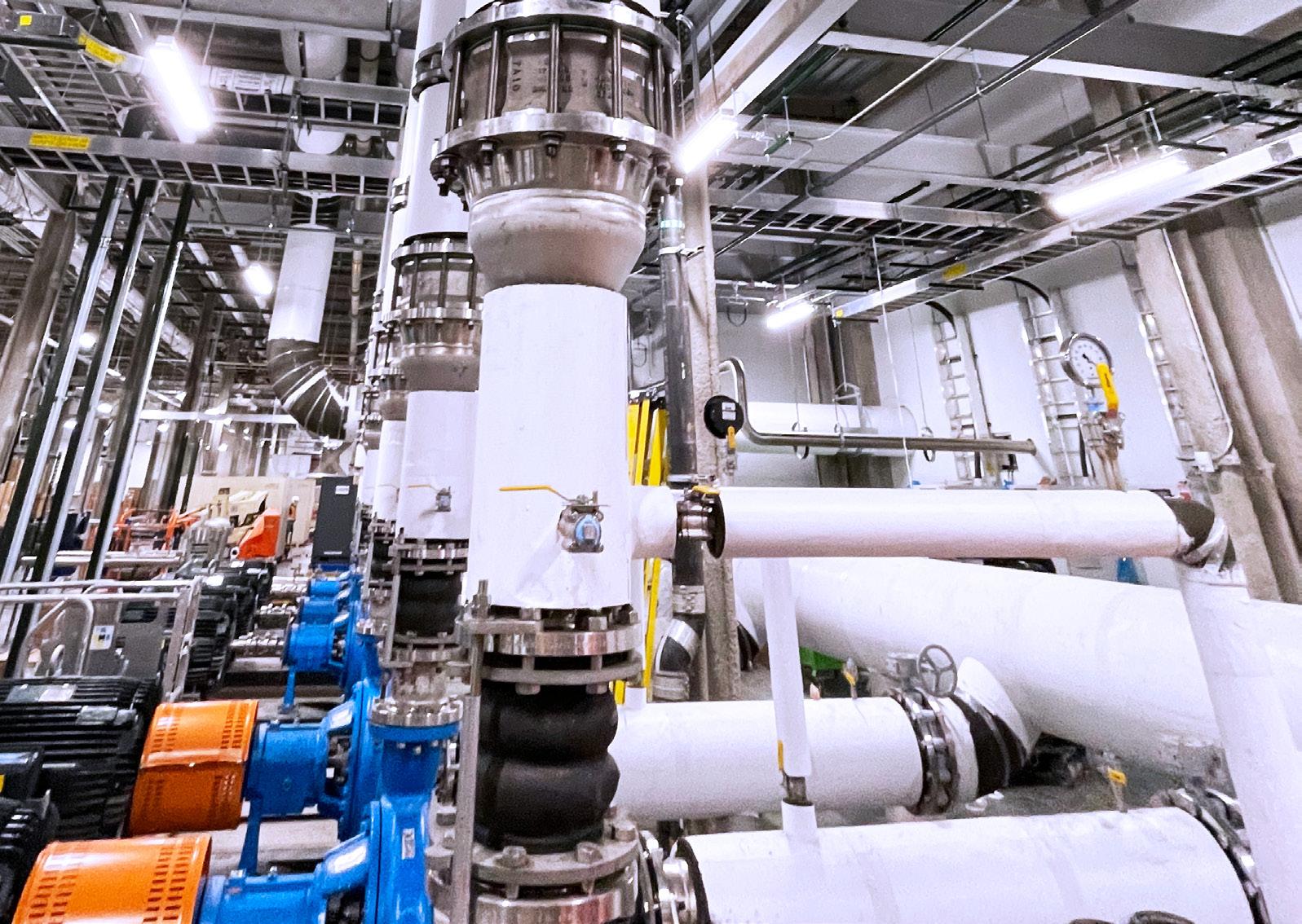
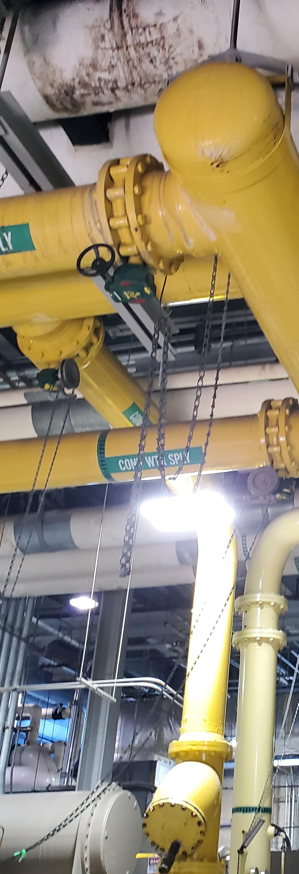
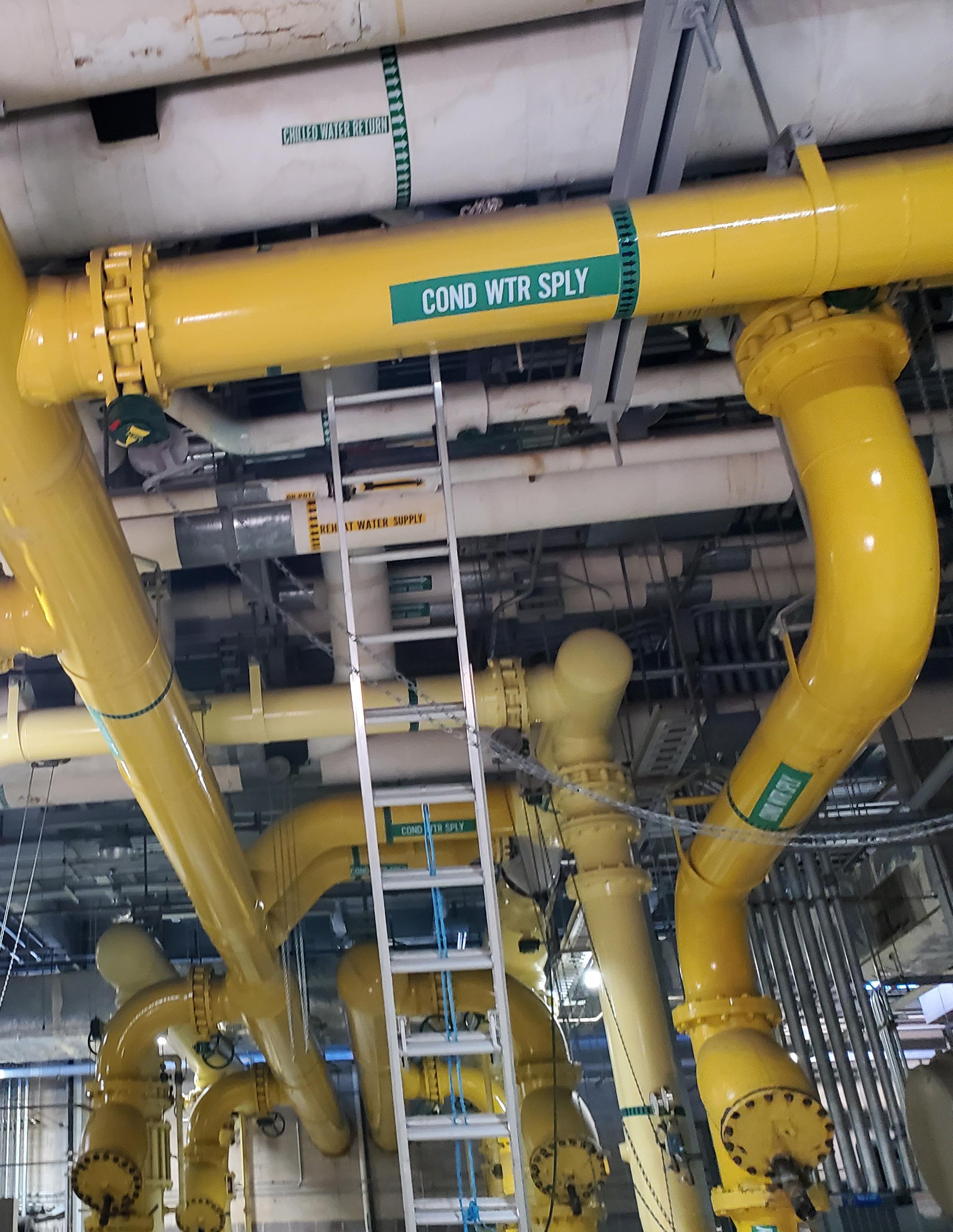
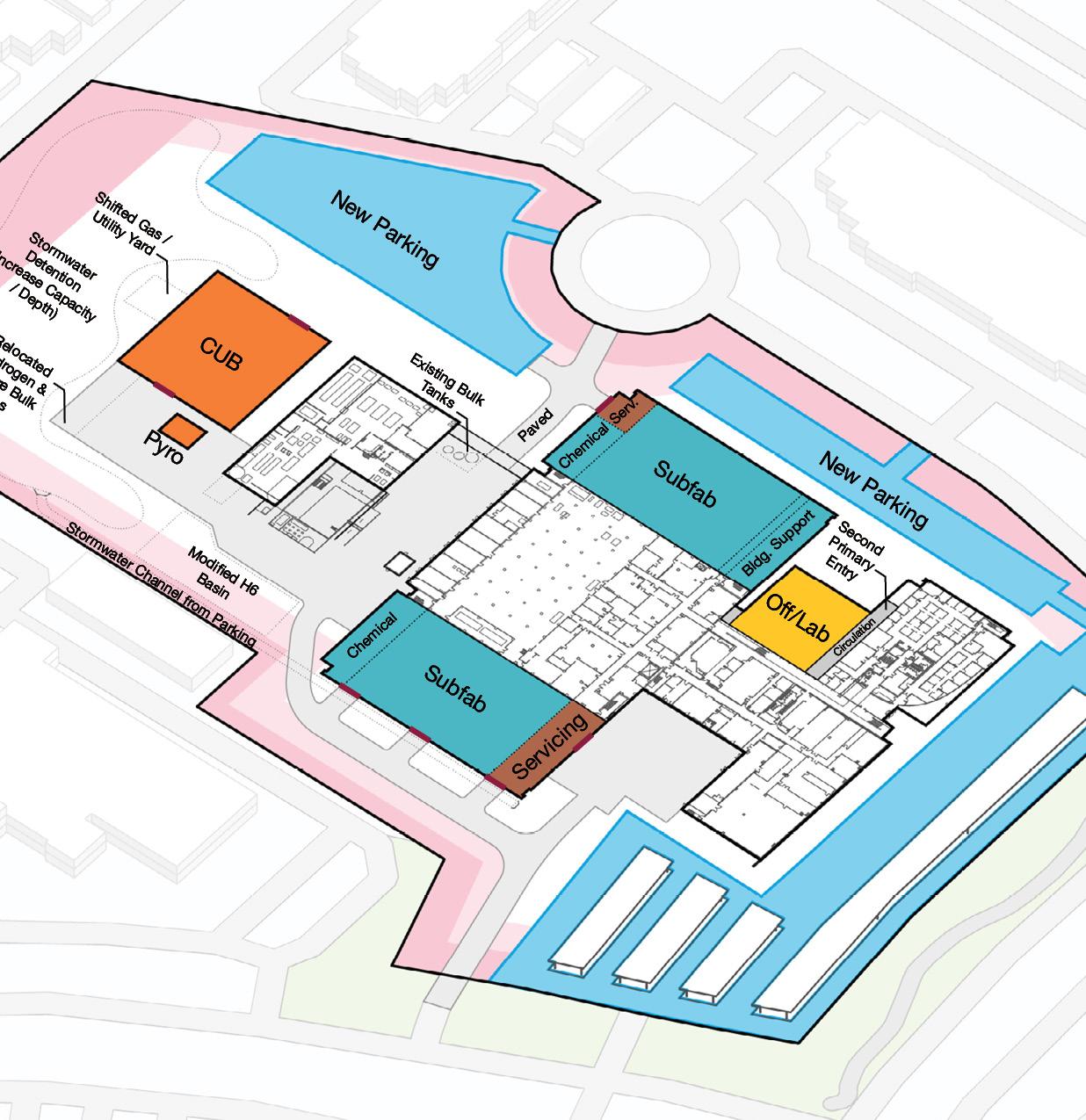
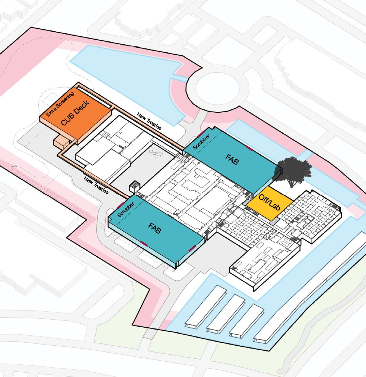
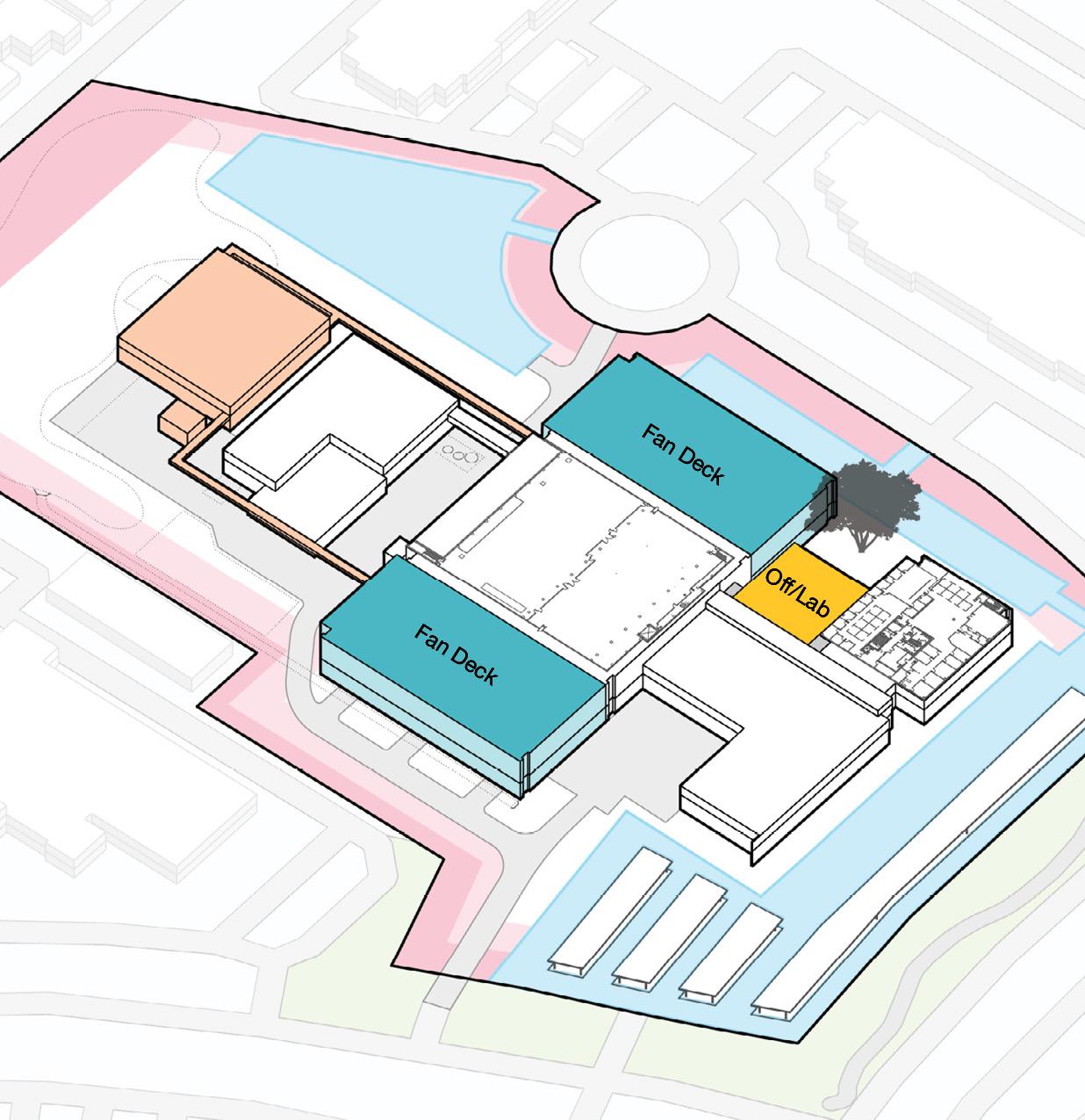
At the Ocotillo campus, Page has been a key partner in delivering architectural and engineering solutions through a design-build contract. Our work spans multiple upgrades, repairs, and alterations across the site, ensuring that existing facilities evolve to meet the demands of leading-edge semiconductor manufacturing. Executed in phases, these renovations integrate architectural, structural, and engineering disciplines to enhance operational efficiency. Notable projects at the campus include the MIT Data Center and PUB Expansion.
Gas/Chemical Layout and Facilitation – Managed project design and engineering for an $8M gas and chemical utility layout, optimizing equipment placement to align with process needs.
Facility Upgrade Services – Upgraded nitrogen, oxygen, and helium systems, along with ultrapure and cooling water infrastructure, to support advanced manufacturing. Expanded process recovery systems to increase capacity.
UPS Power Upgrade – Enhanced power reliability at two primary factories by installing additional UPS systems, achieving 100% redundancy.
Business Continuity Upgrades – Enhanced facility data reliability through design of a new backup data center.
Comprehensive Facility Upgrades – Delivered $24M in site-wide improvements, including process vacuum system validation, ultra-pure water capacity expansion, and highpurity gas distribution enhancements.
Confidential Advanced Packaging Facility
We provide comprehensive start-to-finish design services that include Gap Analysis, Positioning, Programming, Schematic Design, Detailed Design, Construction Documents, and Construction Administration for the retrofit, renovation, and conversion of three existing factories on this site. This scope of work encompassed a total of eight buildings, seven of which contained cleanrooms.
One of the factories underwent a complete retrofit, renovation, conversion, and expansion of a previously mothballed facility. This included an attached support building, an office building, and an expansion to accommodate the clean vestibule, airlock, and loading dock for the Die Sort cleanroom.
The state-of-the-art upgrades to the factories were aimed at enhancing operations for the manufacturing of advanced semiconductor packaging technologies, including the revolutionary 3D packaging technology known as “Foveros.” These upgrades supported new process tools with 14nm (1227) Passive Interposer, TSV Reveal, and C4 technologies, as well as Advanced Wafer Prep, Wafer Level Assembly, HOP Sort, Wafer Sort, Die Sort, Die Prep, Die Storage, and WLA Labs. Additionally, they ensured the ongoing operation of 32nm (1268) generation tools and Optane technology across four buildings of the two existing factories.
Services Provided Architecture of Record / Partial Process Engineering / Construction Administration / Construction Documents / Programming - Positioning - Gap Analysis
Relevancies
Fab / Cleanroom / Central Utility Building (CUB)
Texas
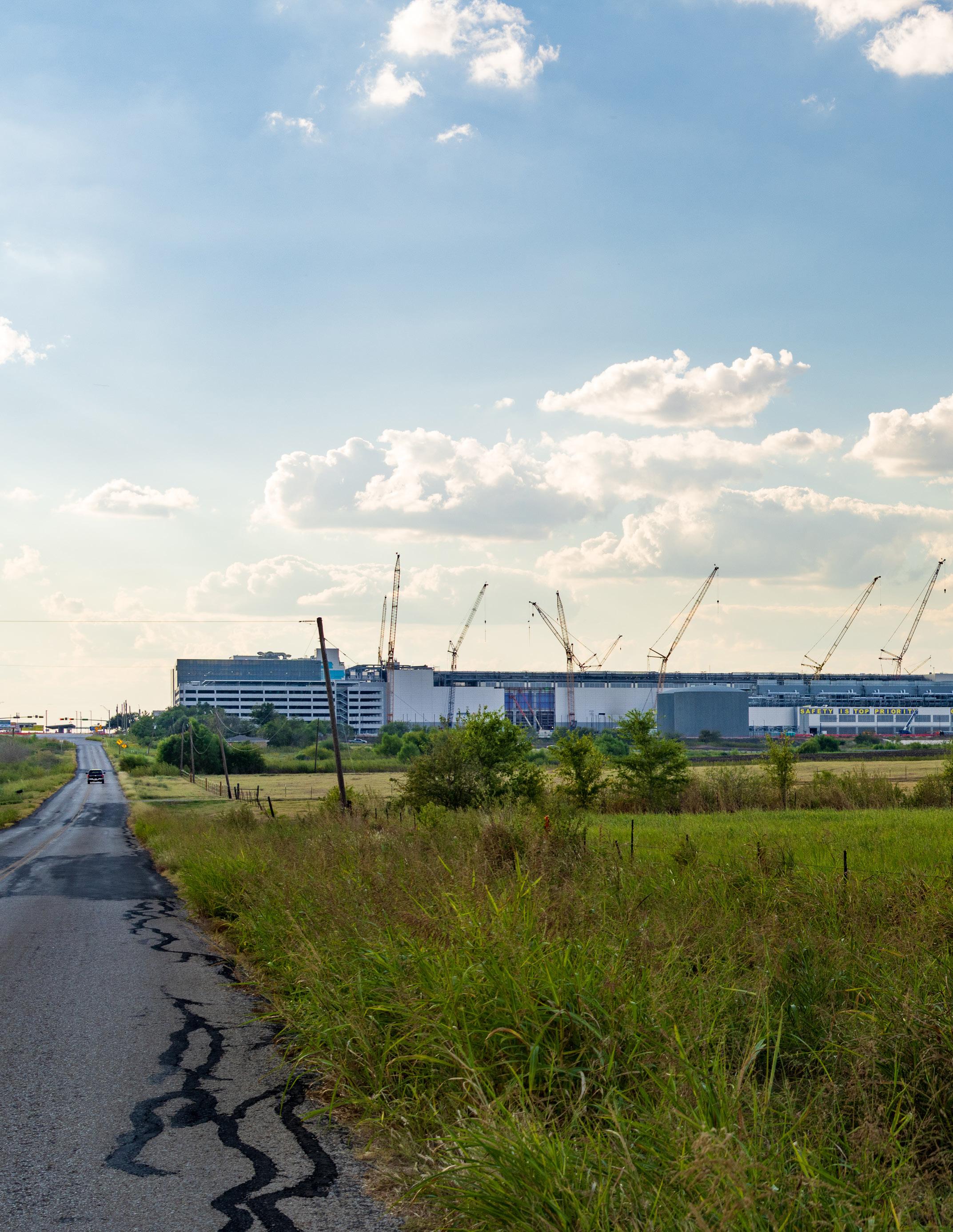
Confidential Semiconductor Manufacturer SM1
Page is providing architectural and engineering design for a next-generation semiconductor manufacturing complex on a 450-acre greenfield site in Sherman, Texas. The development includes four 300mm fabrication buildings, each 1.1 million square feet, featuring 400,000-square-foot cleanrooms, dedicated utility plants, and wastewater treatment systems. A central support building connects the FABs , optimizing workflow, while a separate office building provides space for 1,500 technicians, operators, and engineers, complete with dining, fitness, and recreation areas.
Designed for resilience, all buildings incorporate F3 tornadoresistant elements, on-site water storage, emergency power, fuel reserves, and shelter-in-place zones. The site includes a 1,500-space parking garage, a specialty gas facility, and dual power feeders from Oncor’s high-voltage grid.
Page’s full engineering and design services support a 10-year master plan, ensuring seamlessly phased implementation of all four FABs to drive long-term semiconductor manufacturing growth.
Services Provided
Master Planning / Architecture / MEP Engineering / Process Engineering / Structural Engineering / Interiors / Sustainability / Branding / Urban Design
Relevancies
Fab / CUP / Admin Building / Parking Garage / Cleanroom / VOC / Metrology Lab / Specialty Chemicals / Bulk Gas
Size
1,100,000 SF
Boise, Idaho
Confidential Semiconductor Manufacturer Building
39 Central Utility Plant (CUP)
& Building 51X
At this Boise site, leading-edge infrastructure is the foundation for operational excellence and the expansion of highperformance semiconductor facilities. The Building 39 Central Utility Plant (CUP) & Building 51X projects exemplify strategic advancements that enhance efficiency, sustainability, and scalability—optimizing today’s operations while future-proofing for tomorrow’s breakthroughs.
Since the early 2000s, our longstanding partnership with this Confidential Semiconductor Manufacturer has been instrumental in driving continuous innovation and maintaining industry leadership. Through forward-thinking infrastructure solutions, we have built a resilient, adaptable utility framework that supports sustained growth and meets the evolving demands of semiconductor manufacturing. These investments reinforce a commitment to scalability, reliability, and the next generation of semiconductor excellence.
Services Provided Architecture / Mechanical Engineering / Electrical Engineering / Process Engineering / Fire Protection
Relevancies
Cleanroom / VOC / Space Management / Central Utility Plant (CUP) / Trestle / Water-Wastewater Treatment
Size
4,811,500 SF New Construction, Multi-Phased
Services Provided
Project Management / Architecture / Process Engineering / Mechanical Engineering / Electrical Engineering / Code Analysis / Structural Engineering / Civil Engineering / Landscape / Telecommunications / Fire Protection / Plumbing Engineering / Branding & Graphics / Building Performance Analysis / Commissioning / Interior Design / Lab Planning / Planning / Urban Design / Strategies & Analytics
Relevancies
Fab / GCS / Cleanroom / Metrology Lab / Wastewater Treatment / Warehouse / Chemical Storage / Emergency Response / Hazardous Waste / Specialty Chemical / Bulk Gas / Gas Yard / Hydrogen Chloride (HCl) / Silane (SiH4) / Utility Bridge / Control Building
Gas, Chemical & Slurry (GCS) Systems
As part of the Gas, Chemical & Slurry (GCS) Systems scope, Page developed storage and distribution systems for a new greenfield fabrication facility. This involved the precise design of specialty gas and process chemical handling, including waste chemical management. Page provided extensive technical services such as chemical classification, equipment layout, utility hookup design, system sizing calculations, and advanced modeling for piping flow and stress analysis. These elements were critical in securing necessary permits and ensuring smooth construction execution.
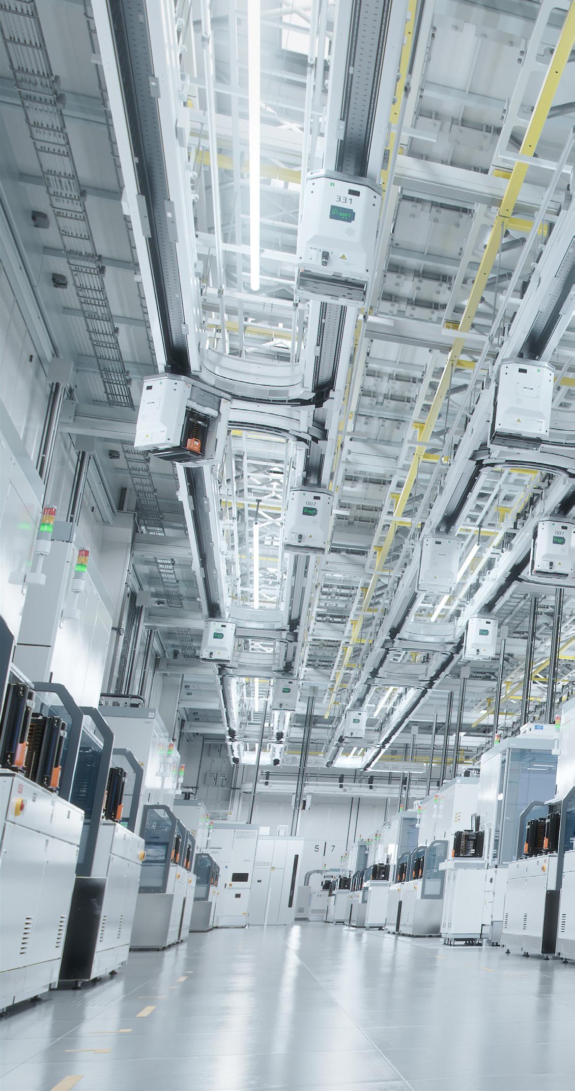
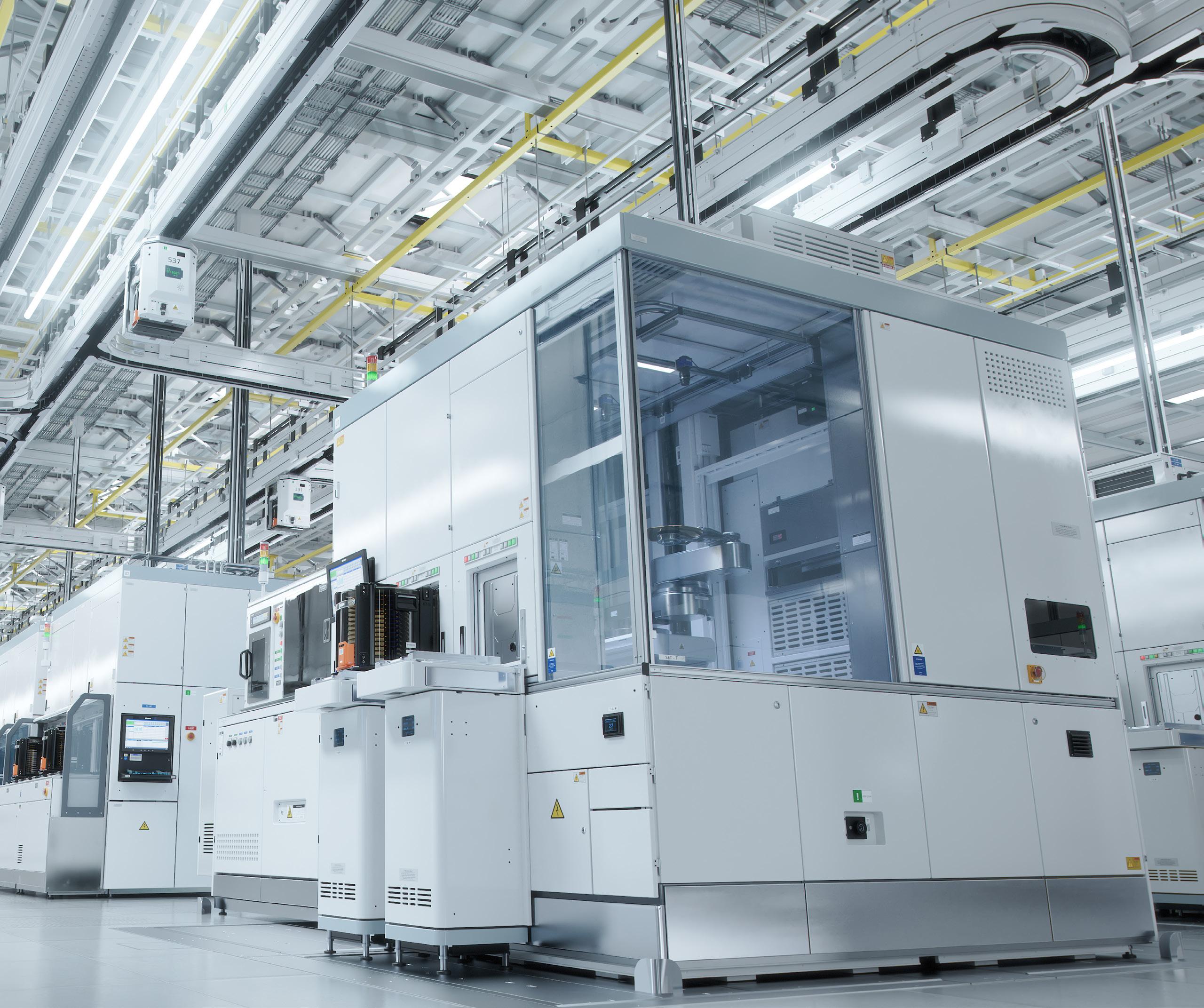
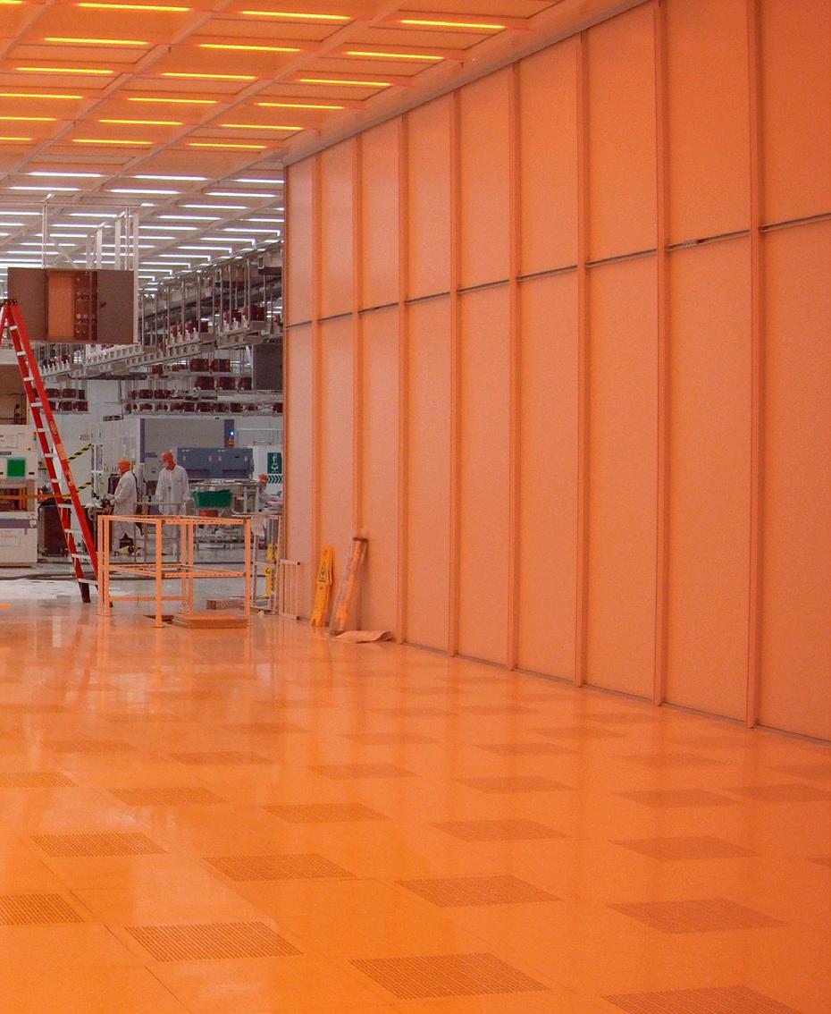
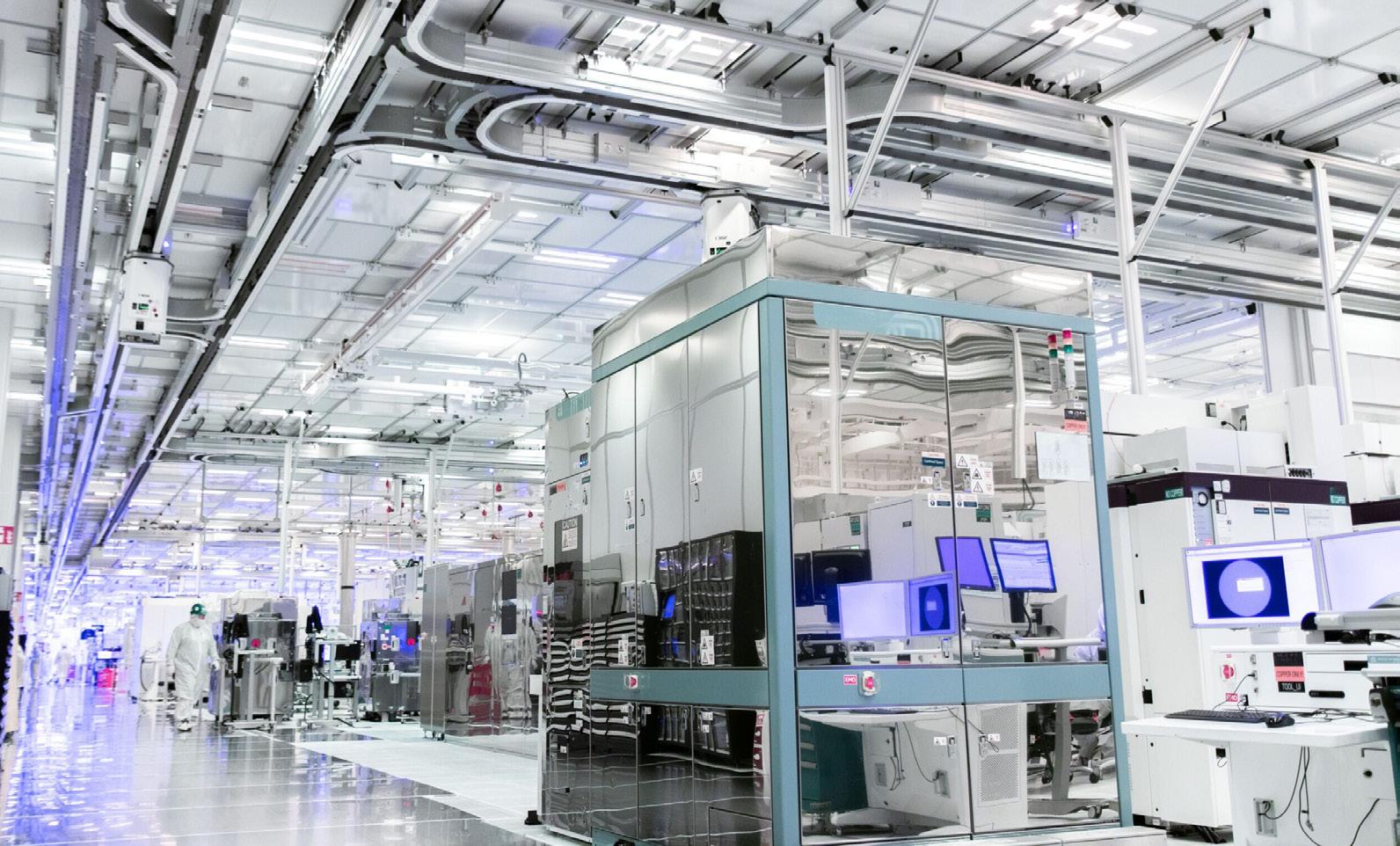
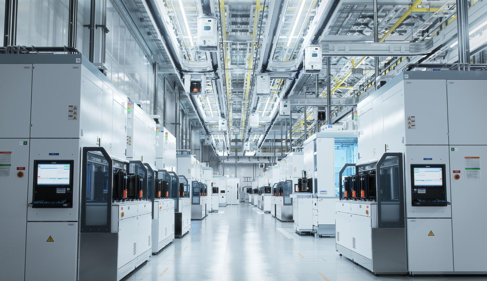
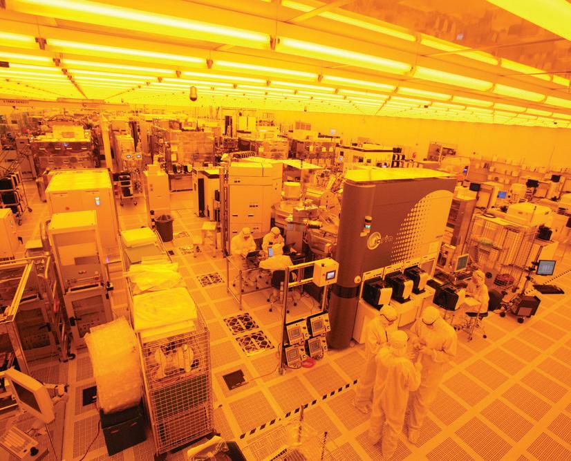
Cleanroom
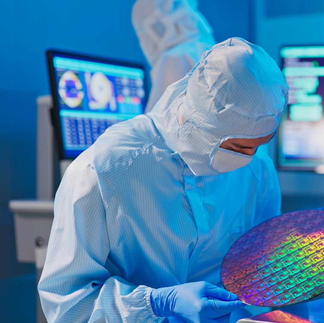
FAB1 boasts 1.2 million square feet of class-1 cleanrooms, including Fabrication and Sub FAB areas. As engineer of record, Page led architecture, structure, mechanical, process, electrical, and I&C work. We provided engineering analysis, managed permitting, attended client meetings, and oversaw construction. The cleanroom package included 3,000+ construction drawings.
Warehouses
Beyond the fabrication infrastructure, Page led the development of warehouse facilities, comprising eight buildings with a total footprint of 280,000 square feet. These warehouses serve vital functions, including secure chemical storage, emergency response, hardware innovation, waste segregation, and hazardous waste management. The Hardware Innovation Center provides space for research and prototyping, while the Wafer Granulator supports production efficiency. To enhance overall site functionality, Page provided civil and landscape design, electrical and mechanical engineering, fire protection planning, and permitting services.
Designed for efficiency and safety, the facility integrates a Chemical Warehouse for secure storage, an Emergency Response Center for rapid incident management, and a Hardware Innovation Center for R&D and prototyping. Waste Segregation and Hazardous Waste facilities ensure responsible byproduct handling, while a Wafer Granulator, Gate House, and Guard Shack enhance security and operations.
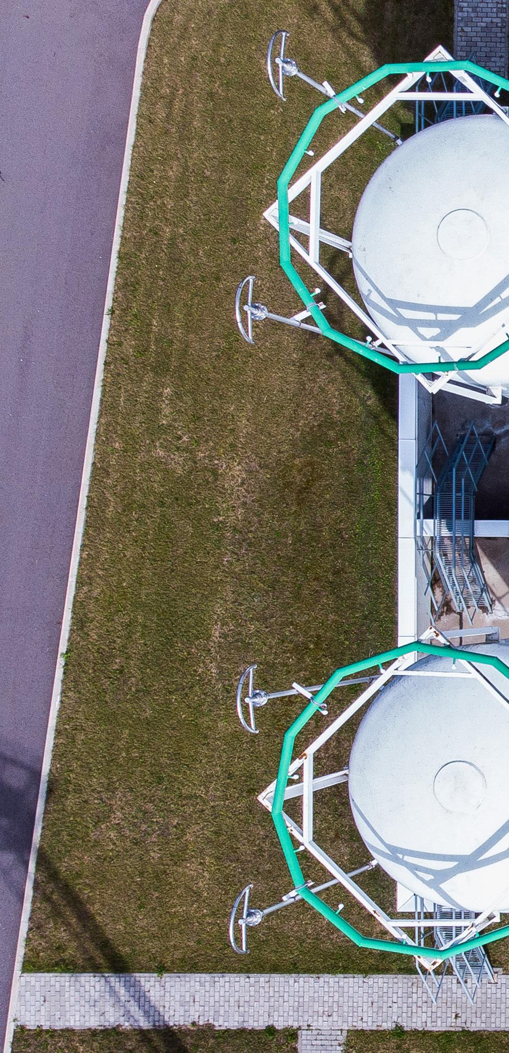
Bulk specialty gas (BSGS) & ISO Yard
The Bulk Specialty Gas (BSGS) & ISO Yard was developed as a turn-key project within a broader campus initiative to support semiconductor production. This facility enables the manufacturing of advanced logic chips used in high-performance computing, 5G, and artificial intelligence applications.
Key features include:
Integrated Control Buildings: three dedicated buildings for real-time monitoring and management.
Specialized ISO Canopies: six canopies designed for safe handling of H2/N2, SiH4, NH3, He, N2O, and NF3 gases.
Dedicated HCl and CO2 Facilities: HCl ISO building and CO2 tank with supporting equipment pad.
Grade-Supported Equipment Pads: stable foundation ensuring safety and operational integrity.
Multi-Level Utility Bridge: Optimizing connectivity across facility infrastructure.
Research & Development
Albany, New York
NY CREATES Albany NanoTech Complex
NY CREATES is the owner and operator of the Albany NanoTech Complex, the nation’s largest and most advanced non-profit semiconductor R&D facility. As a leading-edge hub for innovation, Albany NanoTech brings together industry leaders, academic institutions, and international partners to drive the development of next-generation chips and fabrication processes.
For more than two decades, this state-of-the-art complex has been at the forefront of groundbreaking advancements in semiconductor technology. Today, it continues to expand its global partnerships, attracting industry pioneers in the semiconductor market, energy efficiency and renewable energy technologies.
Page has played a pivotal role in shaping this visionary complex—contributing to the master plan and designing many of its advanced research facilities.
Services Provided
Programming / Master Planning / Architecture / Project Management / Engineering / Telecom / Security / Graphics / Sustainability
Relevancies
Research & Development (R&D) / Tools / Cleanroom / Specialty Chemical / Bulk Gas / Metrology Lab / Data Center
Pioneering the Future of Semiconductor Innovation
To support the Albany NanoTech Complex’s rapid growth, NY CREATES developed a Master Plan to guide its expansion. As the anchor of New York State’s Tech Valley, the Complex has become a global hub for semiconductor innovation, attracting 300+ industry and government partners with its world-class facilities and cutting-edge technology.
The master plan provided a strategic framework for three major phases of expansion, adding over 1 million square feet of state-of-the-art research and development space—more than doubling the size of the Complex.
Phase 1: NanoFab Xtension (NFX) – A significant expansion of cleanroom and R&D facilities.
Phase 2: Zero-Energy Mixed-Use Facility (ZEN) – A highperformance, energy-efficient research and collaboration space.
Phase 3: NanoFab Reflection – A current expansion aimed at enhancing advanced semiconductor research capabilities.
NanoFab Xtension (NFX): Advancing Semiconductor Innovation
The NanoFab Xtension (NFX) Building stands as a symbol of the power and promise of emerging technologies. As part of NY CREATES, a world leader in nanoscience R&D and education, NFX houses more than 120 wafer processing and inline metrology tools, supporting the development of next-generation semiconductor manufacturing.
Class 1,000 cleanrooms enable leading-edge research and production of the most advanced chip manufacturing tools. Specialized structural features support heavy manufacturing equipment and mitigate vibrations. The facility also hosts 300mm advanced lithography platforms, including 193nm immersion and EUV lithography, along with technologies for planarization, copper plating, etch development, ion implantation, thin film deposition, and wet cleaning.
NFX is a 500,000-square-foot facility, featuring 55,131 square feet of cleanrooms, solidifying its role as a cornerstone of semiconductor research and innovation.
Zero Energy Nanotechnology Building (ZEN)
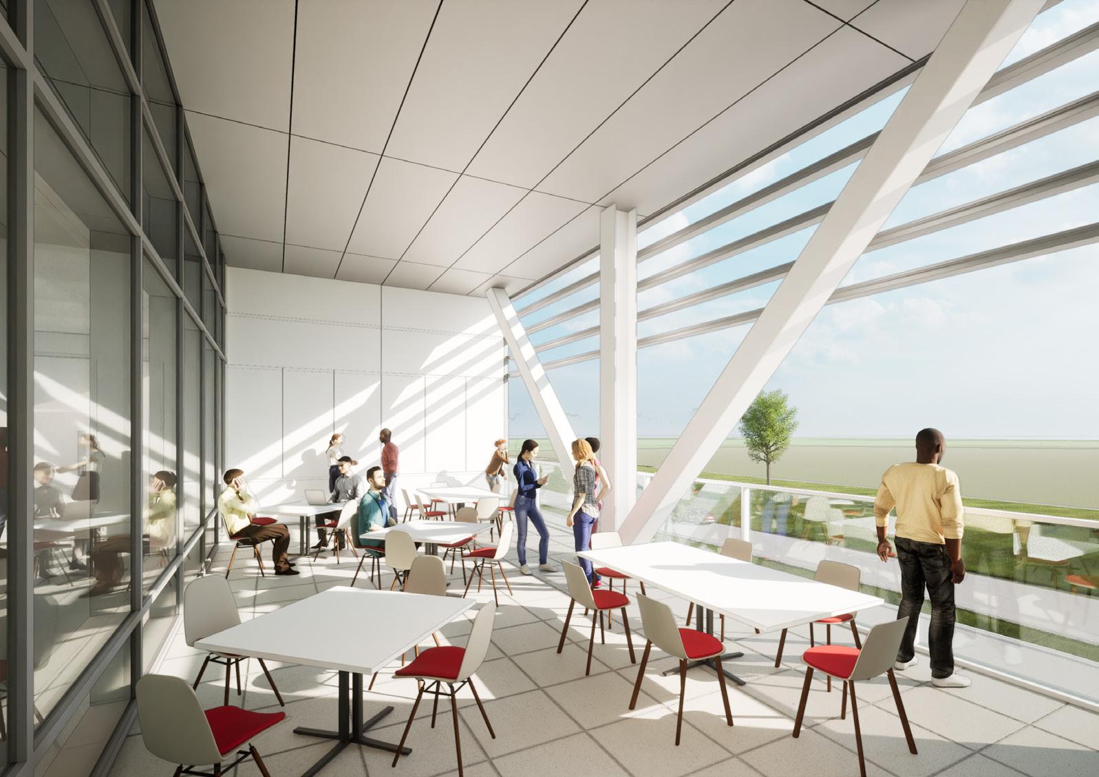
The Zero Energy Nanotechnology (ZEN) Building is a groundbreaking 363,000-square-foot mixed-use facility— the largest zero-energy-capable building of its kind in the United States at construction completion. Located within a dynamic research environment that hosts 3,000 scientists, engineers, faculty, students, and staff, ZEN serves as a hub for innovation, industry collaboration, and sustainable design.
The ZEN Building supports a wide range of research, development, and teaching activities. The facility features:
Office space for research partners in business and industry.
Flexible research labs for faculty and students.
A 10,000-square-foot community hub beneath an ultralight ETFE roof system, designed for formal and informal collaboration.
ZEN serves as a living laboratory for clean and renewable energy technologies, reinforcing NY CREATES' leadership in high-tech research and sustainability. The NYS ITS Tier 3 Data Center, housed on the first floor, provides critical IT infrastructure for nearly 60 New York State agencies. Through waste heat recovery, the data center prevents temperature buildup while efficiently providing warmth for the rest of the building eliminating need for fossil fuel consumption all year.
By integrating leading-edge design, industry partnerships, and energy-efficient solutions, the ZEN building embodies the extraordinary potential of nanotechnology and sets a new standard for sustainable mixed-use facilities.
Innovative Energy Efficiency Strategies
Working in collaboration with NY CREATES and the New York State Energy Research and Development Authority (NYSERDA), ZEN was designed using advanced energy modeling to optimize efficiency. Ongoing research is using the building as a digital twin to study data-driven energy conservation measures and operational optimizes opportunities.
Sustainability Features
70% Daylight Harvesting
59.4% Solar Power Savings Data Center Heat Recovery Net-Zero Future Generation

University of Texas at Austin Montopolis Research Campus
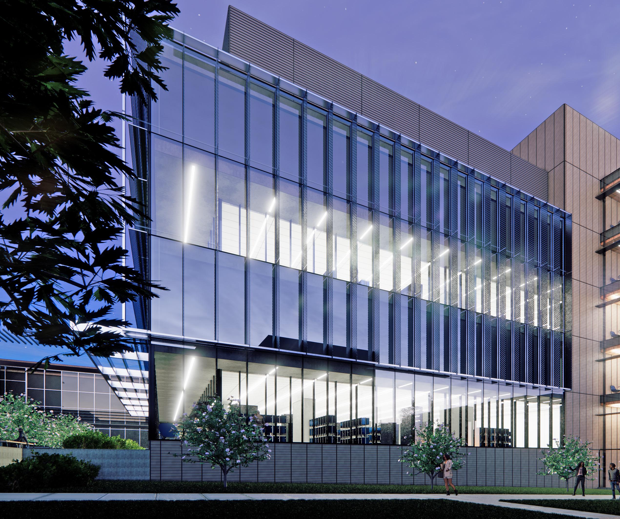
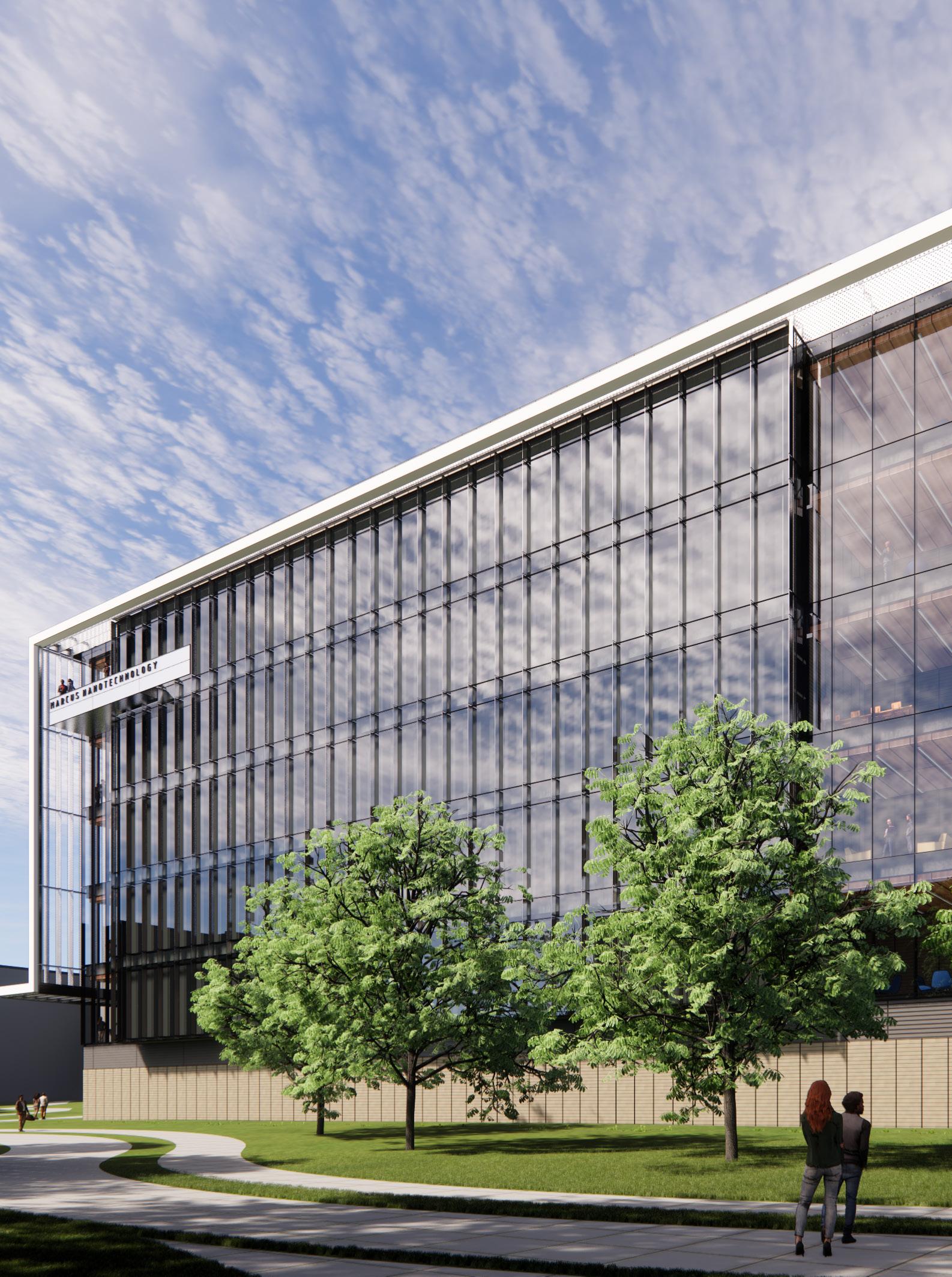
For nearly four decades, the University of Texas at Austin Cockrell School of Engineering and the Texas Institute for Electronics (TIE) Montopolis Research Center have been at the forefront of industry collaboration, hosting leading partners such as Sematech. Today, the historic facility is evolving to meet the demands of next-generation semiconductor research and production.
Page’s cleanroom renovation pushes performance to new heights, transforming existing fabrication spaces into ISO 4 (Class 10) and ISO 5 (Class 100) environments. With a focus on process optimization, key infrastructure upgrades include Acid Waste Neutralization, Hydrogen Fluoride Waste Treatment, Ultra-Pure Water production, Gas and Chemical Distribution, Supervisory Control and Data Acquisition (SCADA), and Toxic Gas Monitoring Systems (TGMS), Building Automation System (BAS), Clean Air Handling, and HVAC. These enhancements create a world-class research ecosystem designed for flexibility, scalability, and seamless took transitions.
This state-of-the-art fabrication facility—known as the Fab— will serve as a vital hub for the Texas Institute for Electronics (TIE), a powerhouse public-private partnership uniting the State of Texas, top semiconductor and defense electronics firms, national labs, and 13 academic institutions. This initiative restores leading-edge semiconductor manufacturing to U.S. soil, strengthens the supply chain, safeguards national security, and cultivates the next generation of industry pioneers.
Purpose-built to accelerate breakthroughs in semiconductor research and development (R&D) and 2.5D/3D semiconductor packaging, the project followed a fast-track delivery process. The reenvisioned Fab is equipped with the critical infrastructure needed to fuel discovery, innovation, and global leadership in advanced electronics.
Services Provided
Project Management / Architecture / Interior Design / Process Engineering / Lab Planning / Fire Protection / Mechanical Engineering / Electrical Engineering
Relevancies
R&D / Cleanroom / Specialty Chemicals / Bulk Gas / Ultrapure Water / SCADA / Toxic Gas Monitoring (TGMS) / Semiconductor Packaging
Size
226,918 SF Renovation
Georgia Tech Institute of Matter & Systems
MicroFUSE Enabling
Services Provided Architecture / Structural Engineering / MEP Engineering / Process Engineering / Construction Management Selection Support
Relevancies
Higher Education / Semiconductor / Research & Development (R&D)
Size
3,400 SF Renovation / Retrofit
Selected through a competitive process, Page is leading the expansion of the Marcus Building’s inorganic cleanroom for the Institute of Matter and Systems. The challenge? A precisiondriven 1,500-square-foot ISO 5 cleanroom fit-out seamlessly integrated with the existing ballroom-style cleanroom through a dedicated Move-In/Move-Out path. With a bay-and-chase configuration designed to optimize laminar flow, the space meets rigorous cleanroom certification standards—despite structural constraints imposed by the contiguous slab.
Page’s design embraces adaptability, ensuring Georgia Tech’s research-driven program can evolve without interruption. A strategic utility delivery system allows for seamless tool reconfigurations, eliminating reliance on external contractors and minimizing downtime.
Playing a critical role in selecting the construction management (CM) team, Page ensured the project is executed with the precision and expertise required for a world-class, high-performance cleanroom environment.
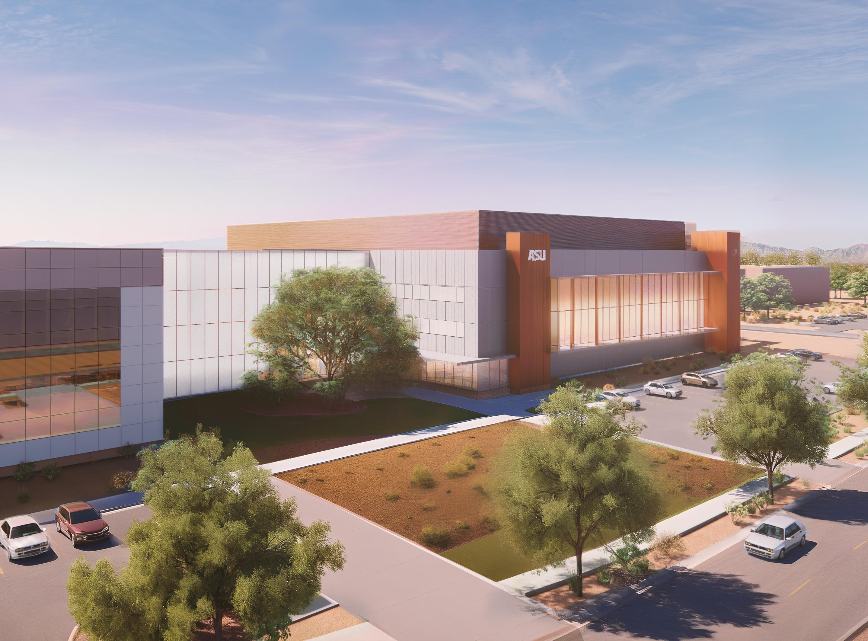
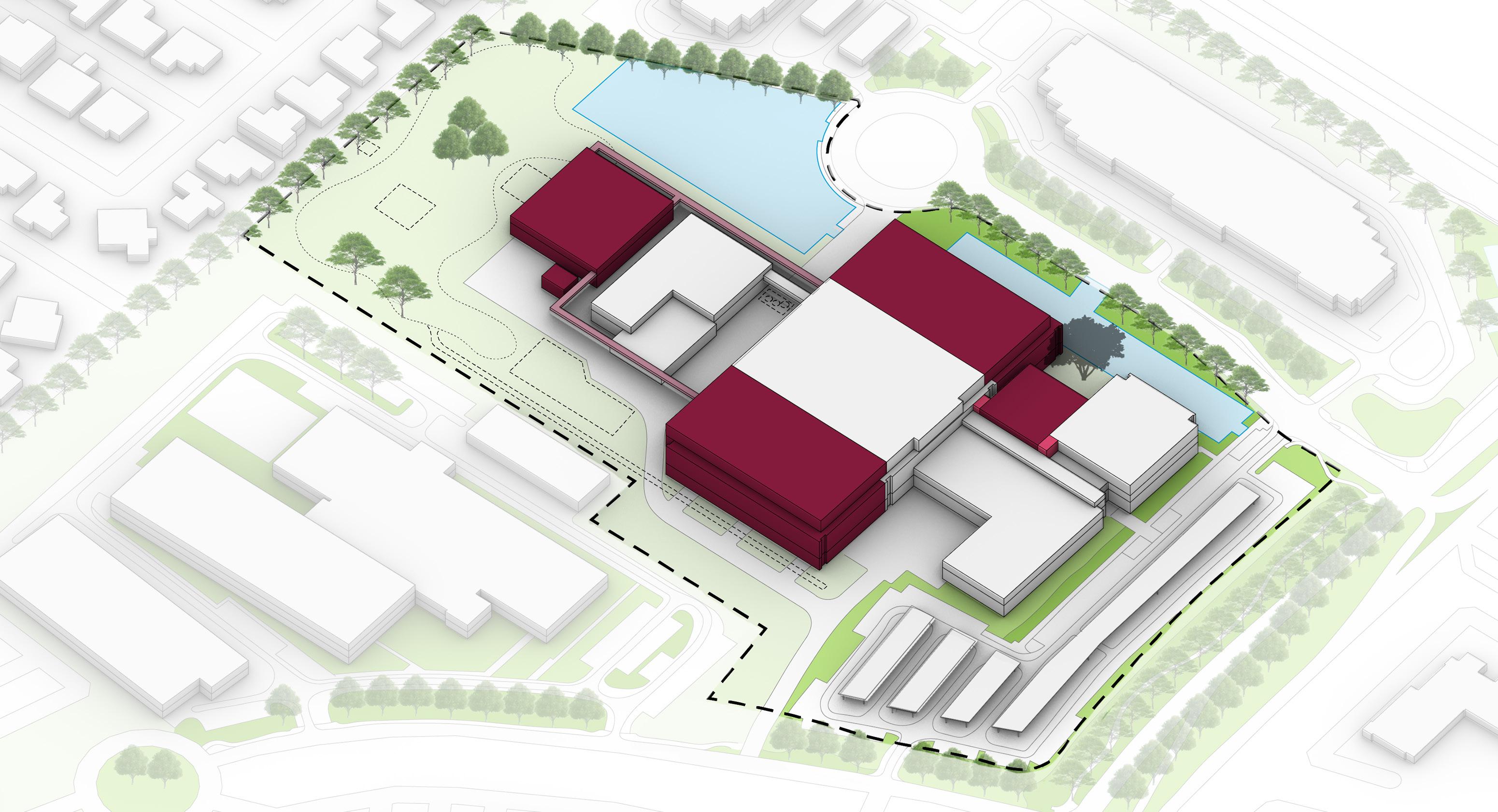
Arizona State University MacroTechnology Works
Originally built in 1997 by Motorola, MacroTechnology Works (MTW) is a 261,188 GSF specialized research and fabrication facility at the center of Arizona State University’s Research Park. Supported by a 26,608 GSF Central Utility Building, the site totals 287,796 GSF. MTW is more than infrastructure; it is a world-class hub that delivers research and fabrication capabilities on a scale unmatched by any other university. It creates direct pathways for ASU to engage industry and drive recruitment, innovation, and national research leadership.
As part of this Facility Master Plan, ASU and the planning team analyzed every aspect of MTW, including infrastructure, users, tools, and active projects, while engaging stakeholders to uncover opportunities to maximize utilization and performance. At the same time, expansion scenarios were tested to push the boundaries of what the site could achieve. The focus was clear: expand fabrication space on the north and south sides of the existing building to maximize cleanroom capacity and reinforce MTW’s role as a singular resource within ASU and beyond.
The result is ambitious. The plan identifies up to 224,400 GSF of new capacity, nearly doubling the site’s total footprint and almost tripling cleanroom space. Designed with flexibility, the expansion can be executed in one bold move or phased strategically over time. Either path positions MTW to scale as a powerful engine for discovery, innovation, and global impact.
Services Provided
Campus Planning / Architecture / Interiors / Engineering / Programming / Lab Planning Assessment / Planning / Infrastructure Planning
Relevancies
Master Planning / Fab / Cleanroom / Central Utility Building / Research & Development (R&D)
Rachel Romero Associate Principal /
Jonathan
Sylvie PhD, PE, PMP, FHR Chief Revenue Officer jsylvie@pagethink.com