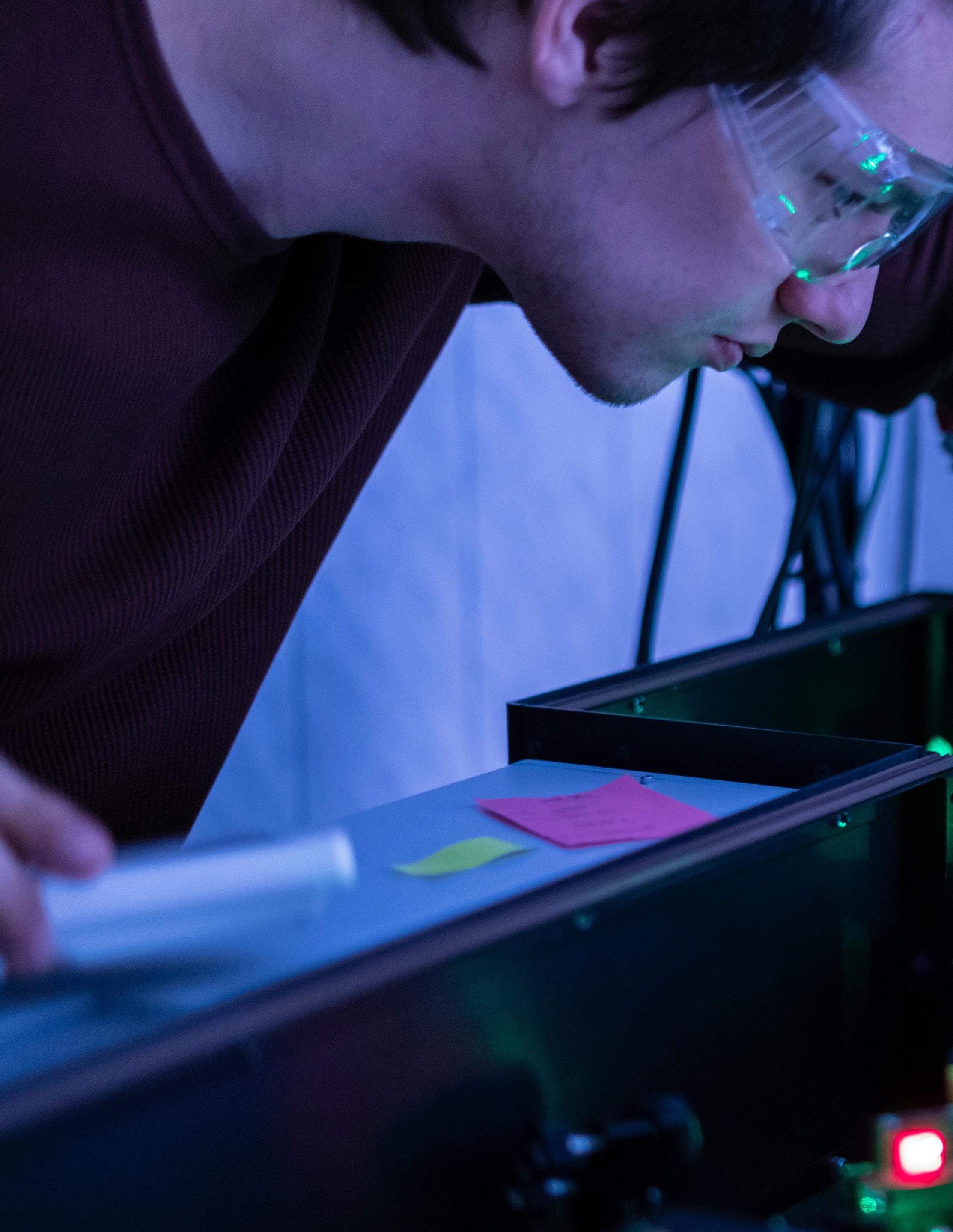
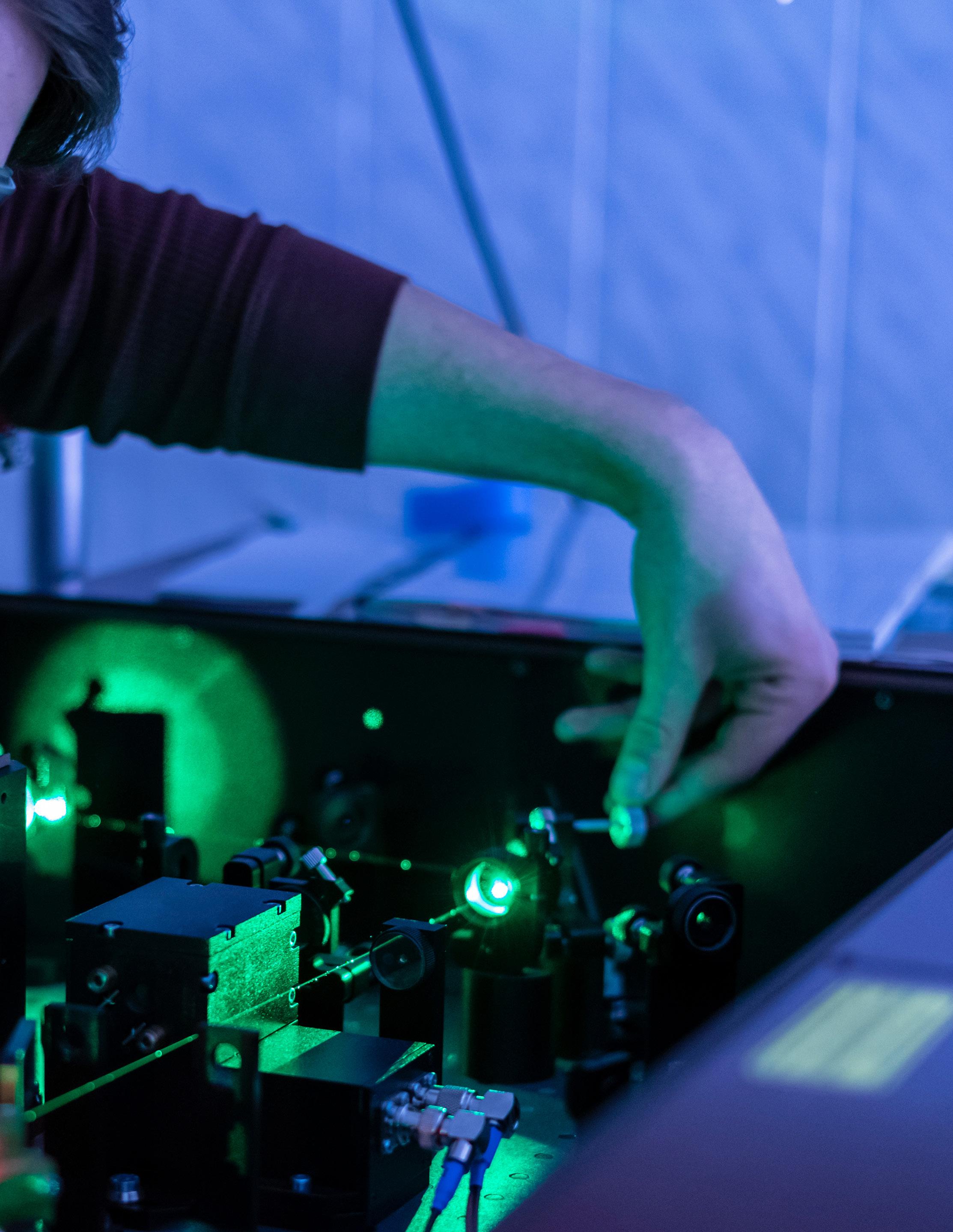
Advanced Manufacturing
Designing tomorrow’s innovations
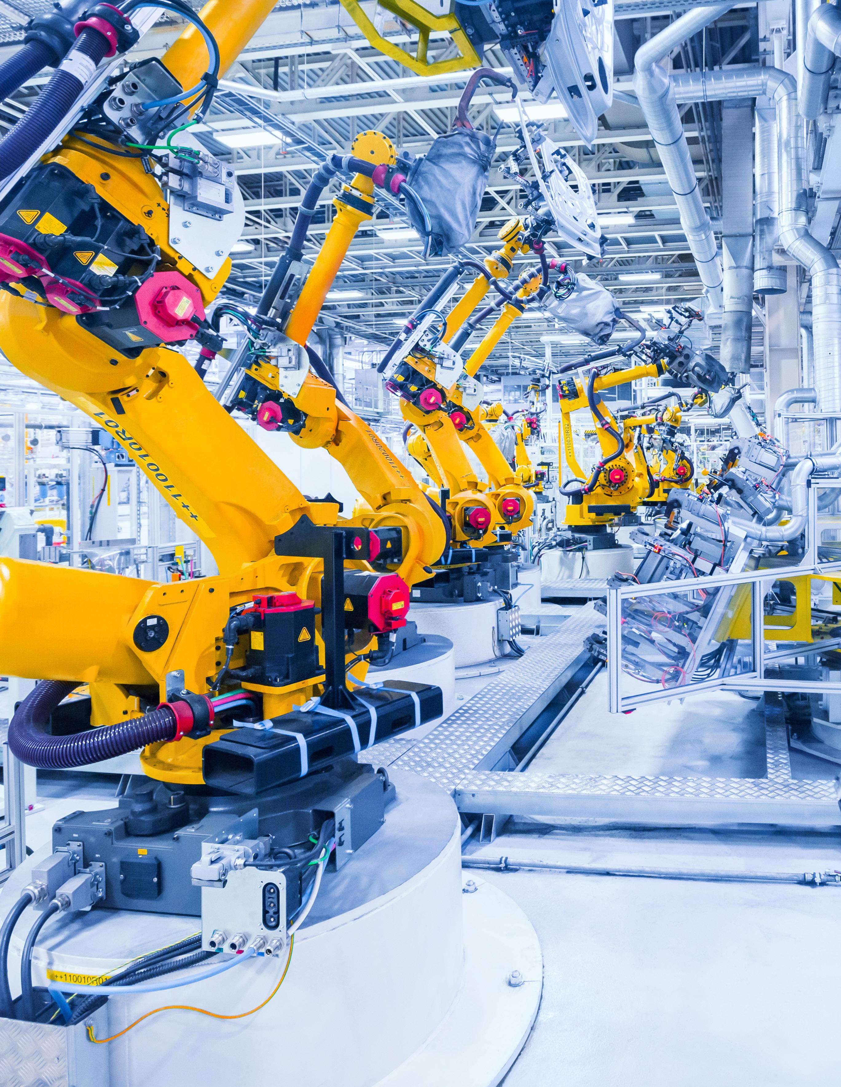
Manufacturing is evolving—driven by automation, data, and engineering breakthroughs. Page, now Stantec partners with industry leaders in semiconductors, electric vehicles, energy storage, and more to design leading-edge facilities, from cleanrooms and tool hookups to process utilities and water/wastewater management.
Ranked among the top 10 in manufacturing and semiconductor facility design, we create solutions that enhance precision, efficiency, and sustainability. Whether shaping lithium battery production, solar advancements, or next-gen automotive manufacturing, our expertise keeps clients ahead of the curve— ensuring facilities perform at the highest level today while remaining adaptable for the future of production, research, and development.
We design and engineer highperformance semiconductor and manufacturing facilities that drive innovation, optimize production, and accelerate time to market for the world’s most advanced industries.
Automotive
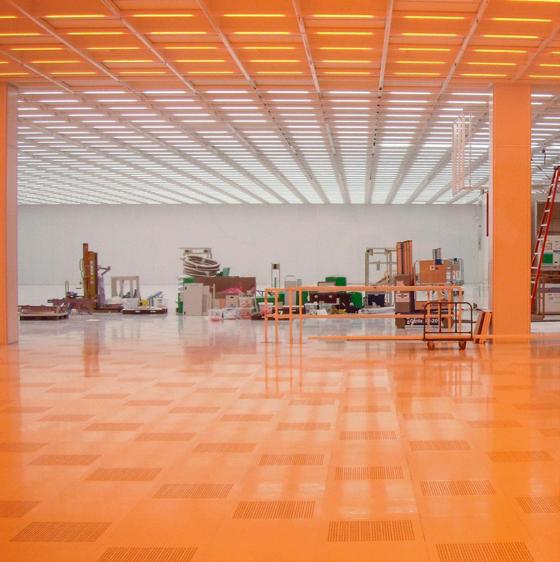
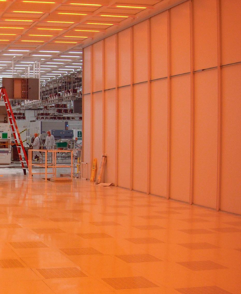
Cleanrooms
Electric Vehicles
Energy Storage
Facility Planning
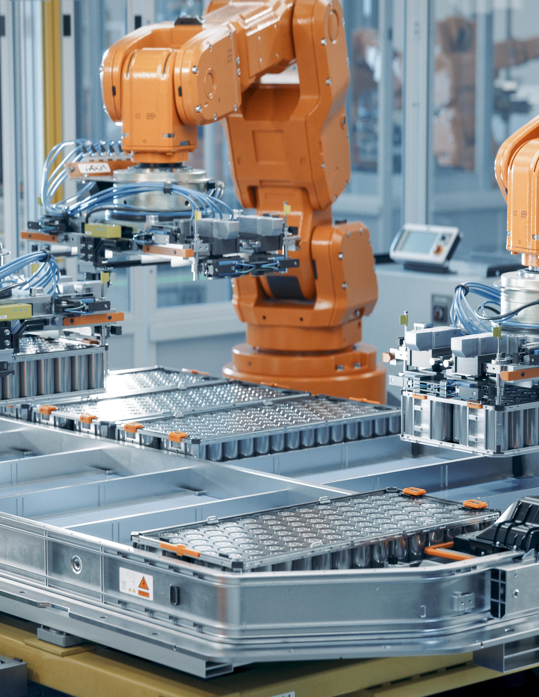
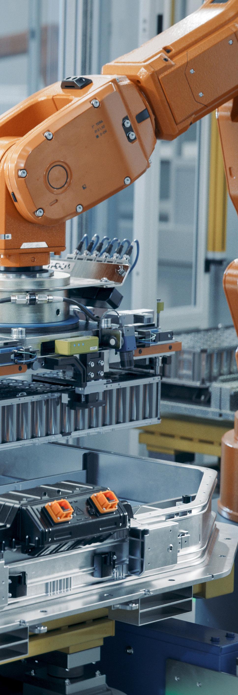
Lithium Battery
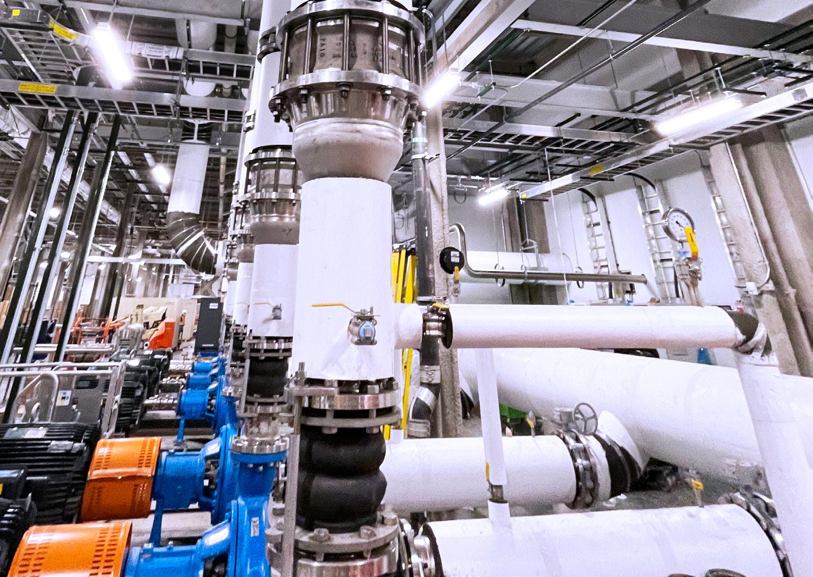
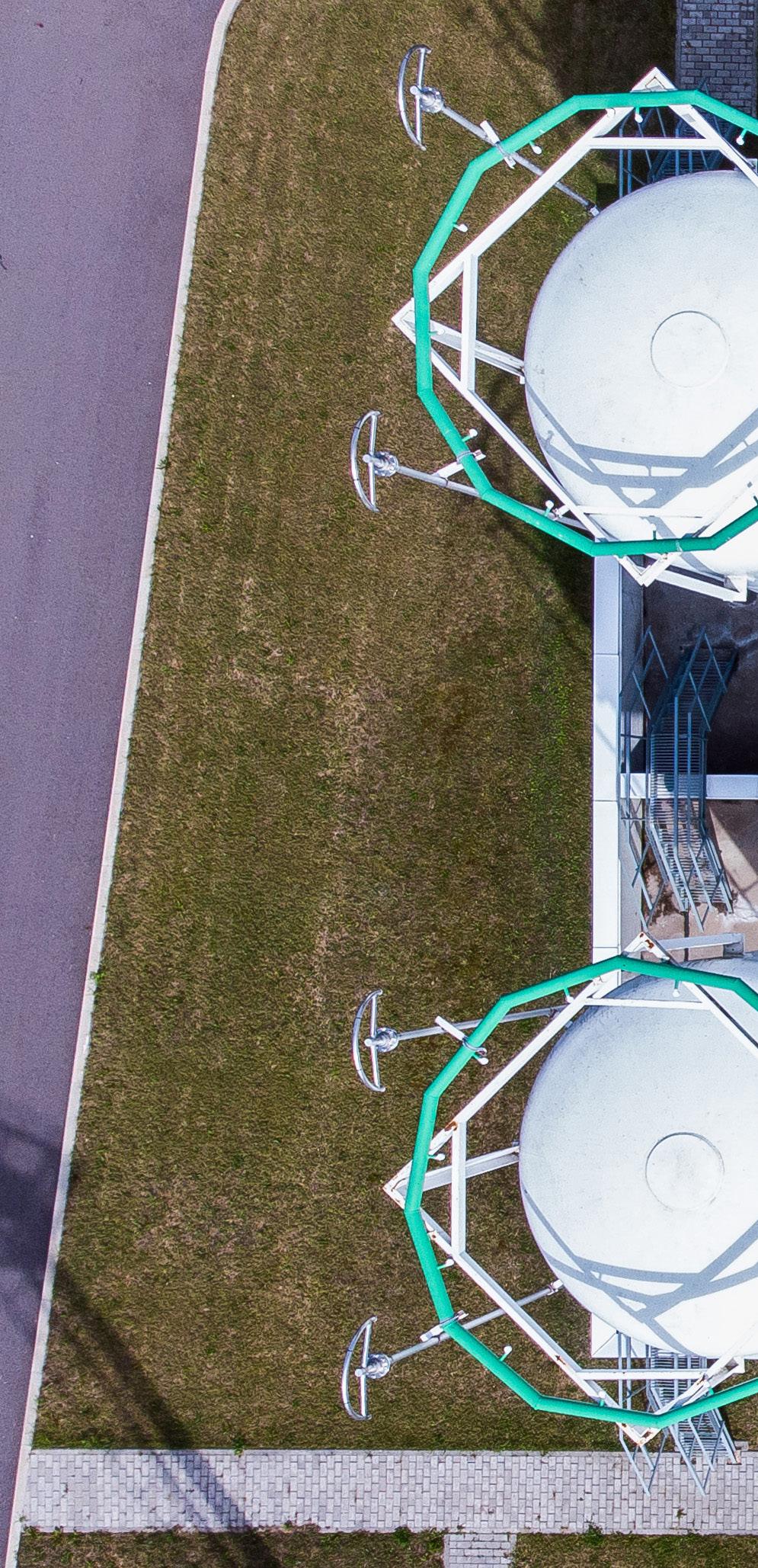
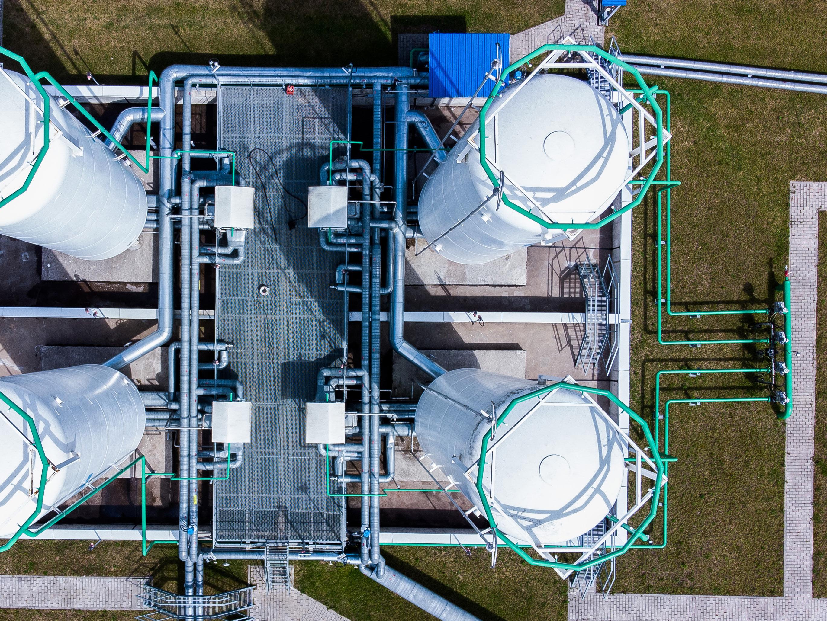
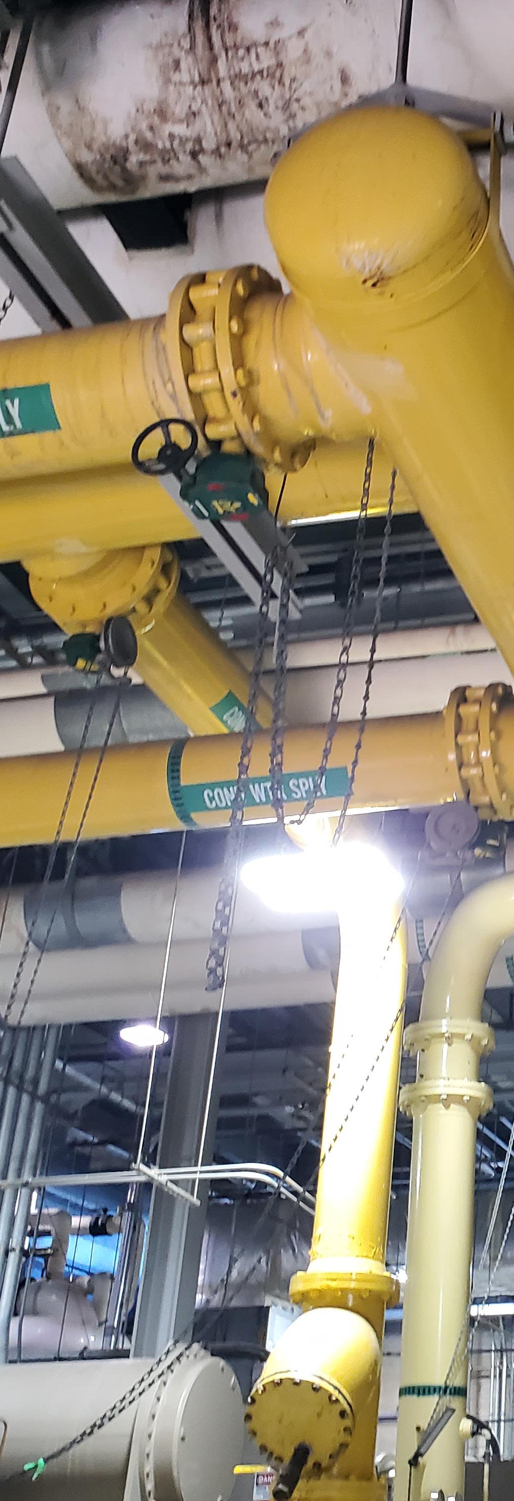
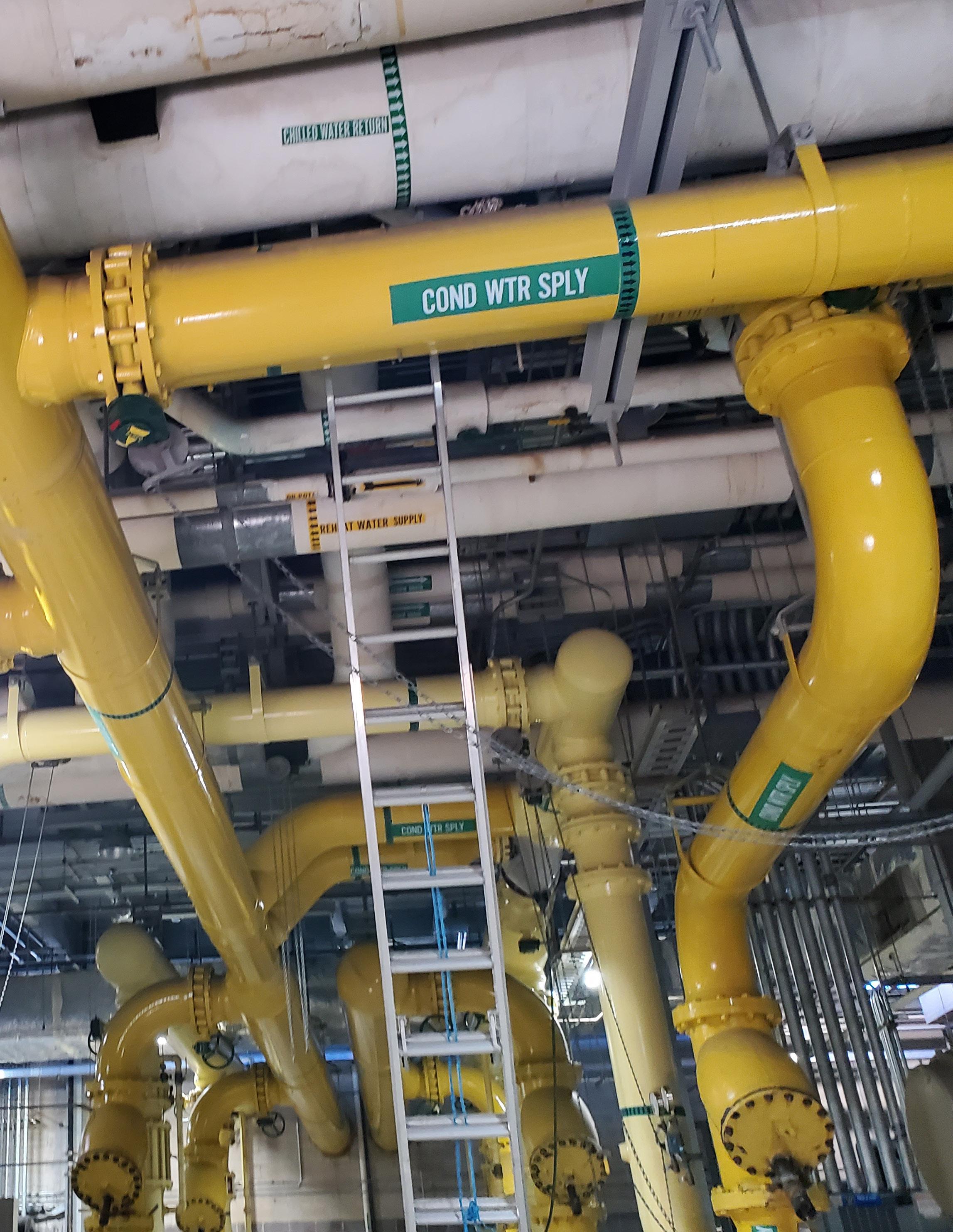
Process Utilities
Semiconductor
Solar
Tool Hookup
Water / Wastewater

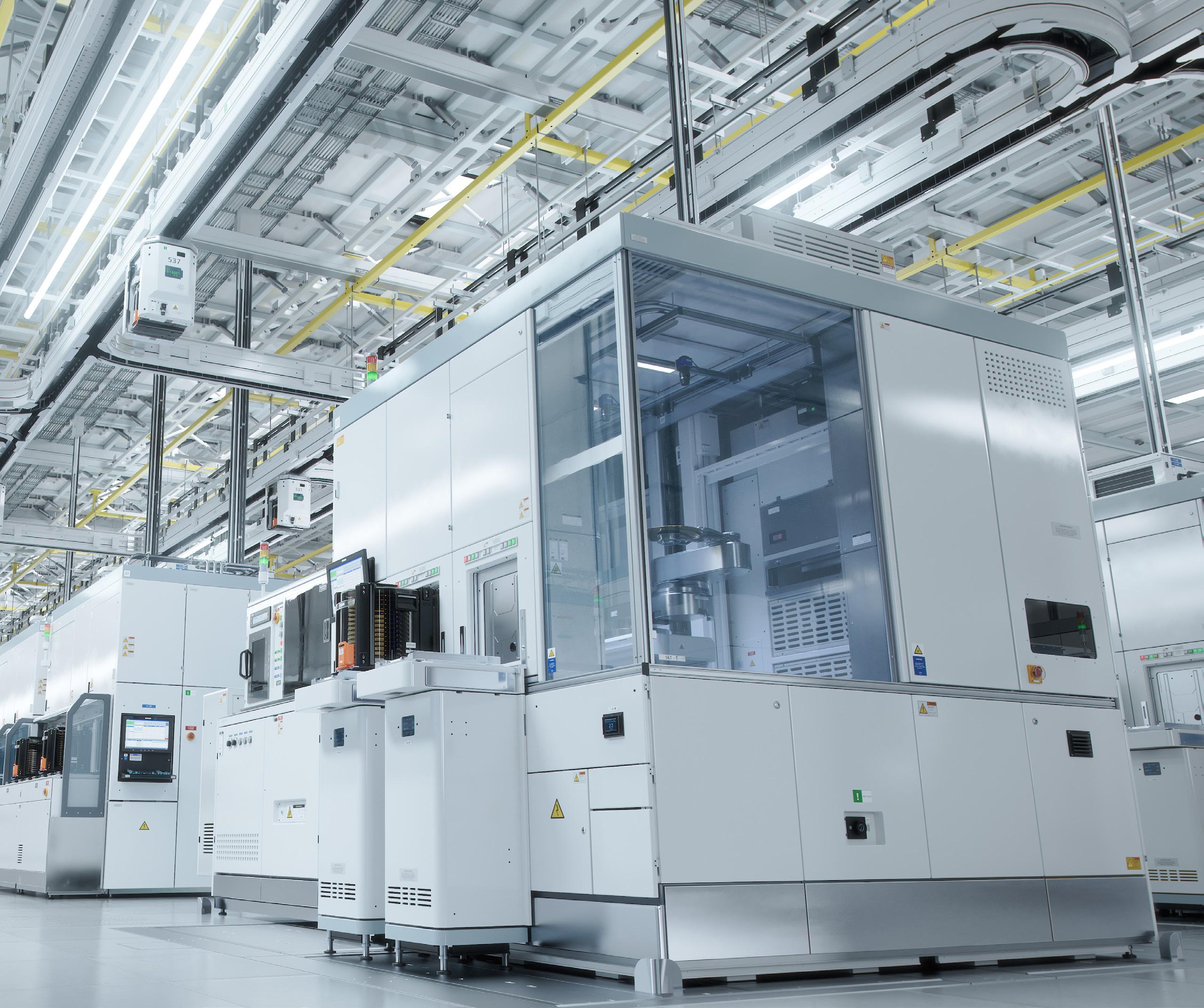
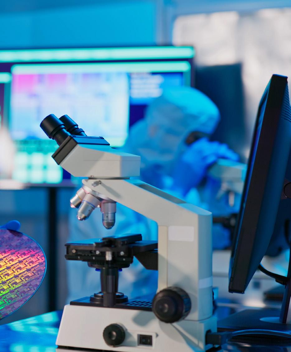
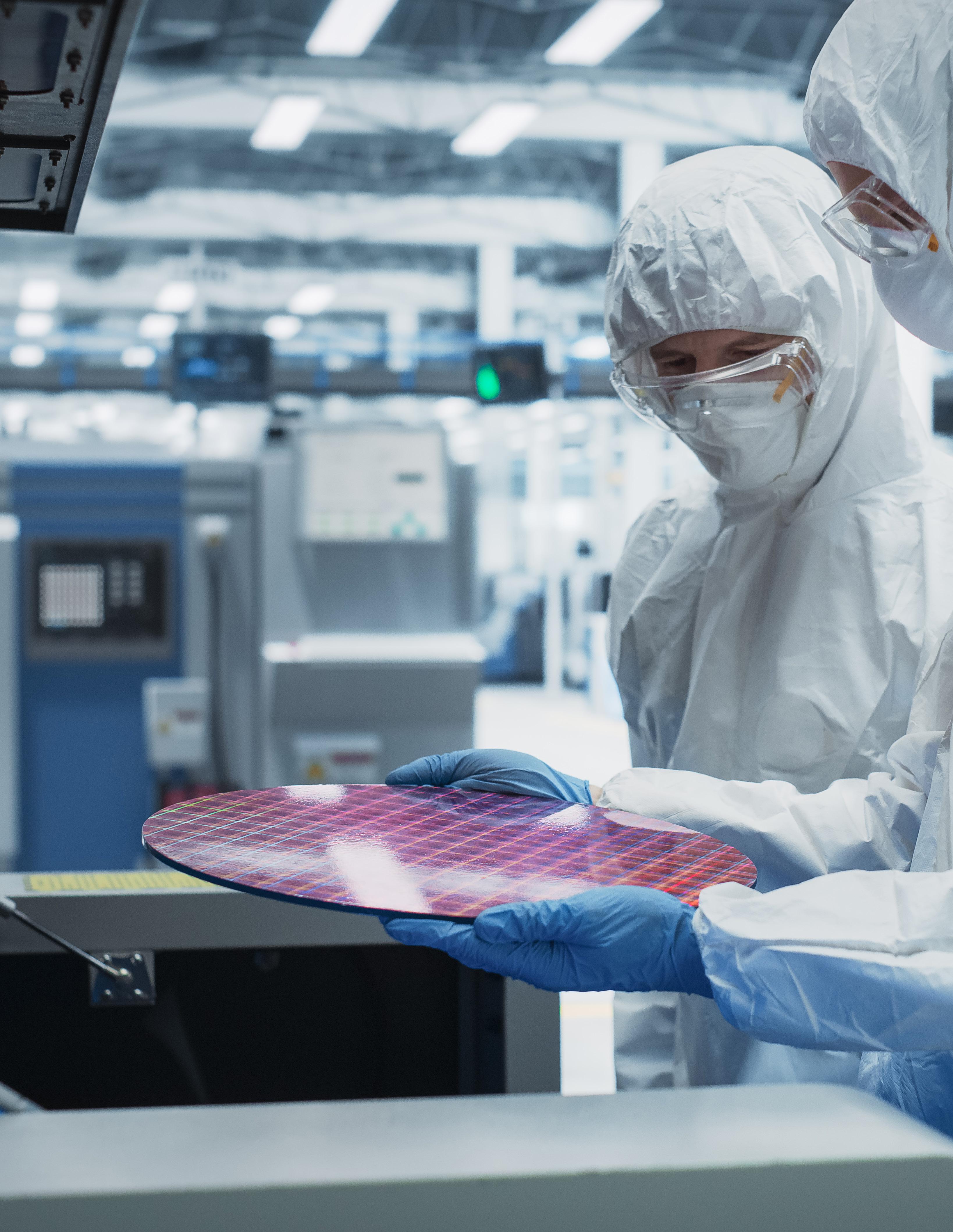
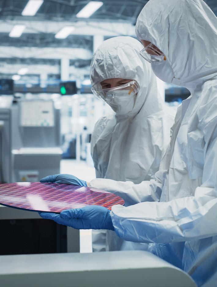
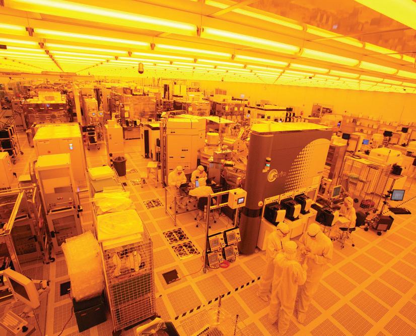
Semiconductors

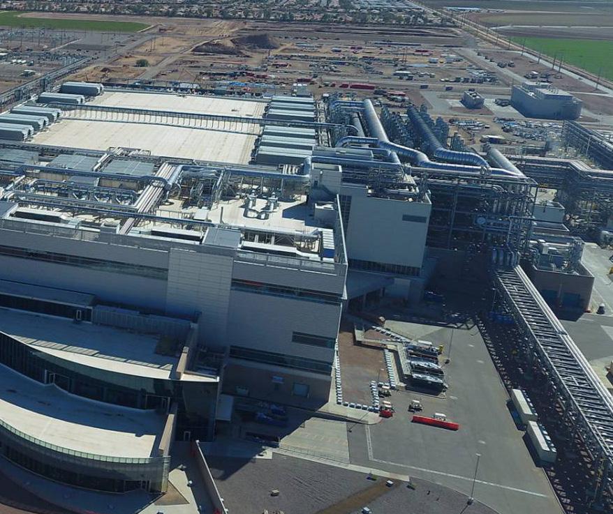
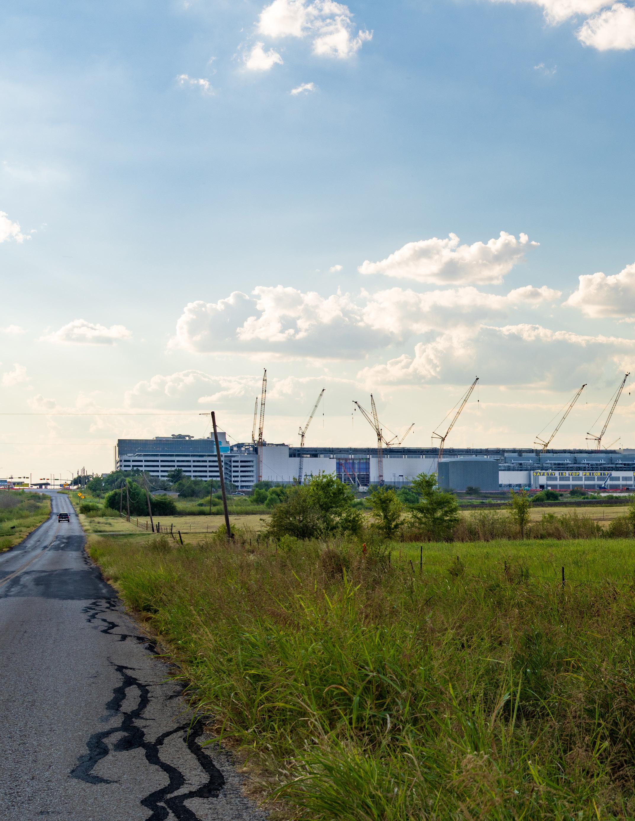
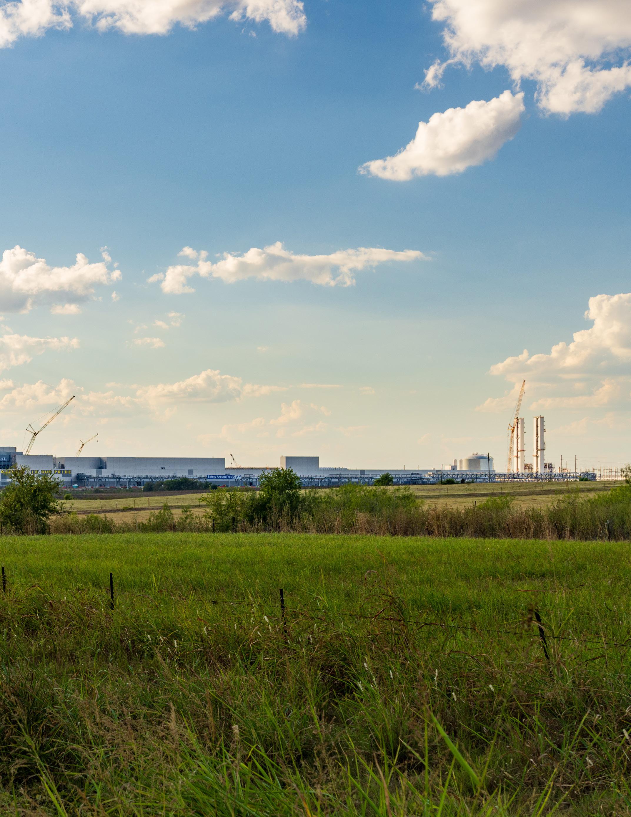
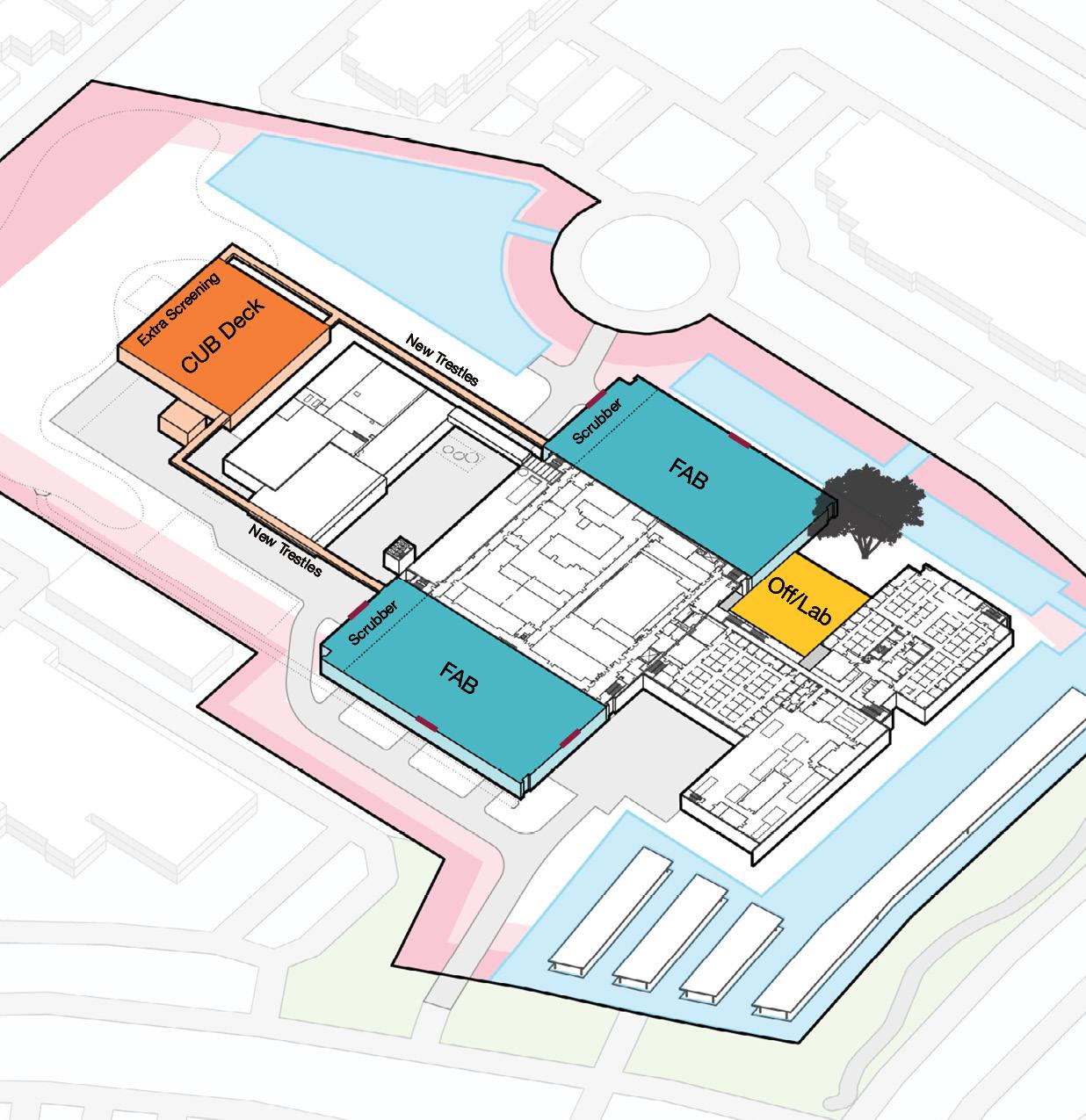
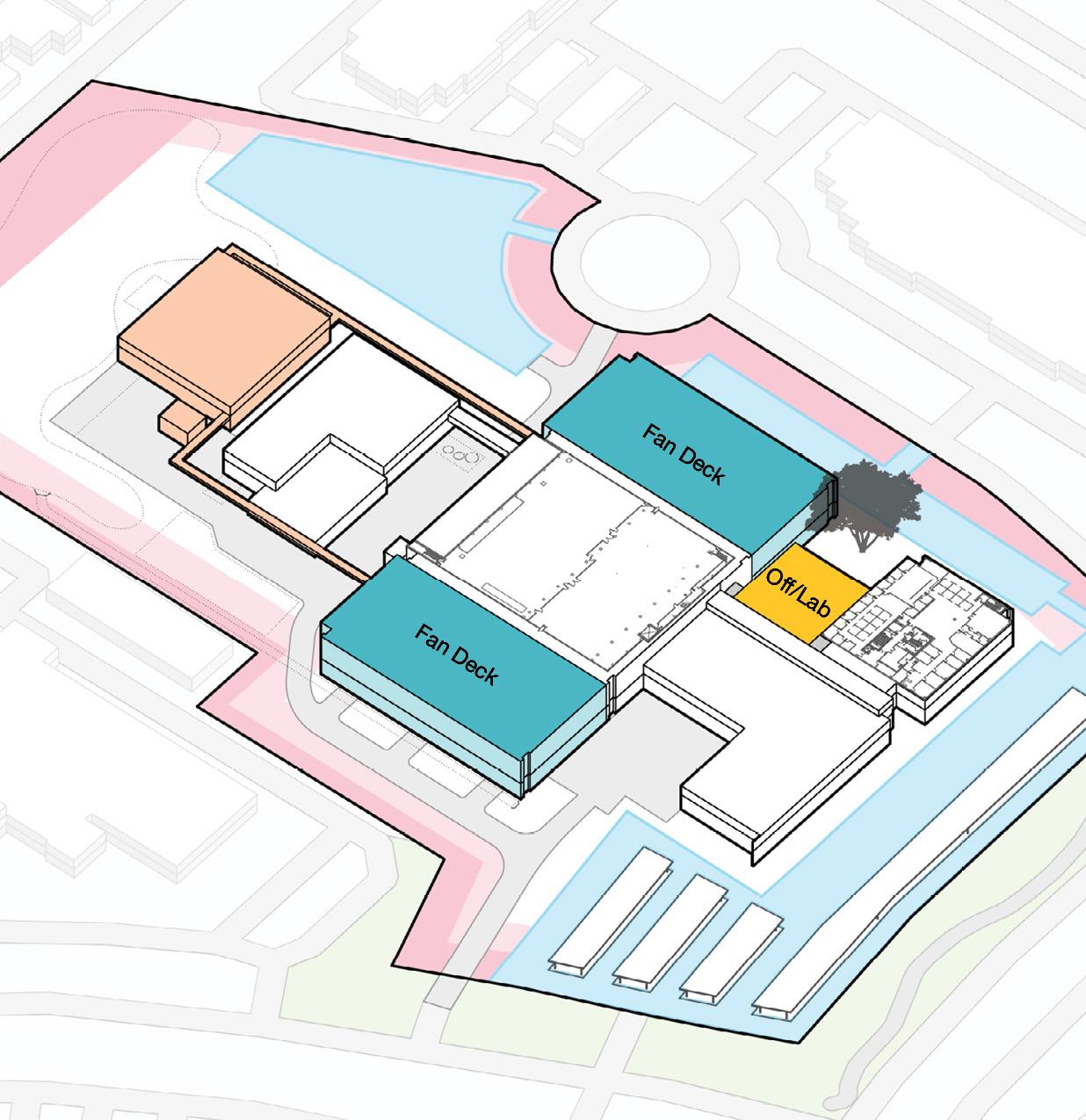
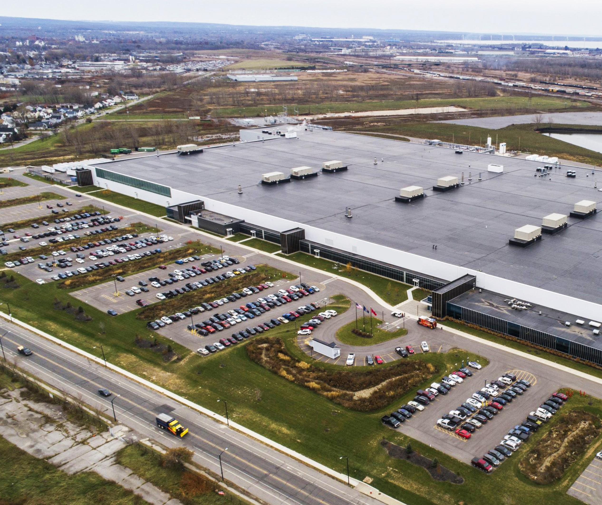
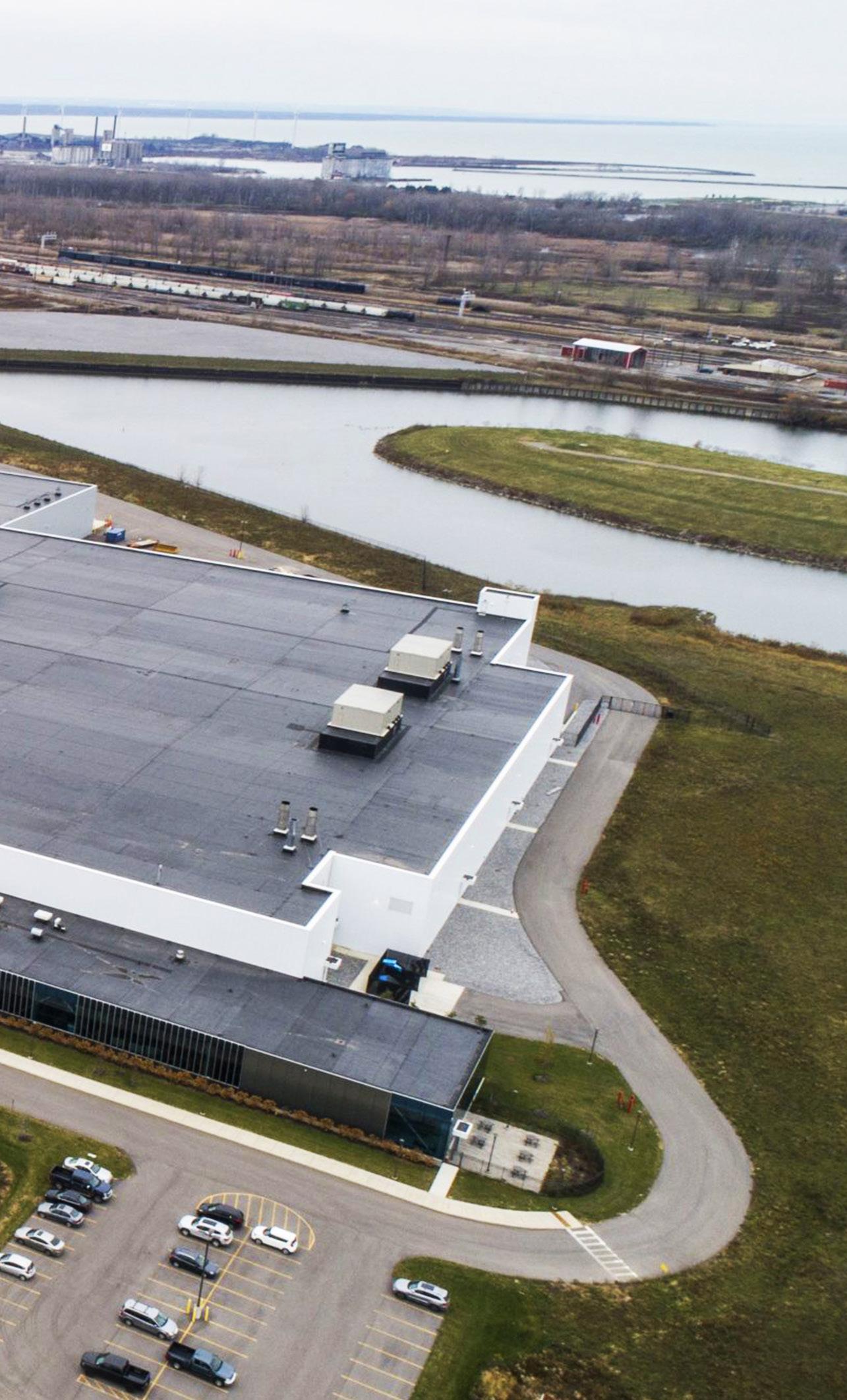
Confidential Wafer Manufacturer Building A
Phase 1
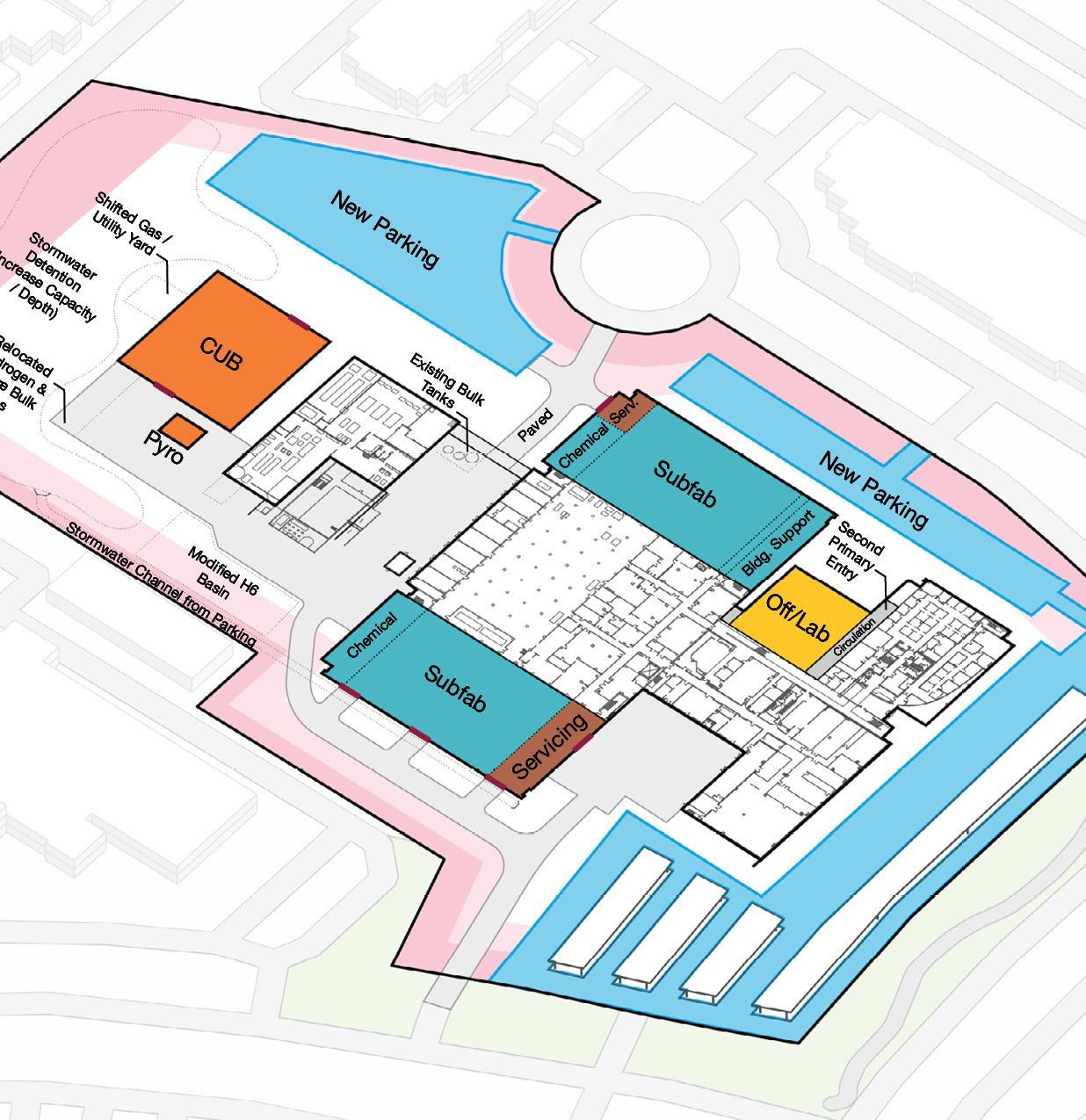
A new 300-millimeter silicon wafer manufacturing facility in North Texas represents a major advancement for the semiconductor industry and the regional economy. As the foundation of modern electronics, silicon wafers are essential to semiconductor fabrication. However, with the majority of wafer production occurring overseas, the U.S. has faced longstanding supply chain vulnerabilities.
This facility is the first of its kind in over 20 years, closing a critical gap in domestic manufacturing. By bringing wafer production back to the U.S., it strengthens supply chain resilience, reduces reliance on imports, and fuels innovation. This factory is a strategic investment in America’s technological leadership, ensuring the nation remains at the forefront of semiconductor advancements.
Services Provided
Architecture / Interior Design / MEP Engineering / Structural Engineering (Admin Bldg. & Central Utilities Building) / Commissioning
Relevancies
Fab / Central Utility Plant (CUP) / Admin Building / Water-Wastewater Treatment / Warehouse / Cleanroom
Services Provided
Architecture / Mechanical Engineering /
Electrical Engineering / Plumbing
Engineering / Process Engineering
Relevancies
Fab / Process Utility Building (PUB) / Process Systems Upgrades / Data Center
Size 121,093 SF
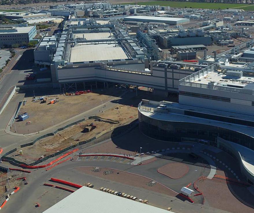
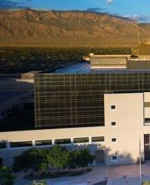
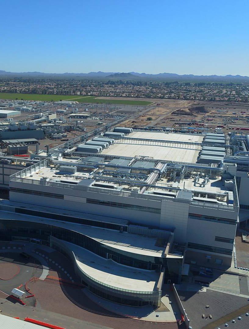
Ocotillo, Arizona
At the Ocotillo campus, our team has been a key partner in delivering architectural and engineering solutions through a design-build contract. Our work spans multiple upgrades, repairs, and alterations across the site, ensuring that existing facilities evolve to meet the demands of leading-edge semiconductor manufacturing. Executed in phases, these renovations integrate architectural, structural, and engineering disciplines to enhance operational efficiency. Notable projects at the campus include the MIT Data Center and PUB Expansion.
Gas/Chemical Layout and Facilitation – Managed project design and engineering for an $8M gas and chemical utility layout, optimizing equipment placement to align with process needs.
Facility Upgrade Services – Upgraded nitrogen, oxygen, and helium systems, along with ultrapure and cooling water infrastructure, to support advanced manufacturing. Expanded process recovery systems to increase capacity.
UPS Power Upgrade – Enhanced power reliability at two primary factories by installing additional UPS systems, achieving 100% redundancy.
Business Continuity Upgrades – Enhanced facility data reliability through design of a new backup data center.
Comprehensive Facility Upgrades – Delivered $24M in site-wide improvements, including process vacuum system validation, ultra-pure water capacity expansion, and highpurity gas distribution enhancements.
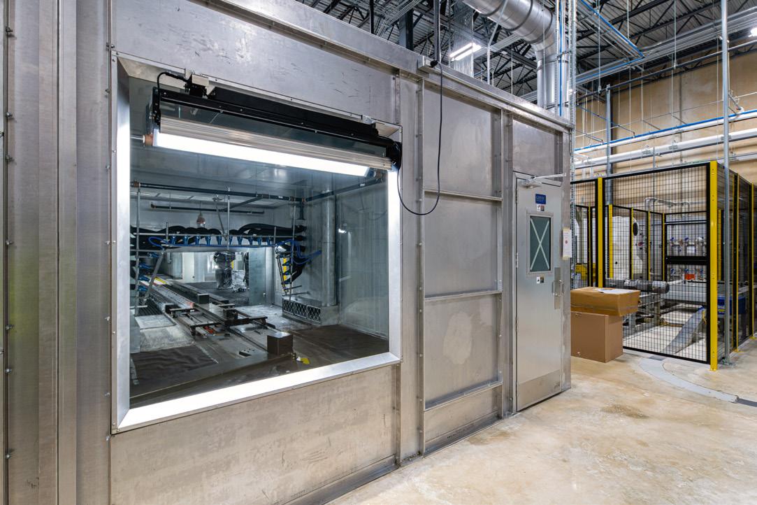
Confidential Advanced Packaging Facility
We provide comprehensive start-to-finish design services that include Gap Analysis, Positioning, Programming, Schematic Design, Detailed Design, Construction Documents, and Construction Administration for the retrofit, renovation, and conversion of three existing factories on this site. This scope of work encompassed a total of eight buildings, seven of which contained cleanrooms.
One of the factories underwent a complete retrofit, renovation, conversion, and expansion of a previously mothballed facility. This included an attached support building, an office building, and an expansion to accommodate the clean vestibule, airlock, and loading dock for the Die Sort cleanroom.
The state-of-the-art upgrades to the factories were aimed at enhancing operations for the manufacturing of advanced semiconductor packaging technologies, including the revolutionary 3D packaging technology known as “Foveros.” These upgrades supported new process tools with 14nm (1227) Passive Interposer, TSV Reveal, and C4 technologies, as well as Advanced Wafer Prep, Wafer Level Assembly, HOP Sort, Wafer Sort, Die Sort, Die Prep, Die Storage, and WLA Labs. Additionally, they ensured the ongoing operation of 32nm (1268) generation tools and Optane technology across four buildings of the two existing factories.
Services Provided Architecture of Record / Partial Process Engineering / Construction Administration / Construction Documents / Programming - Positioning - Gap Analysis
Relevancies
Fab / Cleanroom / Central Utility Building (CUB)
Sherman, Texas
Confidential Semiconductor Manufacturer SM1
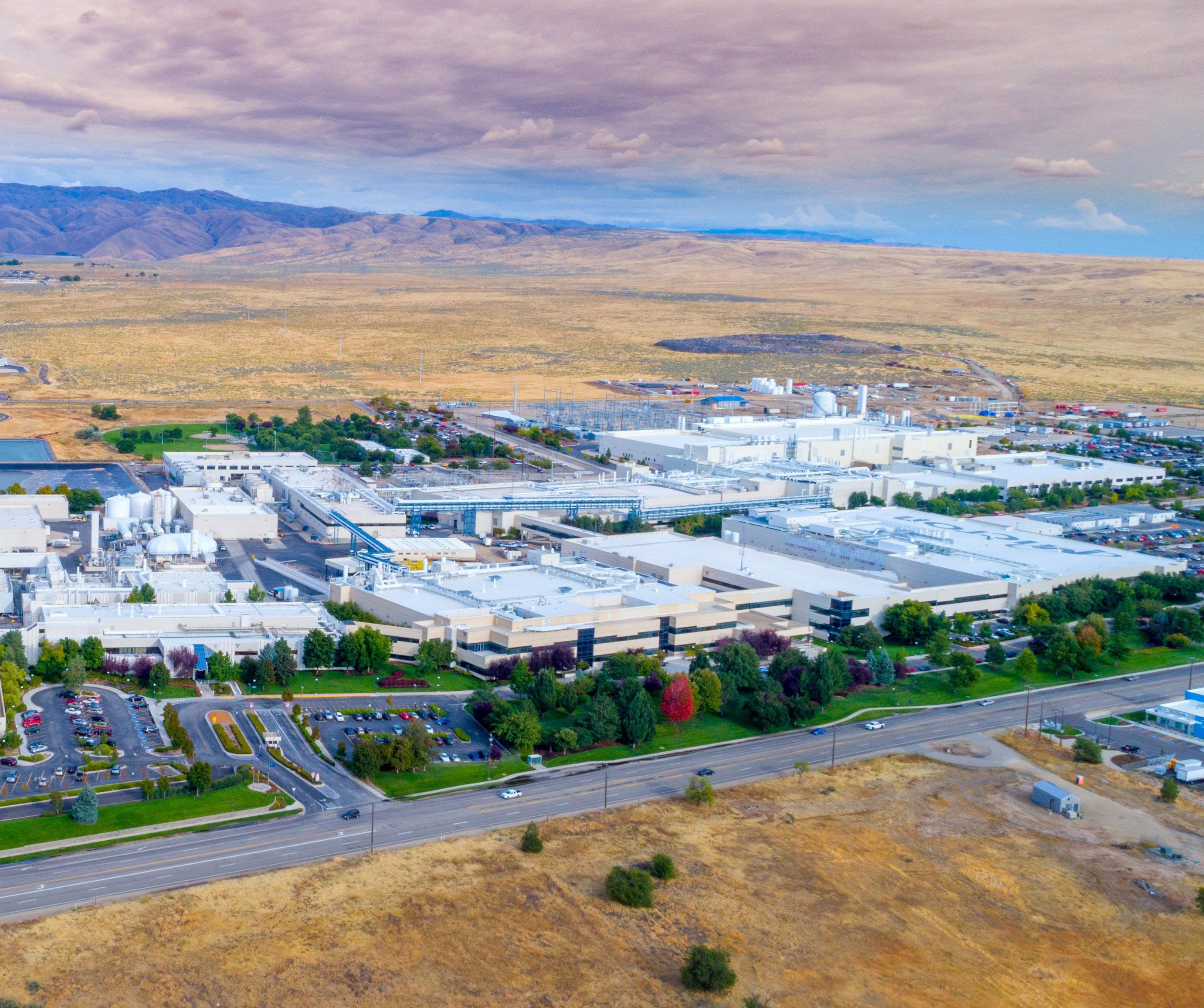
Page, now Stantec is providing architectural and engineering design for a next-generation semiconductor manufacturing complex on a 450-acre greenfield site in Sherman, Texas. The development includes four 300mm fabrication buildings, each 1.1 million square feet, featuring 400,000-square-foot cleanrooms, dedicated utility plants, and wastewater treatment systems. A central support building connects the FABs , optimizing workflow, while a separate office building provides space for 1,500 technicians, operators, and engineers, complete with dining, fitness, and recreation areas.
Designed for resilience, all buildings incorporate F3 tornadoresistant elements, on-site water storage, emergency power, fuel reserves, and shelter-in-place zones. The site includes a 1,500-space parking garage, a specialty gas facility, and dual power feeders from Oncor’s high-voltage grid.
Our full engineering and design services support a 10-year master plan, ensuring seamlessly phased implementation of all four FABs to drive long-term semiconductor manufacturing growth.
Services Provided
Master Planning / Architecture / MEP Engineering / Process Engineering / Structural Engineering / Interiors / Sustainability / Branding / Urban Design
Relevancies
Fab / CUP / Admin Building / Parking Garage / Cleanroom / VOC / Metrology Lab / Specialty Chemicals / Bulk Gas
Size
1,100,000 SF
Page, now Stantec
Boise, Idaho
Confidential Semiconductor Manufacturer Building
39 Central Utility Plant (CUP)
& Building 51X
At this Boise site, leading-edge infrastructure is the foundation for operational excellence and the expansion of highperformance semiconductor facilities. The Building 39 Central Utility Plant (CUP) & Building 51X projects exemplify strategic advancements that enhance efficiency, sustainability, and scalability—optimizing today’s operations while future-proofing for tomorrow’s breakthroughs.
Since the early 2000s, our longstanding partnership with this Confidential Semiconductor Manufacturer has been instrumental in driving continuous innovation and maintaining industry leadership. Through forward-thinking infrastructure solutions, we have built a resilient, adaptable utility framework that supports sustained growth and meets the evolving demands of semiconductor manufacturing. These investments reinforce a commitment to scalability, reliability, and the next generation of semiconductor excellence.
Services Provided Architecture / Mechanical Engineering / Electrical Engineering / Process Engineering / Fire Protection
Relevancies
Cleanroom / VOC / Space Management / Central Utility Plant (CUP) / Trestle / Water-Wastewater Treatment
Size
4,811,500 SF New Construction, Multi-Phased
Services Provided
Project Management / Architecture / Process Engineering / Mechanical Engineering / Electrical Engineering / Code Analysis / Structural Engineering / Civil Engineering / Landscape / Telecommunications / Fire Protection / Plumbing Engineering / Branding & Graphics / Building Performance Analysis / Commissioning / Interior Design / Lab Planning / Planning / Urban Design / Strategies & Analytics
Relevancies
Fab / GCS / Cleanroom / Metrology Lab / Wastewater Treatment / Warehouse / Chemical Storage / Emergency Response / Hazardous Waste / Specialty Chemical / Bulk Gas / Gas Yard / Hydrogen Chloride (HCl) / Silane (SiH4) / Utility Bridge / Control Building
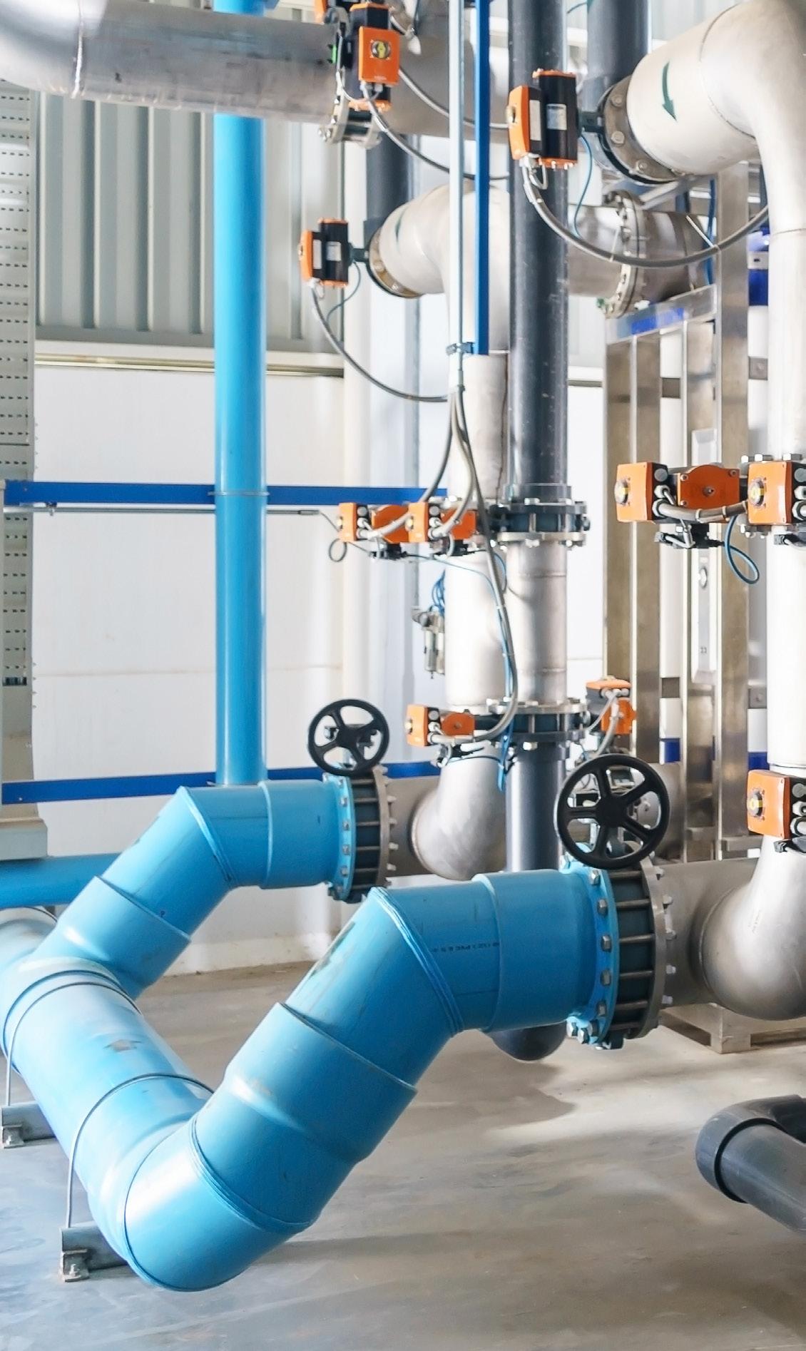
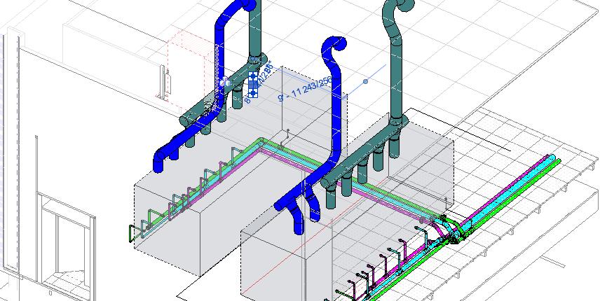
Gas, Chemical & Slurry (GCS) Systems
As part of the Gas, Chemical & Slurry (GCS) Systems scope, we developed storage and distribution systems for a new greenfield fabrication facility. This involved the precise design of specialty gas and process chemical handling, including waste chemical management. We provided extensive technical services such as chemical classification, equipment layout, utility hookup design, system sizing calculations, and advanced modeling for piping flow and stress analysis. These elements were critical in securing necessary permits and ensuring smooth construction execution.
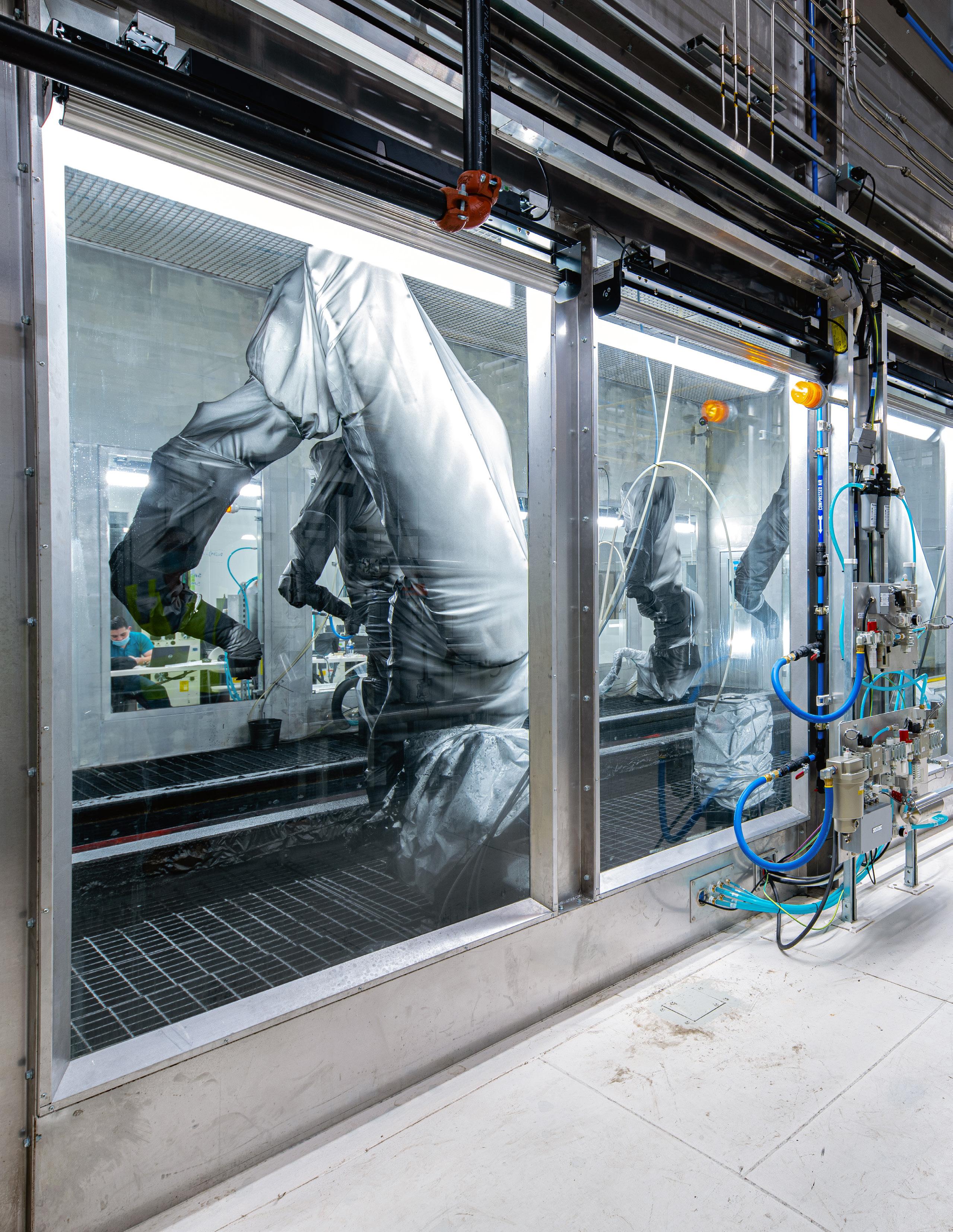
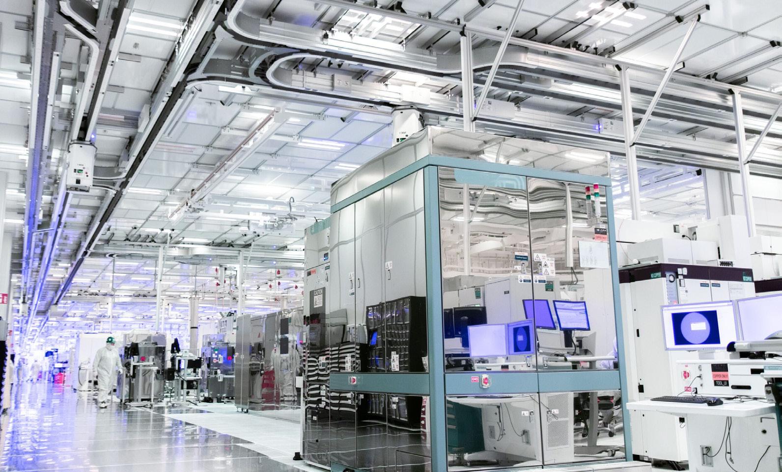
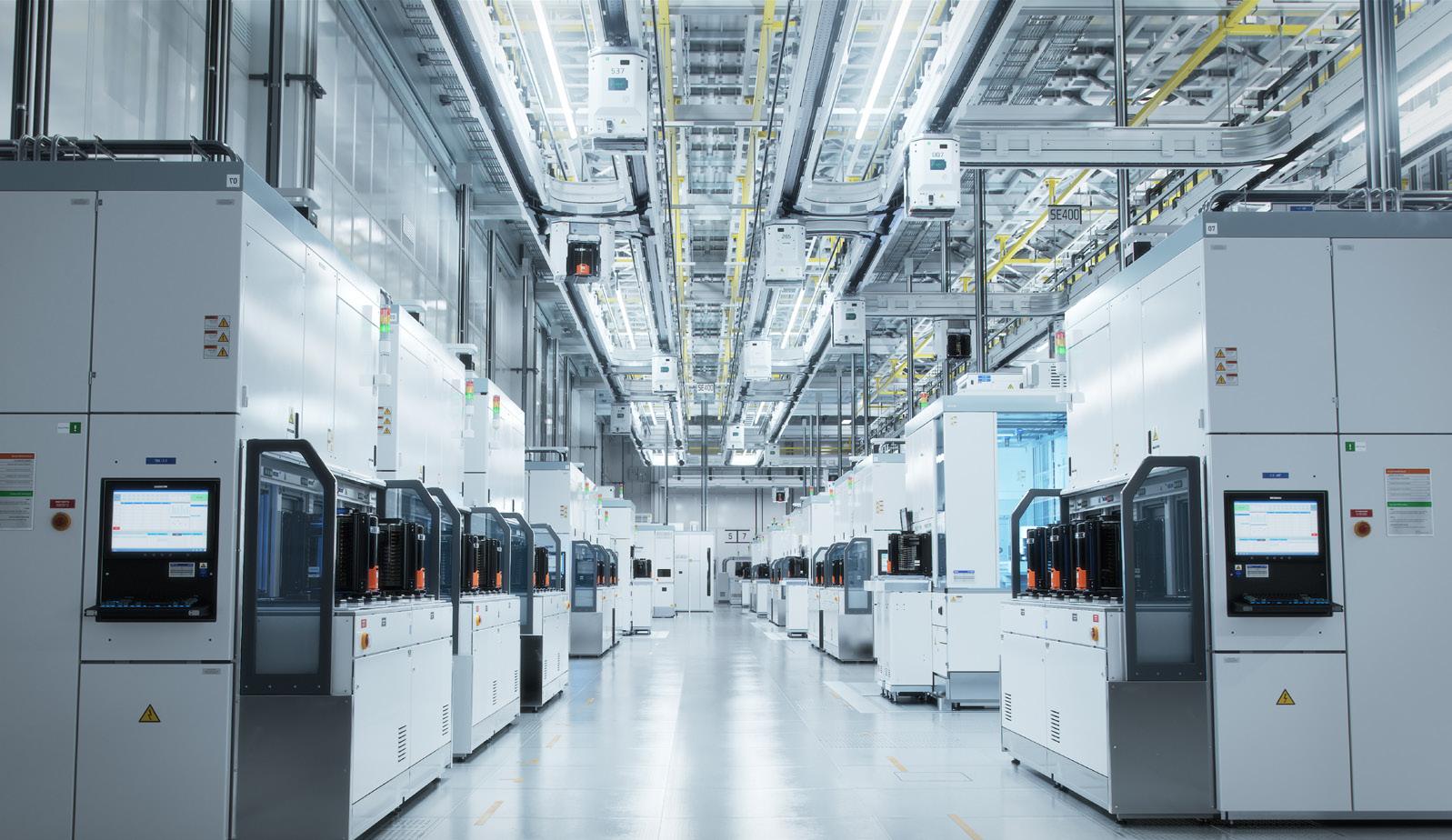
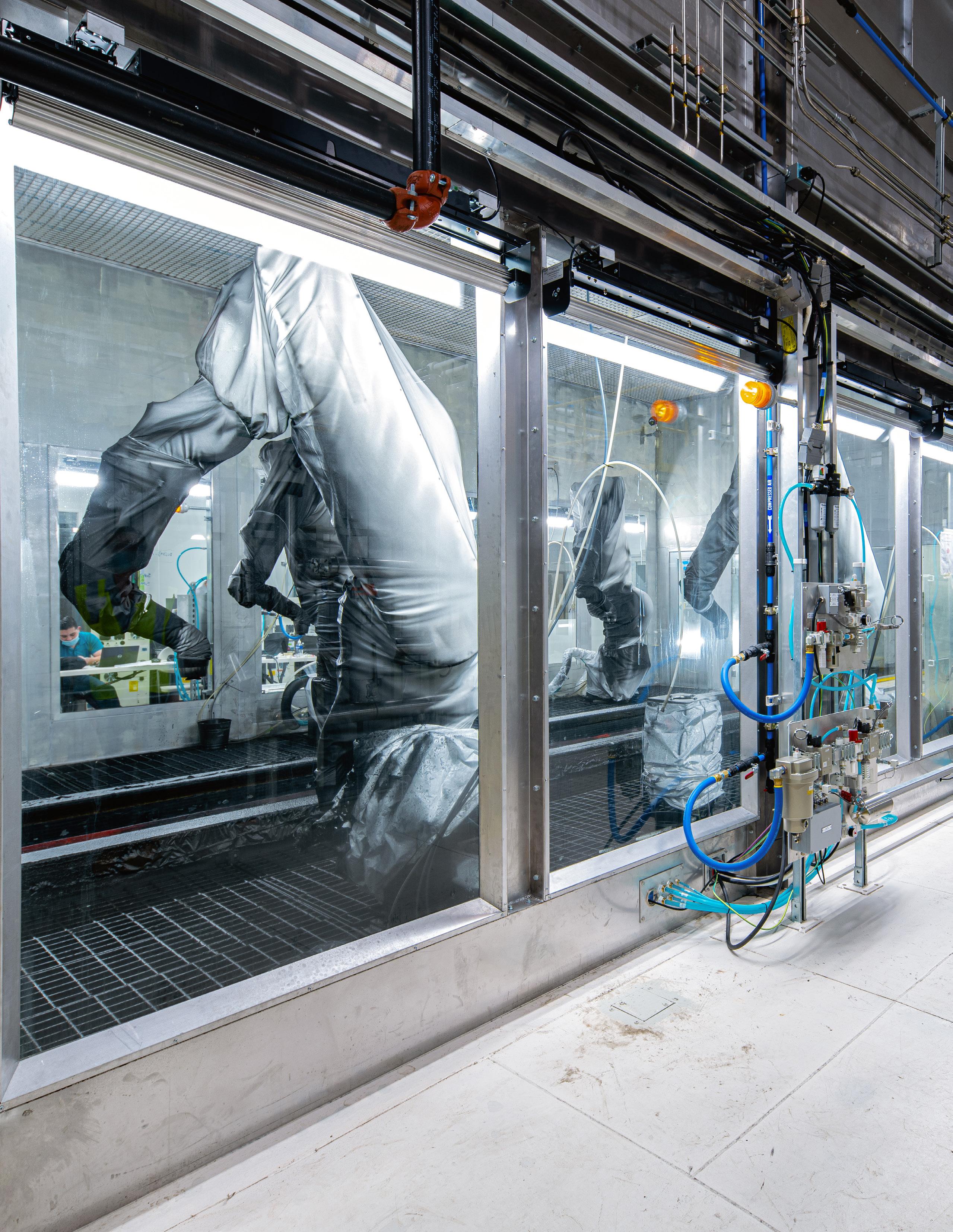
Cleanroom
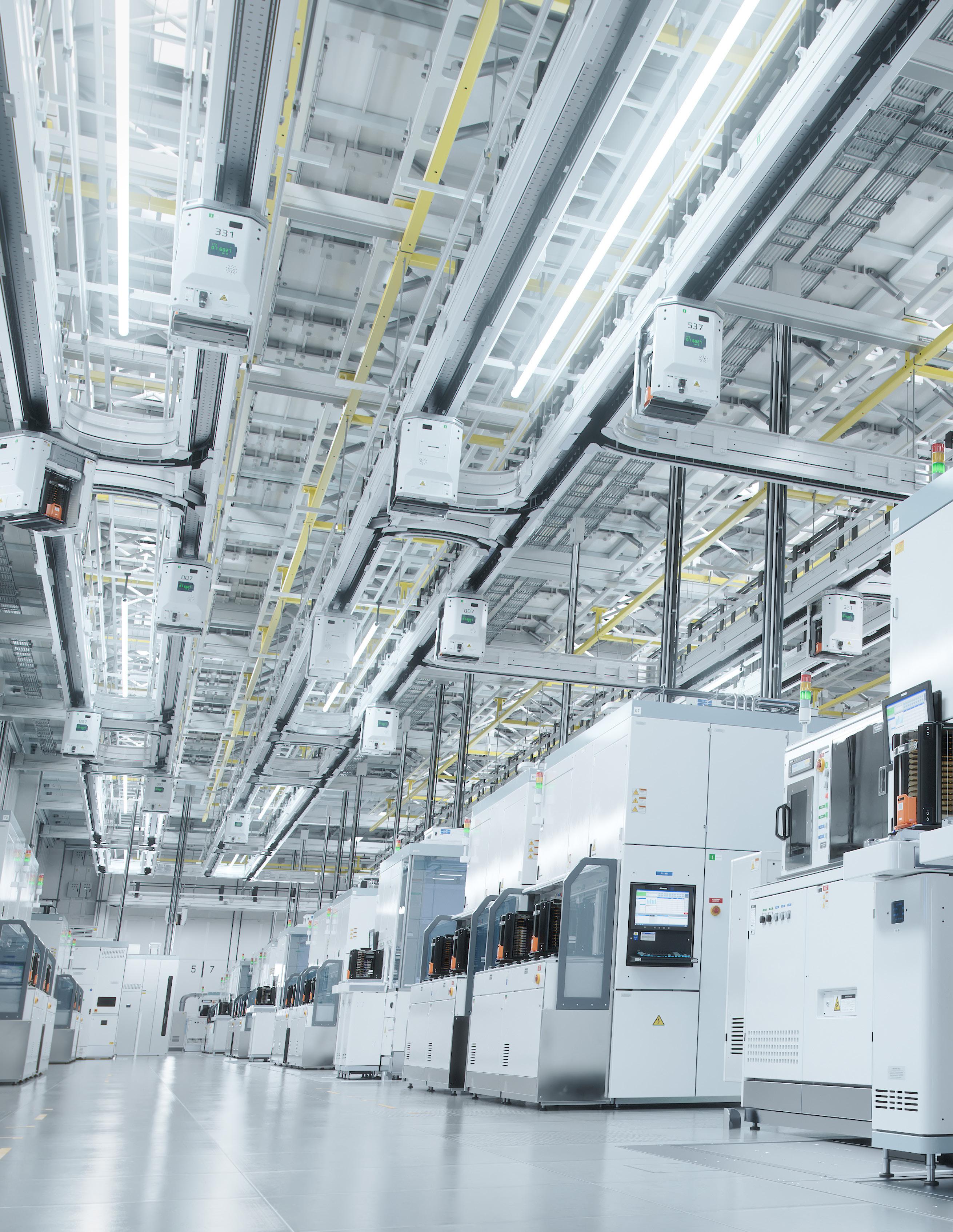
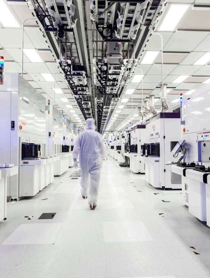
FAB1 boasts 1.2 million square feet of class-1 cleanrooms, including Fabrication and Sub FAB areas. As engineer of record, our team led architecture, structure, mechanical, process, electrical, and I&C work. We provided engineering analysis, managed permitting, attended client meetings, and oversaw construction. The cleanroom package included 3,000+ construction drawings.
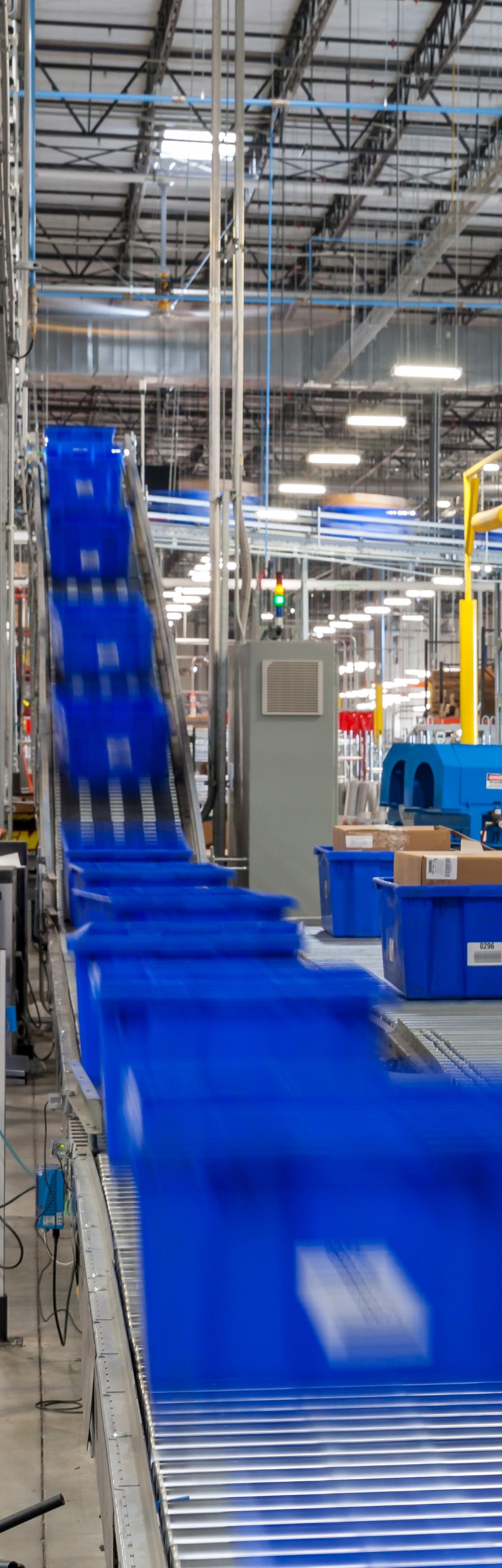
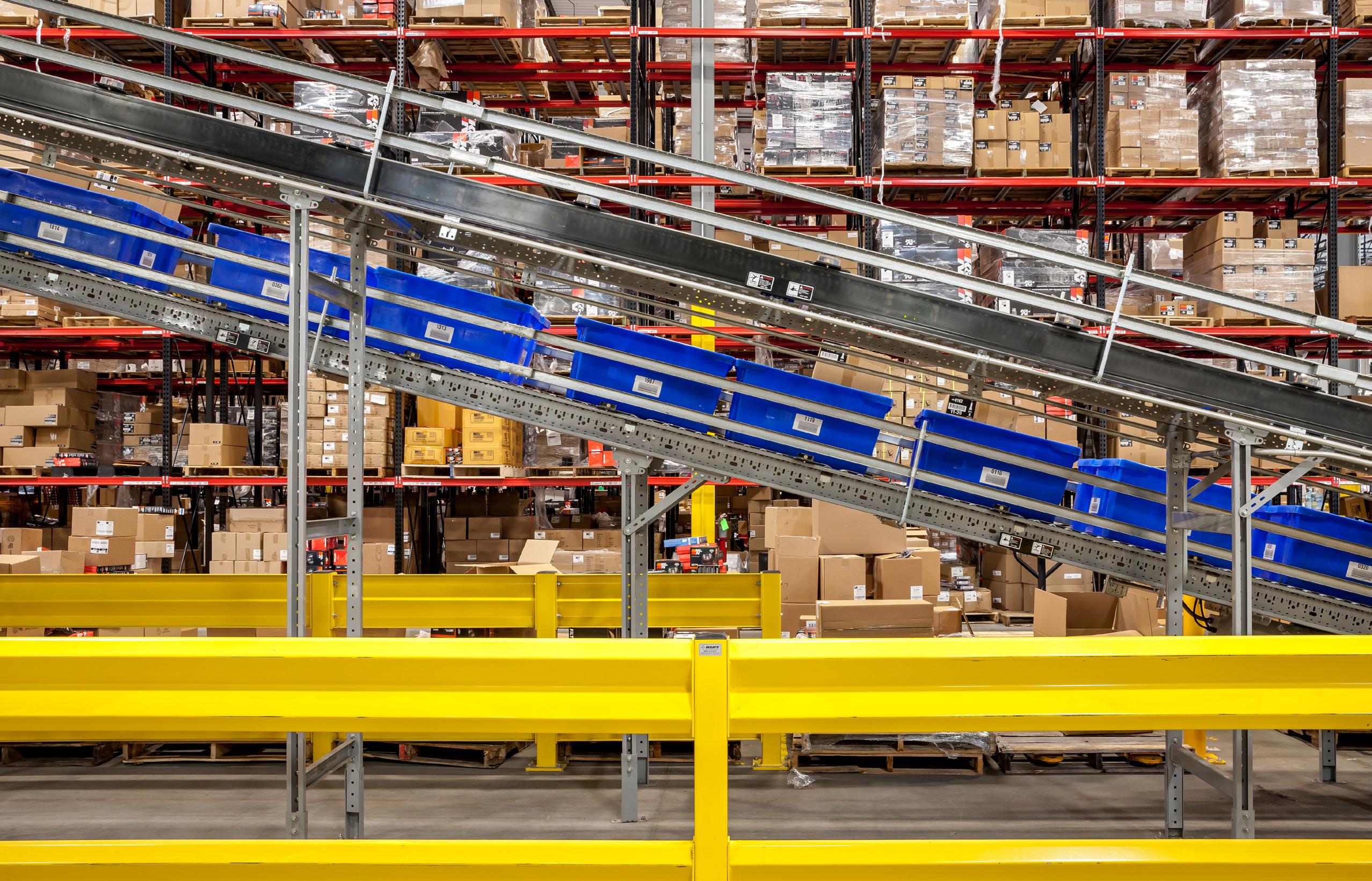
Warehouses
Beyond the fabrication infrastructure, we led the development of warehouse facilities, comprising eight buildings with a total footprint of 280,000 square feet. These warehouses serve vital functions, including secure chemical storage, emergency response, hardware innovation, waste segregation, and hazardous waste management. The Hardware Innovation Center provides space for research and prototyping, while the Wafer Granulator supports production efficiency. To enhance overall site functionality, We provided civil and landscape design, electrical and mechanical engineering, fire protection planning, and permitting services.
Designed for efficiency and safety, the facility integrates a Chemical Warehouse for secure storage, an Emergency Response Center for rapid incident management, and a Hardware Innovation Center for R&D and prototyping. Waste Segregation and Hazardous Waste facilities ensure responsible byproduct handling, while a Wafer Granulator, Gate House, and Guard Shack enhance security and operations.
Bulk specialty gas (BSGS) & ISO Yard
The Bulk Specialty Gas (BSGS) & ISO Yard was developed as a turn-key project within a broader campus initiative to support semiconductor production. This facility enables the manufacturing of advanced logic chips used in high-performance computing, 5G, and artificial intelligence applications.
Key features include:
Integrated Control Buildings: three dedicated buildings for real-time monitoring and management.
Specialized ISO Canopies: six canopies designed for safe handling of H2/N2, SiH4, NH3, He, N2O, and NF3 gases.
Dedicated HCl and CO2 Facilities: HCl ISO building and CO2 tank with supporting equipment pad.
Grade-Supported Equipment Pads: stable foundation ensuring safety and operational integrity.
Multi-Level Utility Bridge: Optimizing connectivity across facility infrastructure.
Layout Dependent Design Capabilities
Albuquerque, New Mexico
Sandia National Laboratories Tool Hookup
Our team provided process engineering design services and prepared comprehensive construction documents to support the Silicon Fab Life Extension Project at Sandia National Laboratories (SNL) Building 858N. The project scope focused on advancing semiconductor manufacturing capabilities by upgrading the facility from 6-inch to 8-inch wafer production.
Key Project Components:
Manufacturing Process Upgrades:
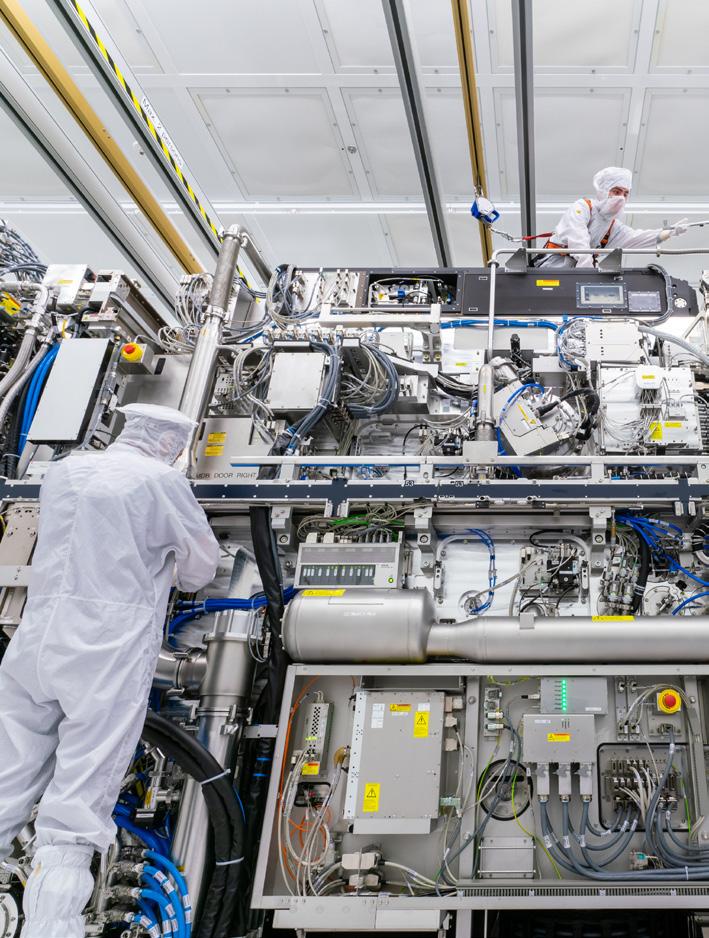
Designed and integrated approximately 45 new or upgraded tools, including CMP, Diffusion, Etch, Implant, Lithography, Wets, CVD, Microscopes, and Metrology systems.
Supported the relocation of 15 Metrology tools and coordinated the removal of 61 legacy tools, including Lithography, Metrology, Diffusion Furnaces, Wet Benches, and Scopes.
Facility Renewal and Upgrades:
Developed process design solutions for facility renewal, replacement, and infrastructure upgrades to accommodate the transition to 8-inch wafer manufacturing tools.
Addressed mechanical, electrical, and process utility requirements to ensure seamless integration of new and relocated equipment.
Innovative Design Approach:
Employed laser scanning technology to capture the interior and exterior of Building 858N.
Produced highly accurate as-built models of equipment, piping, and conduit to support precise design coordination and minimize construction conflicts. The design solutions delivered through this project enabled Sandia National Laboratories to modernize semiconductor manufacturing capabilities, extend the operational life of Building 858N, and provide a flexible infrastructure platform to support future technology advancements.
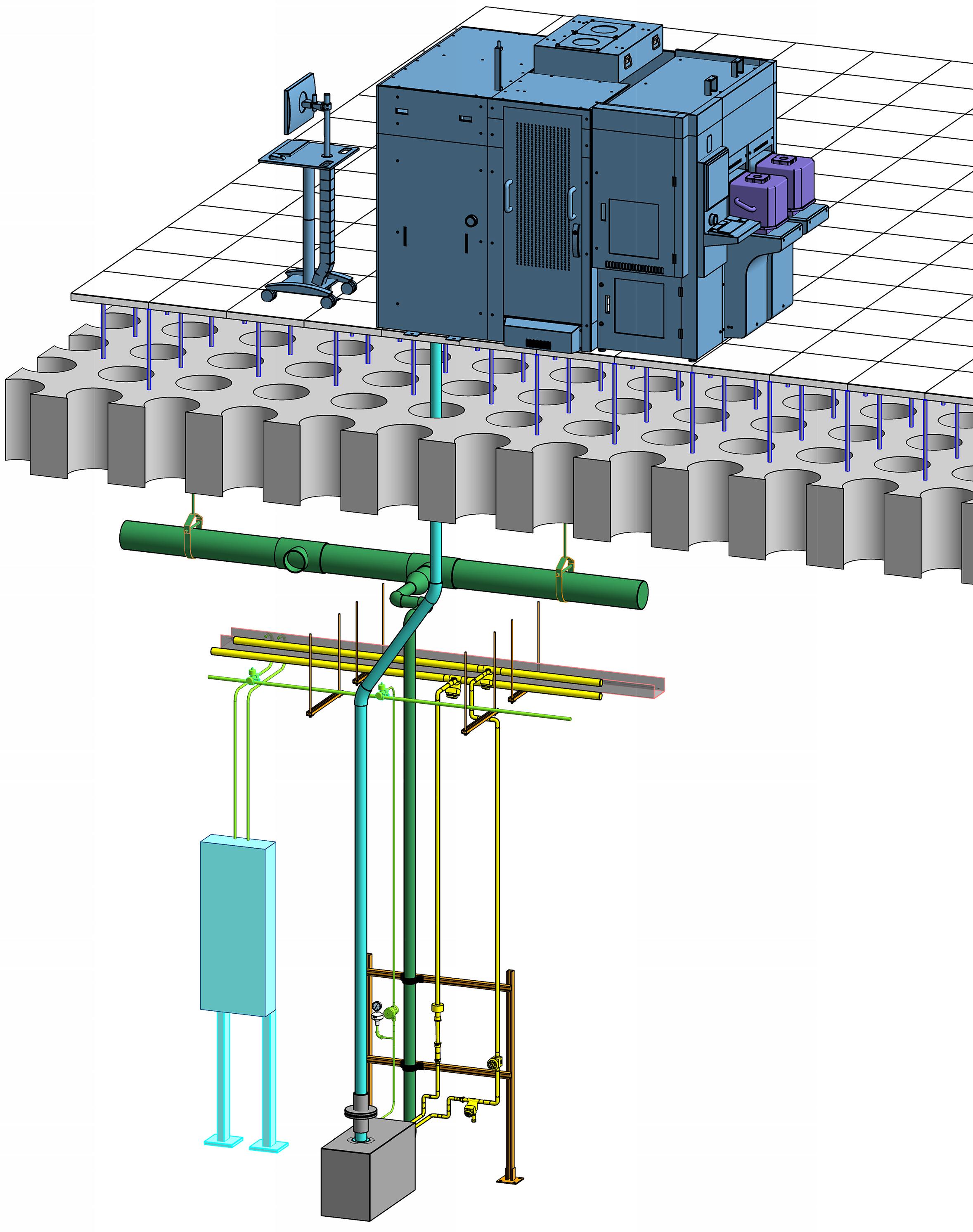
Confidential Semiconductor Manufacturer Layout Dependent (LOD) Design
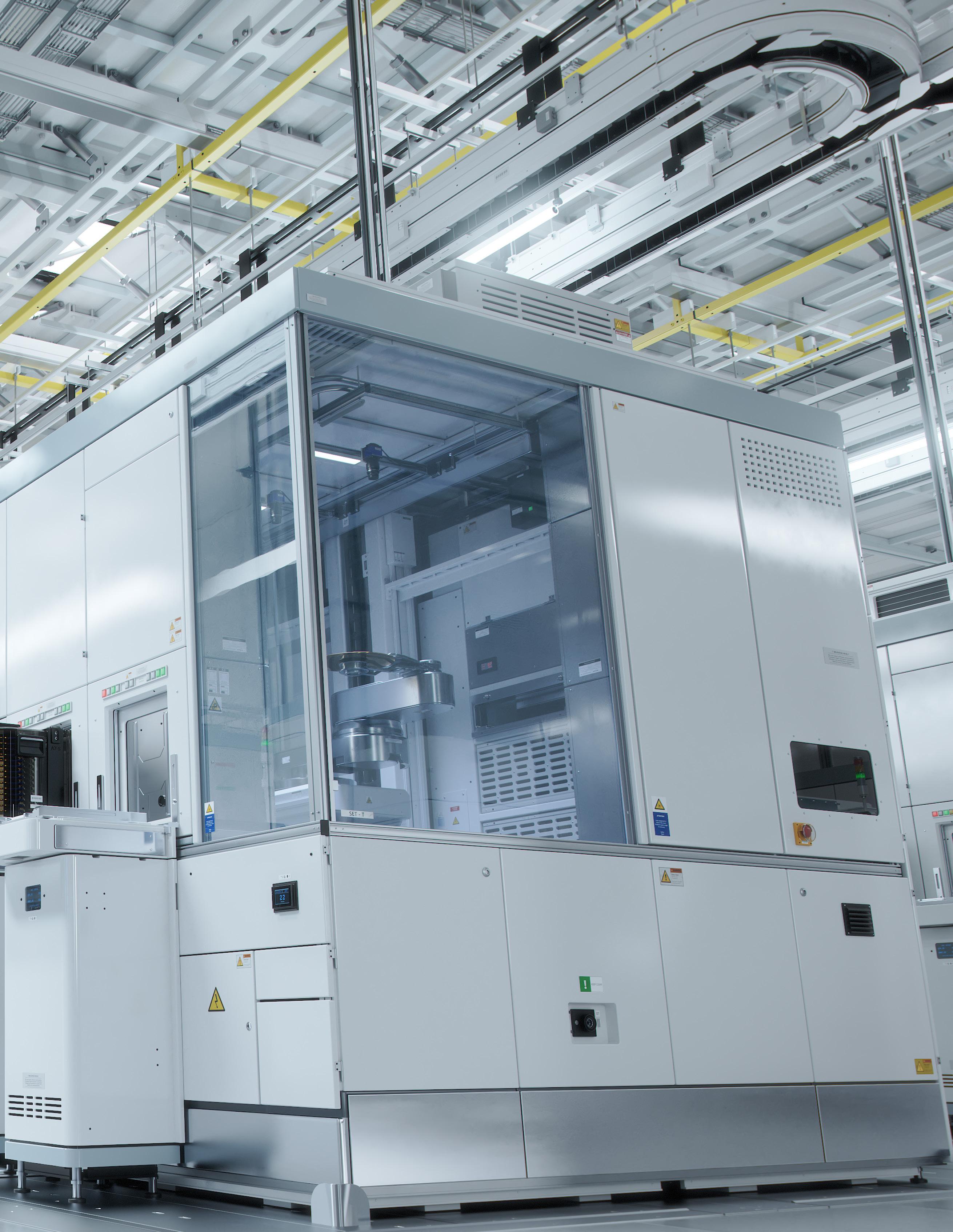
Our team provided layout-dependent (LOD) utility design services to support the installation of semiconductor production tools within the fab environment. The work included sizing, designing, and routing of piping and duct laterals, as well as points of connection (POCs) for mechanical and process systems, tailored to the specific layout and configuration of each tool bay. Systems addressed included process cooling water (PCW), ultrapure water (UPW), clean dry air (CDA), process gases, exhaust, vacuum, and chemical distribution. Designs were closely coordinated with tool utility models and facility constraints to ensure reliable integration and optimal tool performance.
Arizona
ASU MacroTechnology Works Equipment Install
The project encompassed the design and layout development for Rooms 2305 and 1512, including final tool layout plans, utility routing drawings with Facility Points of Connection, utility laterals, one-line electrical diagrams with load calculations, electrical panel schedules, and power plans, along with Unistrut rack and raised access flooring details. For Room 1512 specifically, the scope included installing a new cleanroom ceiling, updated flooring, repainting, oversized entry doors, and modifications to lighting, telecom, security, HVAC, and fire alarm systems, as well as utility connections for equipment installation. Additional work involved selective demolition of part of the existing hollow metal glazing system, removal of a wing wall, and relocation of the Janitor Closet and mop sink to an adjacent space near Room 1430—all aimed at enhancing functionality, efficiency, and aesthetics.
San Antonio, Texas
Confidential Semiconductor
Manufacturer Building 1
Bay 2H Tool Install
This project involved providing comprehensive design services for the installation of tools in Building 1, Bay 2H. This project consisted of multiple tool install packages for a cleanroom space that we also completed the design for. The scope included developing complete tool installation packages with multidisciplinary engineering support. The wchemical services, along with instrumentation and controls as required. The tool install packages included facility documentation (cover sheets, data sheets, fab tool layouts), general notes and assumptions for each discipline, specialized systems including a CO2 suppression system, as well as hook-up drawings and details for each system.
Tempe,
New Mexico
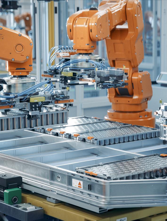
Confidential Battery
Manufacturer BMC1 CAM2
Tool Install
We delivered a fully integrated tool install design for the CAM2 facility, coordinating architecture, electrical, mechanical, plumbing, process, telecom, and security systems into a unified solution. The final package incorporated scope for detailing tool hook-ups, including all MEP points of connection for tooling equipment within the Cathode Active Material (CAM2) facility. Through close cross-discipline collaboration, the project achieved a safe, efficient, and scalable design that meets current operational needs while supporting long-term growth.
Confidential Semiconductor Manufacturer Layout Dependent (LOD) Design
Our team provided layout-dependent (LOD) utility design services to support the installation of semiconductor production tools within the fab environment. The work included sizing, designing, and routing of piping and duct laterals, as well as points of connection (POCs) for mechanical and process systems, tailored to the specific layout and configuration of each tool bay. Systems addressed included process cooling water (PCW), ultrapure water (UPW), clean dry air (CDA), process gases, exhaust, vacuum, and chemical distribution. Designs were closely coordinated with tool utility models and facility constraints to ensure reliable integration and optimal tool performance.
Sherman, Texas
Confidential Wafer
Manufacturer Tool Install
Page, now Stantec delivered comprehensive utility designs to support the manufacturing tools, ensuring seamless integration and reliability across critical facility systems. The scope of work encompassed power distribution, process chemicals and gases, process cooling water, clean dry air (CDA), process exhaust systems, and industrial wastewater management. Each utility was carefully engineered to meet the stringent requirements of advanced manufacturing operations, with a focus on efficiency, safety, and long-term sustainability.
Research & Development
Albany, New York
NY CREATES Albany NanoTech Complex
NY CREATES is the owner and operator of the Albany NanoTech Complex, the nation’s largest and most advanced non-profit semiconductor R&D facility. As a leading-edge hub for innovation, Albany NanoTech brings together industry leaders, academic institutions, and international partners to drive the development of next-generation chips and fabrication processes.
For more than two decades, this state-of-the-art complex has been at the forefront of groundbreaking advancements in semiconductor technology. Today, it continues to expand its global partnerships, attracting industry pioneers in the semiconductor market, energy efficiency and renewable energy technologies.
Our firm has played a pivotal role in shaping this visionary complex—contributing to the master plan and designing many of its advanced research facilities.
Services Provided
Programming / Master Planning / Architecture / Project Management / Engineering / Telecom / Security / Graphics / Sustainability
Relevancies
Research & Development (R&D) / Tools / Cleanroom / Specialty Chemical / Bulk Gas / Metrology Lab / Data Center
Pioneering the Future of Semiconductor Innovation
To support the Albany NanoTech Complex’s rapid growth, NY CREATES developed a Master Plan to guide its expansion. As the anchor of New York State’s Tech Valley, the Complex has become a global hub for semiconductor innovation, attracting 300+ industry and government partners with its world-class facilities and cutting-edge technology.
The master plan provided a strategic framework for three major phases of expansion, adding over 1 million square feet of state-of-the-art research and development space—more than doubling the size of the Complex.
Phase 1: NanoFab Xtension (NFX) – A significant expansion of cleanroom and R&D facilities.
Phase 2: Zero-Energy Mixed-Use Facility (ZEN) – A highperformance, energy-efficient research and collaboration space.
Phase 3: NanoFab Reflection – A current expansion aimed at enhancing advanced semiconductor research capabilities.
NanoFab Xtension (NFX): Advancing Semiconductor Innovation
The NanoFab Xtension (NFX) Building stands as a symbol of the power and promise of emerging technologies. As part of NY CREATES, a world leader in nanoscience R&D and education, NFX houses more than 120 wafer processing and inline metrology tools, supporting the development of next-generation semiconductor manufacturing.
Class 1,000 cleanrooms enable leading-edge research and production of the most advanced chip manufacturing tools. Specialized structural features support heavy manufacturing equipment and mitigate vibrations. The facility also hosts 300mm advanced lithography platforms, including 193nm immersion and EUV lithography, along with technologies for planarization, copper plating, etch development, ion implantation, thin film deposition, and wet cleaning.
NFX is a 500,000-square-foot facility, featuring 55,131 square feet of cleanrooms, solidifying its role as a cornerstone of semiconductor research and innovation.
Zero Energy Nanotechnology Building (ZEN)
The Zero Energy Nanotechnology (ZEN) Building is a groundbreaking 363,000-square-foot mixed-use facility— the largest zero-energy-capable building of its kind in the United States at construction completion. Located within a dynamic research environment that hosts 3,000 scientists, engineers, faculty, students, and staff, ZEN serves as a hub for innovation, industry collaboration, and sustainable design.
The ZEN Building supports a wide range of research, development, and teaching activities. The facility features:
Office space for research partners in business and industry.
Flexible research labs for faculty and students.
A 10,000-square-foot community hub beneath an ultralight ETFE roof system, designed for formal and informal collaboration.
ZEN serves as a living laboratory for clean and renewable energy technologies, reinforcing NY CREATES' leadership in high-tech research and sustainability. The NYS ITS Tier 3 Data Center, housed on the first floor, provides critical IT infrastructure for nearly 60 New York State agencies. Through waste heat recovery, the data center prevents temperature buildup while efficiently providing warmth for the rest of the building eliminating need for fossil fuel consumption all year.
By integrating leading-edge design, industry partnerships, and energy-efficient solutions, the ZEN building embodies the extraordinary potential of nanotechnology and sets a new standard for sustainable mixed-use facilities.
Innovative Energy Efficiency Strategies
Working in collaboration with NY CREATES and the New York State Energy Research and Development Authority (NYSERDA), ZEN was designed using advanced energy modeling to optimize efficiency. Ongoing research is using the building as a digital twin to study data-driven energy conservation measures and operational optimizes opportunities.
Sustainability Features
70% Daylight Harvesting

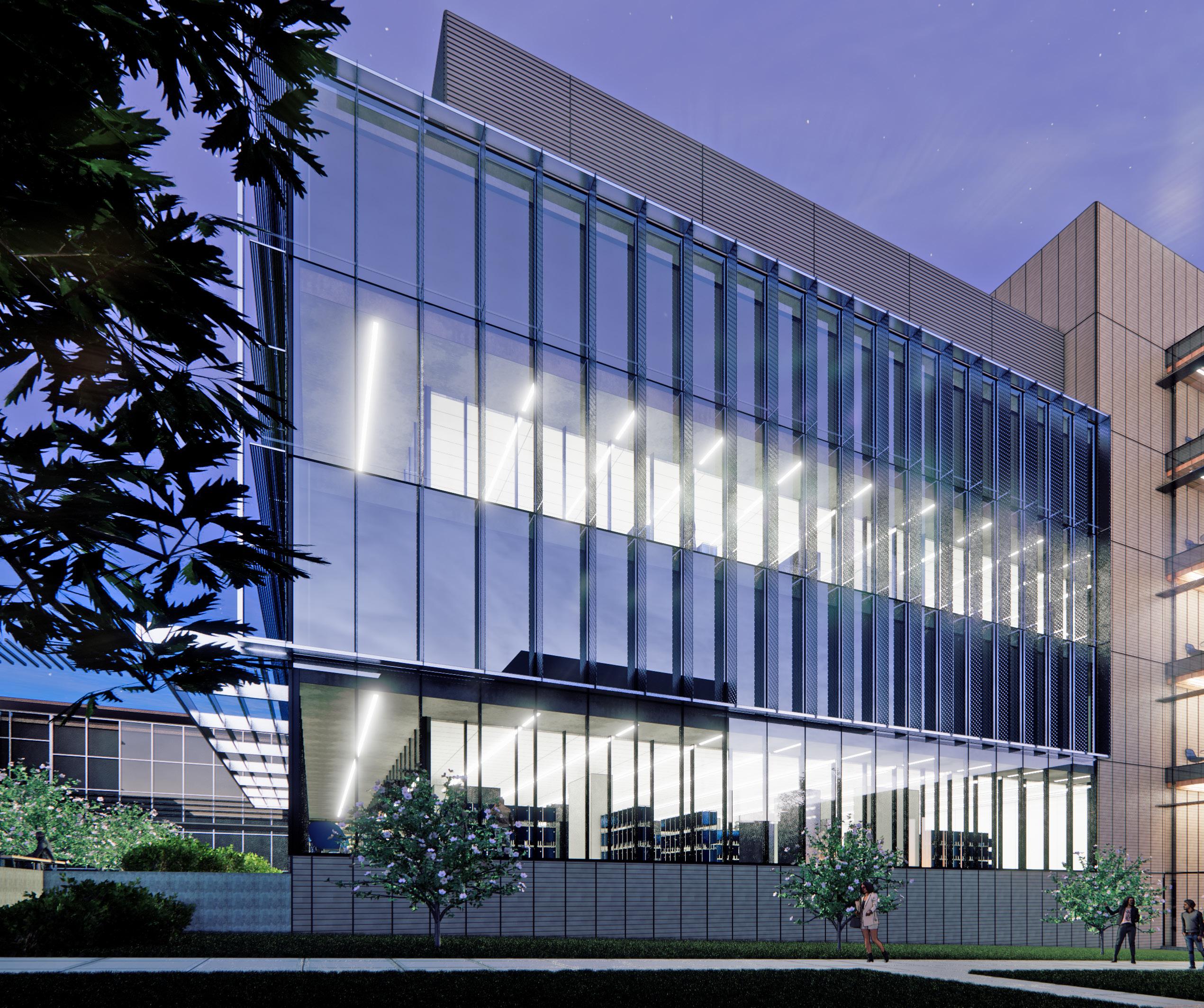
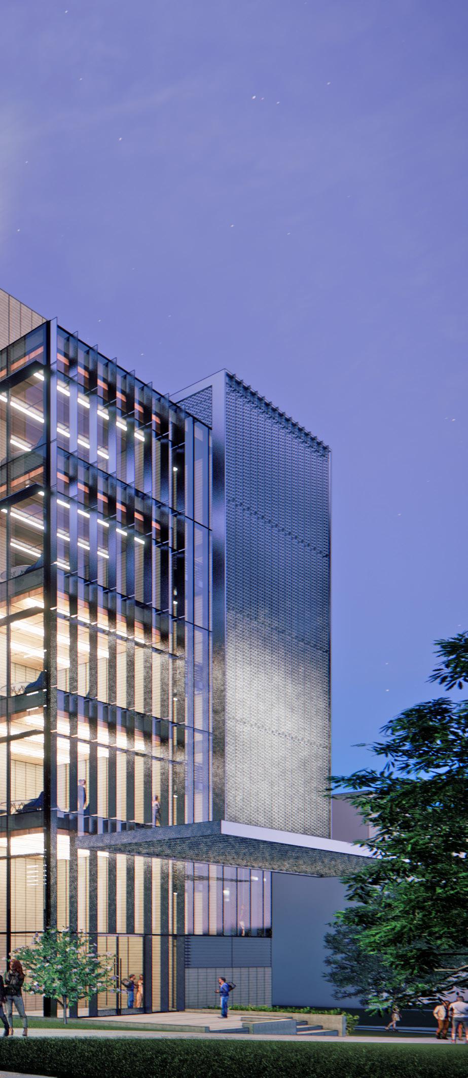
University of Texas at Austin Montopolis Research Campus
For nearly four decades, the University of Texas at Austin Cockrell School of Engineering and the Texas Institute for Electronics (TIE) Montopolis Research Center have been at the forefront of industry collaboration, hosting leading partners such as Sematech. Today, the historic facility is evolving to meet the demands of next-generation semiconductor research and production.
Our cleanroom renovation pushes performance to new heights, transforming existing fabrication spaces into ISO 4 (Class 10) and ISO 5 (Class 100) environments. With a focus on process optimization, key infrastructure upgrades include Acid Waste Neutralization, Hydrogen Fluoride Waste Treatment, Ultra-Pure Water production, Gas and Chemical Distribution, Supervisory Control and Data Acquisition (SCADA), and Toxic Gas Monitoring Systems (TGMS), Building Automation System (BAS), Clean Air Handling, and HVAC. These enhancements create a world-class research ecosystem designed for flexibility, scalability, and seamless took transitions.
This state-of-the-art fabrication facility—known as the Fab— will serve as a vital hub for the Texas Institute for Electronics (TIE), a powerhouse public-private partnership uniting the State of Texas, top semiconductor and defense electronics firms, national labs, and 13 academic institutions. This initiative restores leading-edge semiconductor manufacturing to U.S. soil, strengthens the supply chain, safeguards national security, and cultivates the next generation of industry pioneers.
Purpose-built to accelerate breakthroughs in semiconductor research and development (R&D) and 2.5D/3D semiconductor packaging, the project followed a fast-track delivery process. The reenvisioned Fab is equipped with the critical infrastructure needed to fuel discovery, innovation, and global leadership in advanced electronics.
Services Provided
Project Management / Architecture / Interior Design / Process Engineering / Lab Planning / Fire Protection / Mechanical Engineering / Electrical Engineering
Relevancies
R&D / Cleanroom / Specialty Chemicals / Bulk Gas / Ultrapure Water / SCADA / Toxic Gas Monitoring (TGMS) / Semiconductor Packaging
Institute of Matter & Systems MicroFUSE
Enabling Project
Services Provided Architecture / Structural Engineering / MEP Engineering / Process Engineering / Construction Management Selection Support
Relevancies
Higher Education / Semiconductor / Research & Development (R&D)
Size
3,400 SF Renovation / Retrofit
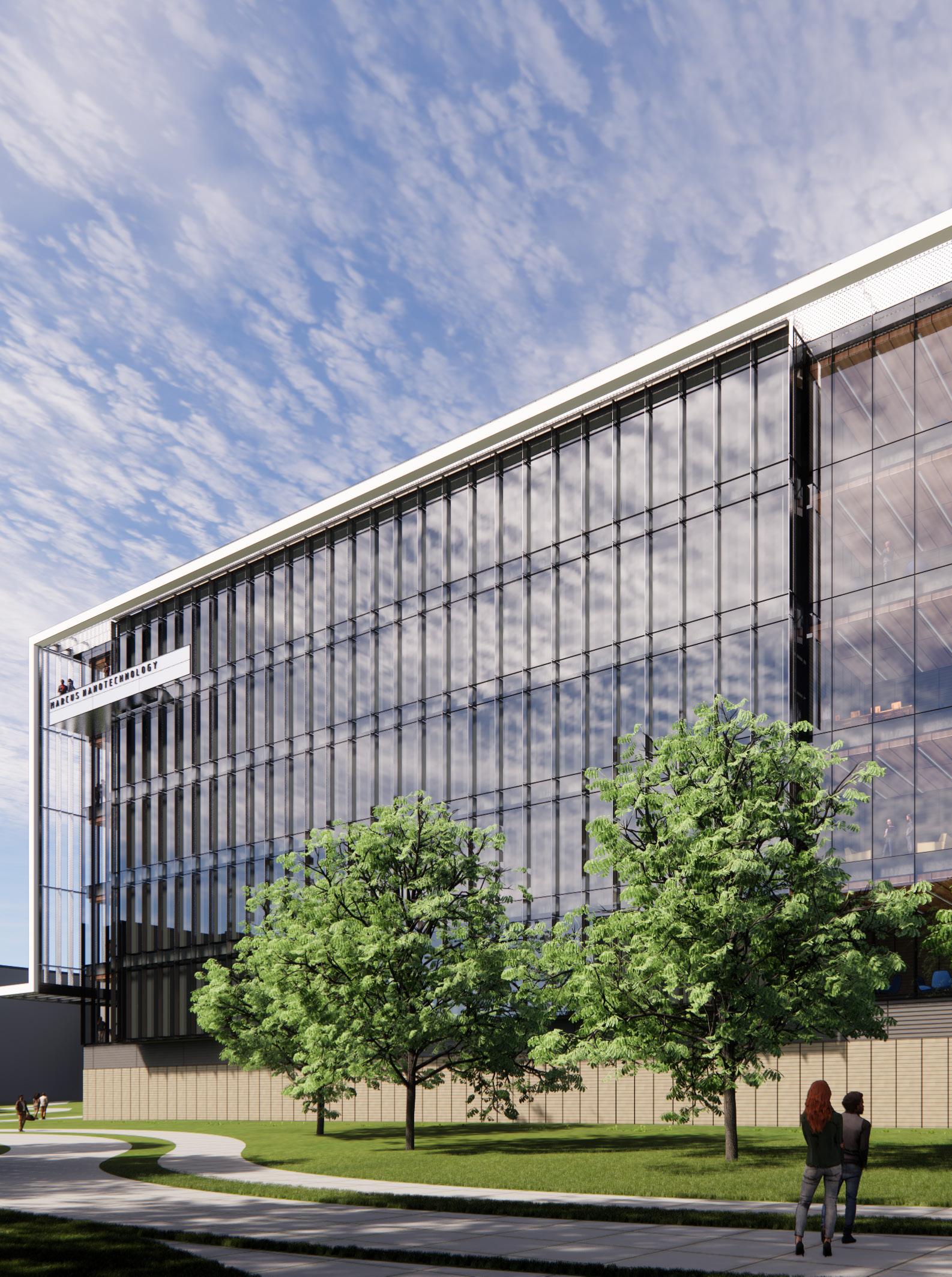
Selected through a competitive process, our firm is leading the expansion of the Marcus Building’s inorganic cleanroom for the Institute of Matter and Systems. The challenge? A precisiondriven 1,500-square-foot ISO 5 cleanroom fit-out seamlessly integrated with the existing ballroom-style cleanroom through a dedicated Move-In/Move-Out path. With a bay-and-chase configuration designed to optimize laminar flow, the space meets rigorous cleanroom certification standards—despite structural constraints imposed by the contiguous slab.
Our design embraces adaptability, ensuring Georgia Tech’s research-driven program can evolve without interruption. A strategic utility delivery system allows for seamless tool reconfigurations, eliminating reliance on external contractors and minimizing downtime.
Playing a critical role in selecting the construction management (CM) team, we ensured the project is executed with the precision and expertise required for a world-class, high-performance cleanroom environment.
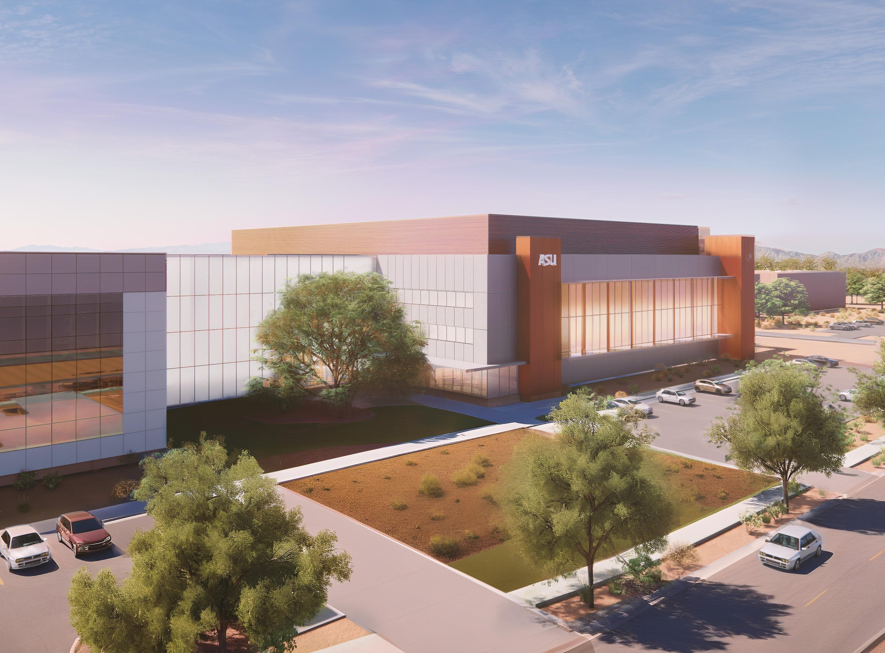
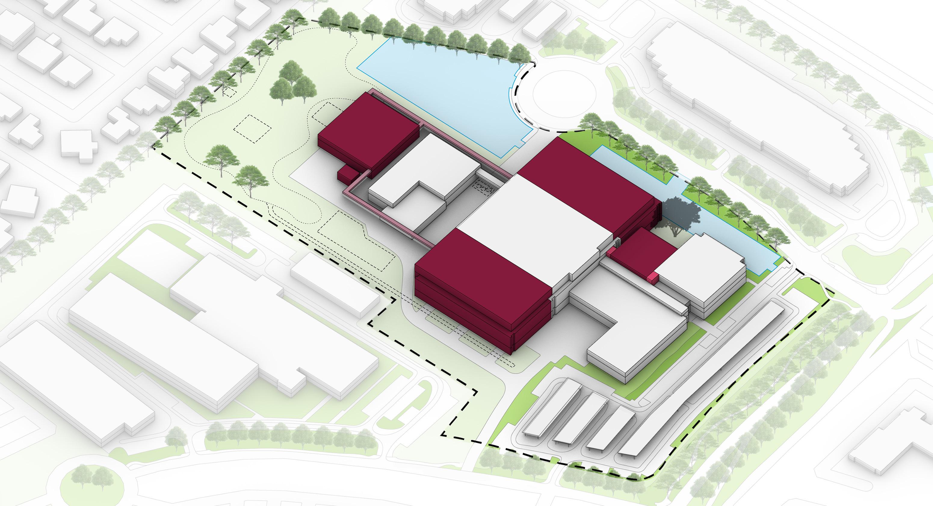
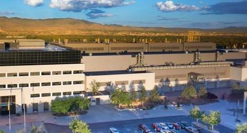
Arizona State University MacroTechnology Works
Originally built in 1997 by Motorola, MacroTechnology Works (MTW) is a 261,188 GSF specialized research and fabrication facility at the center of Arizona State University’s Research Park. Supported by a 26,608 GSF Central Utility Building, the site totals 287,796 GSF. MTW is more than infrastructure; it is a world-class hub that delivers research and fabrication capabilities on a scale unmatched by any other university. It creates direct pathways for ASU to engage industry and drive recruitment, innovation, and national research leadership.
As part of this Facility Master Plan, ASU and the planning team analyzed every aspect of MTW, including infrastructure, users, tools, and active projects, while engaging stakeholders to uncover opportunities to maximize utilization and performance. At the same time, expansion scenarios were tested to push the boundaries of what the site could achieve. The focus was clear: expand fabrication space on the north and south sides of the existing building to maximize cleanroom capacity and reinforce MTW’s role as a singular resource within ASU and beyond.
The result is ambitious. The plan identifies up to 224,400 GSF of new capacity, nearly doubling the site’s total footprint and almost tripling cleanroom space. Designed with flexibility, the expansion can be executed in one bold move or phased strategically over time. Either path positions MTW to scale as a powerful engine for discovery, innovation, and global impact.
Services Provided
Campus Planning / Architecture / Interiors / Engineering / Programming / Lab Planning Assessment / Planning / Infrastructure Planning
Relevancies
Master Planning / Fab / Cleanroom / Central Utility Building / Research & Development (R&D)
Manufacturing
Continental Structural Plastics Manufacturing & Office
Continental Structural Plastics (CSP) is reshaping the automotive and transportation industries with a leading-edge facility dedicated to lightweight composite manufacturing. Strategically located in Seguin, Texas, the facility provides direct access to key clients like Toyota while tapping into a skilled local workforce—strengthened by partnerships with colleges and trade schools.
To bring their vision to life, CSP partnered with us for architecture, engineering, project management, and structural design, ensuring every element was built for performance, scalability, and future industry demands. The result: a 209,653-square-foot facility engineered for growth in the automotive and heavy truck markets.
With seamless collaboration between CSP, our team, and project partners, this facility is a launchpad for innovation, workforce development, and industry leadership.
Grand Prairie, Texas
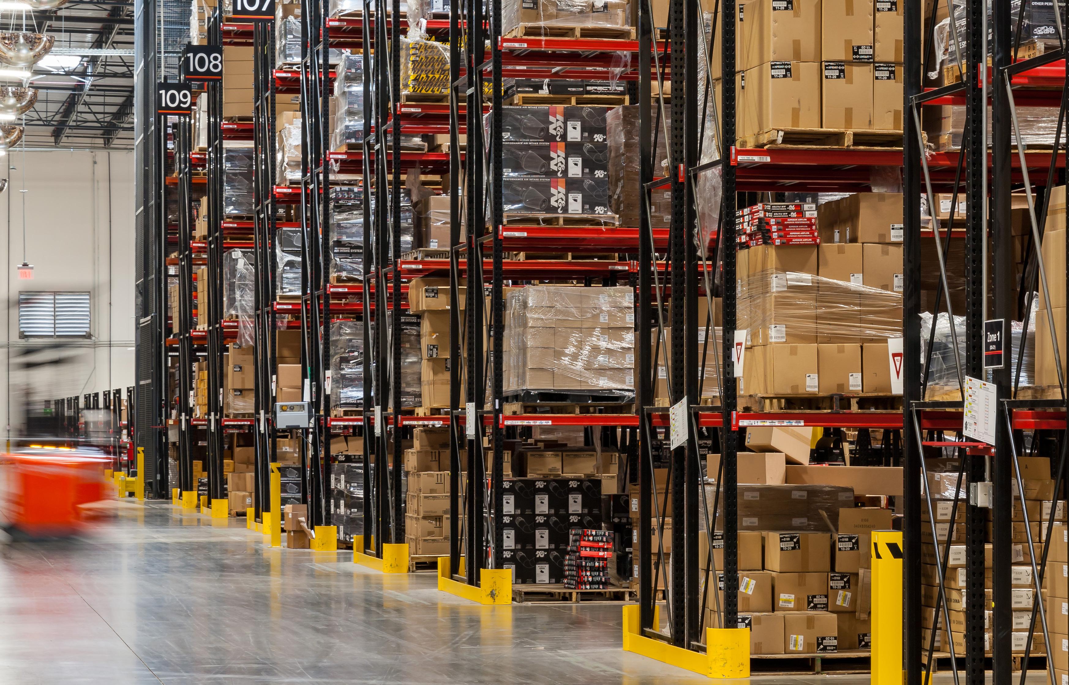
K&N Engineering
New Headquarters & Manufacturing Facility
K&N’s new 30,000-SF office in Grand Prairie, Texas, is built for performance—just like their industry. Inspired by the pleats and conical shape of their filters and the fast-paced world of racing, the showroom, boardroom, and main lobby feature pleated fixtures, wooden beams, and exposed ceilings accented with rock concrete and burnished metal. Everything from the training and break rooms to the warehouse equipment embraces a branded color palette. Houdini glass adds a unique touch, providing layering and depth to the space while protecting R&D areas.
Alongside this striking workplace, our engineers designed a 525,000-SF manufacturing and distribution hub, engineered for efficiency and future growth. The buildings are equipped with the latest technology in manufacturing and distribution equipment, dust-collection systems, and compressed air and nitrogen distribution setups. The team also orchestrated the relocation of a prep and paint production line and designed a floor-supported utility distribution system, ensuring seamless scalability for years to come.
Together, our team and K&N develop cost-effective solutions to their unique manufacturing process needs while offering a best-in-class workplace, creating a high-performing, next-gen environment for 300+ employees.
Services Provided
Architecture / Interiors / Structural Engineering / Mechanical Engineering / Electrical Engineering / Plumbing Engineering / Low Voltage Engineering
Relevancies
Automotive / Auto Parts / Manufacturing / Office / Warehouse / Headquarters / Workplace Design
Size
521,828 SF New Construction
21,367 SF Office Space
500,461 SF Manufacturing Floor and Warehouse
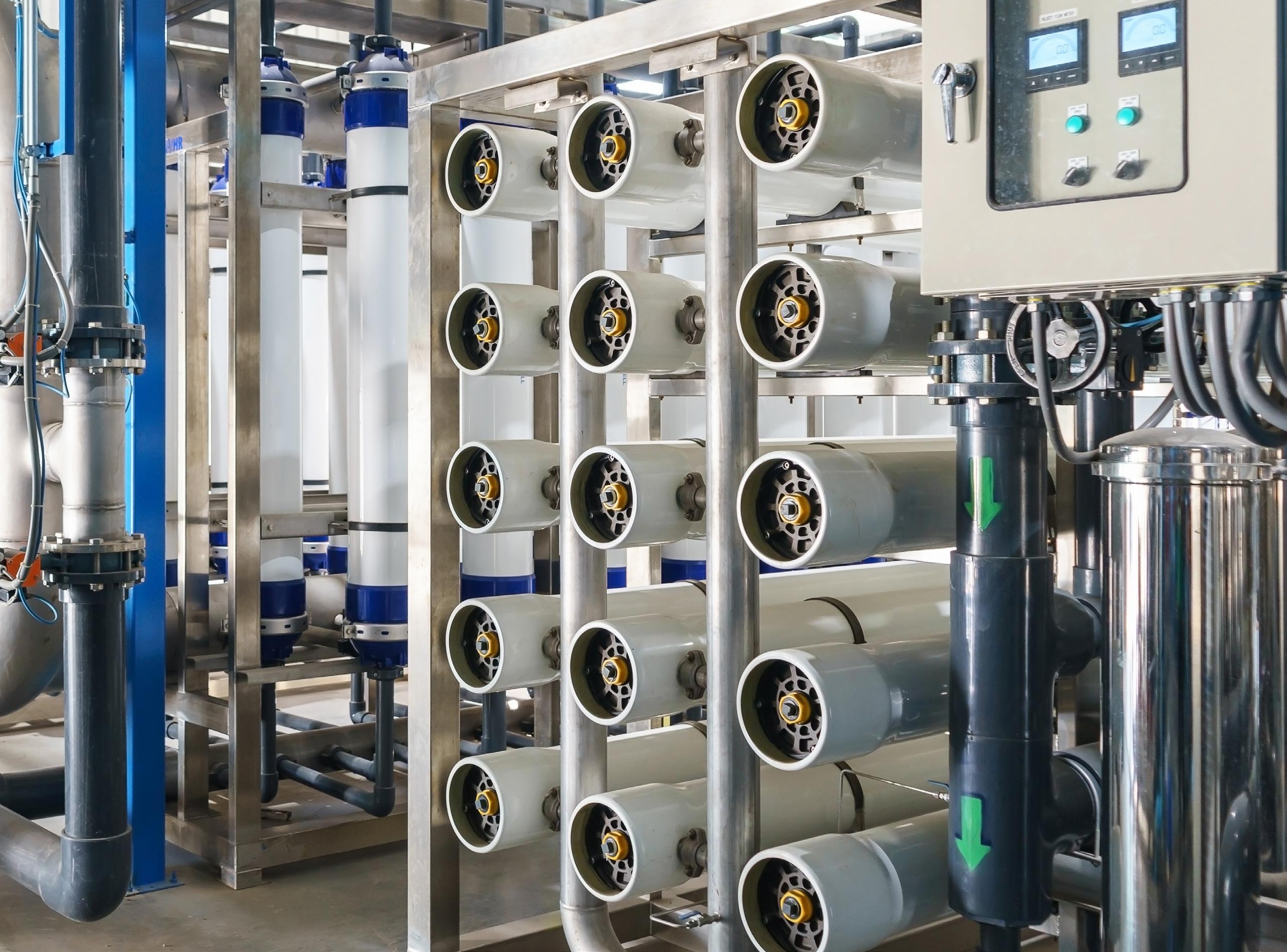
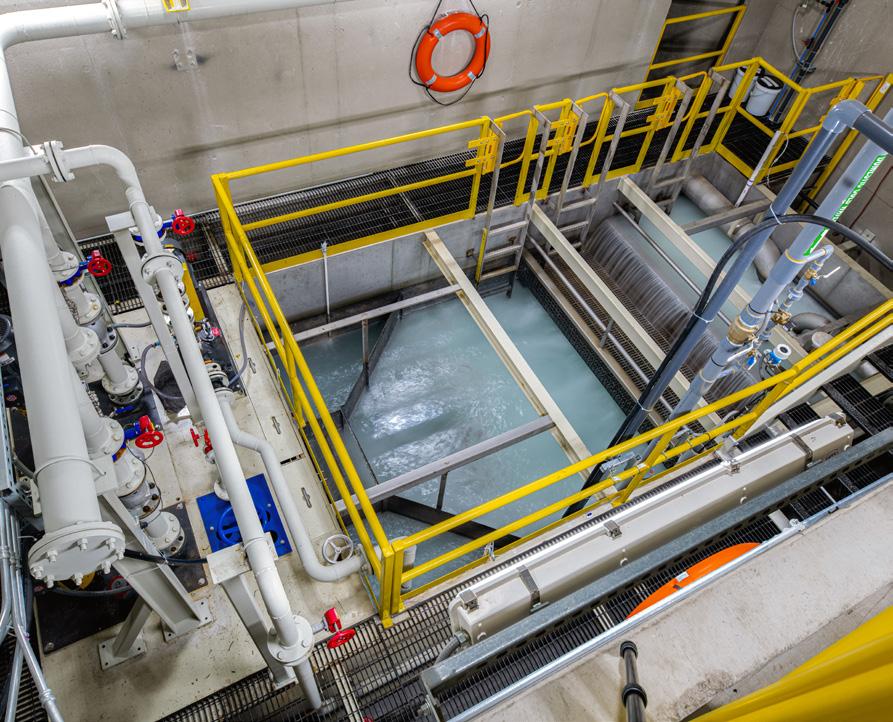
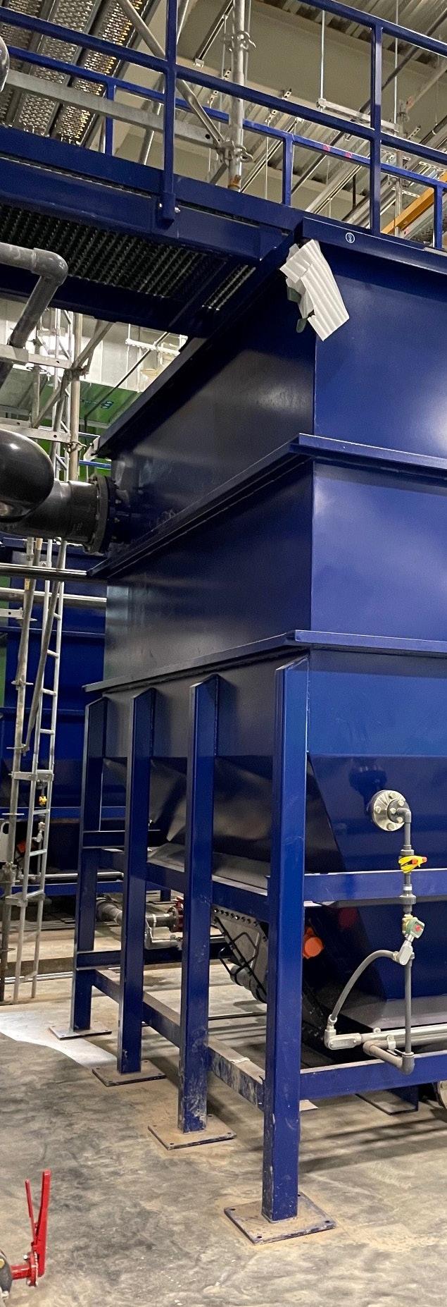
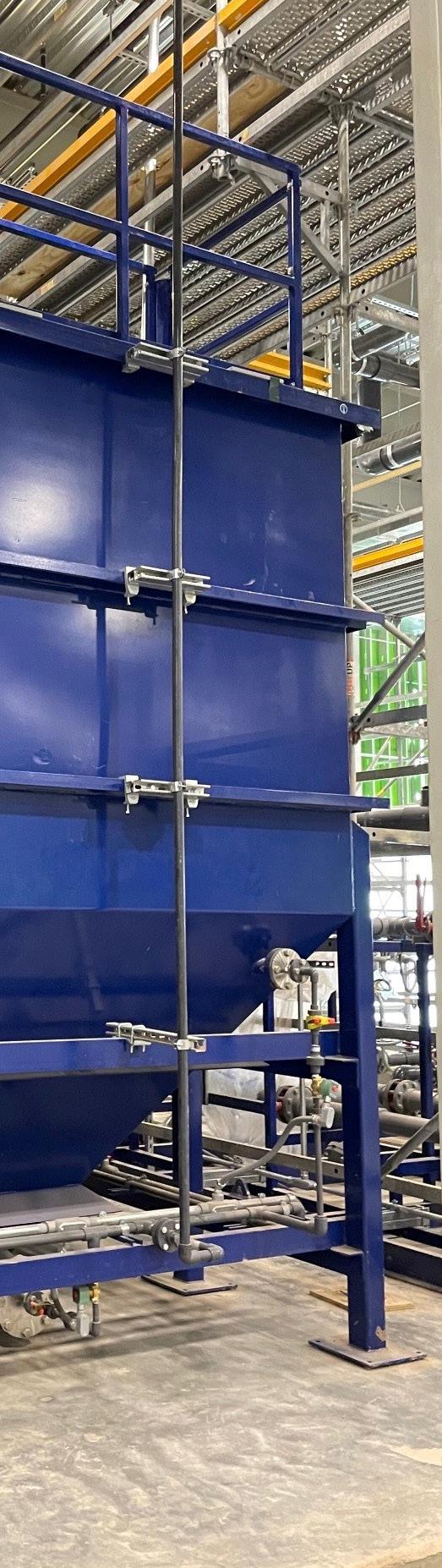
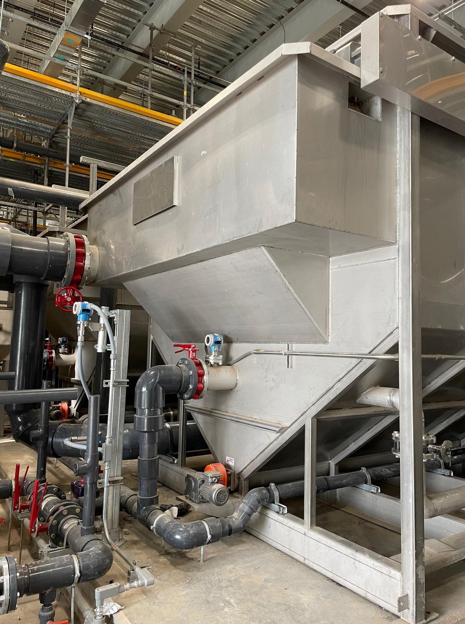
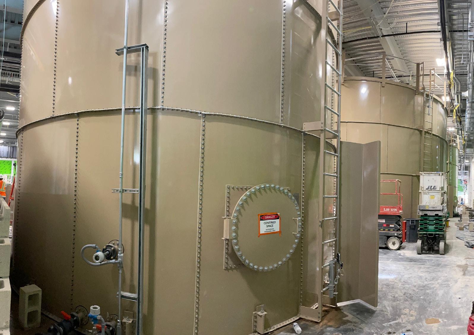
Confidential Electric Vehicle Manufacturer Water / Wastewater System
The Wastewater Design Philosophy used to develop this wastewater system for a confidential electric vehicle manufacturer was based on the process flow established by the process and engineering teams. This selection and arrangement of proprietary modular unit process steps was carefully chosen to maintain proper quality and reliability of the process wastewater system performance, with a focus of giving the customer flexibility for routine maintenance and future expansion without major capital expansion.
The main function of the Wastewater Treatment is to sequester and remove contaminants from each of the manufacturing process lines to achieve levels that consistently meet site discharge levels as prescribed by local compliance requirements from the Basis of Design document for the whole project.
Services Provided
Mechanical Engineering / Electrical Engineering / Plumbing Engineering / Process Engineering
Relevancies
Water-Wastewater Treatment
gal/min
York
Riverbend
Services Provided
Master Planning / Programming / Architecture / Engineering / Project Management
Relevancies
Solar / Manufacturing / Innovation Hub / Central Utility Building / Substation / Warehouse / Office / Locker Room / Training Room / Cafeteria
Size
1,400,000 SF
SUNY Polytechnic Institute, in collaboration with a leading EV manufacturer, is revolutionizing high-tech manufacturing with a state-of-the-art 1.4-million-square-foot solar panel facility— the largest in the northern hemisphere. This one-gigawatt (GW) manufacturing hub stems from the manufacturer’s strategic acquisition of SolarCity, a pioneer in high-efficiency solar technology.
Designed for 24/7/365 operations, the facility supports wafer manufacturing, solar substrate production, and modular assembly—all backed by a new central utility building and campus substation. A 60,000-square-foot shipping
and receiving warehouse optimizes material flow, while a 25,000-square-foot engineering operations office enhances workforce efficiency with locker rooms, training spaces, and a cafeteria—supporting a 1,400-person, two-shift workforce.
From concept to completion, we collaborated with SUNY Poly, the manufacturer, and the development team, driving innovation through comprehensive planning, design, and engineering. This facility is a catalyst for sustainable energy, workforce development, and industry transformation— setting a new benchmark for scalable, high-performance solar manufacturing.
Carson City, Nevada
Confidential Battery Manufacturer BMC1 CAM2 Cathode Active Material Facility
A Confidential Battery Manufacturer is building one of North America’s largest battery recycling and material manufacturing hubs—a 175-acre campus designed to redefine the industry. As part of this transformation, the CAM2 project includes a new three-story, 105-foot-tall, 340,000-square-foot facility dedicated to Cathode Active Material (CAM) production. Applying Performance by Design principles, we ensured seamless operations by optimizing material flow, logistics, and utilities.
To bring this vision to life, the team provided staff augmentation engineering and design expertise, driving the development of high-performance industrial spaces. Key contributions included:
Architectural shell and interiors
HVAC systems for production and cleanroom environments
Process gas infrastructure, including Oxygen and CarbonFree Air
Low- and medium-voltage electrical systems
Instrumentation and controls infrastructure design
The project was strategically phased into design packages for efficiency:
Cold Core & Shell – Structural foundations, architectural shell, and primary steel framework
Basebuild Scope – Architectural detailing, life safety, MEP distribution, and structural support for utilities
Tool Install – Precision-designed utility connections for CAM production equipment
With an innovative, phased approach, this facility is built for efficiency and leading-edge recycling and material manufacturing—a key step toward a more sustainable energy future.
Services Provided
Project Management / Architecture / Interior Design / Mechanical Engineering / Electrical Engineering / Process Engineering / Instrumentation & Controls
Relevancies
Battery / Battery Recycling / Manufacturing / Process Gas / Low Voltage / Tool Install
Rachel Romero Associate Principal /
Jonathan
Sylvie PhD, PE, PMP, FHR Chief Revenue Officer jsylvie@pagethink.com

People experience design long before they recognize it. In the calm of a recovery room. In the hum of the laboratory. In the ease of navigating a campus or a concourse. That doesn’t happen by chance.
As Stantec and Page come together, we offer more than rigor or reach. We are committed to Performance by Design, where every solution is crafted to be purposeful, measurable, impactful. It’s how we turn insights into action, and design into results that move you and your business forward.
Services
Architecture / Engineering / Interior Design / Urban Design / Planning / Landscape Architecture / Branding & Experiential Graphic Design
Markets
Academic / Advanced Manufacturing / Arts & Culture / Aviation / Civic / Commercial & Mixed-Use / Government / Healthcare / Mission Critical / Science & Technology