4 Mapping of Regional Players
Saxony 238
Piemonte 191
Catalonia 189
Bavaria 188
Overijssel 178
Andalusia 89
Thuringia 86
Baden-Württemberg 76
Hessen 65
Helsinki-Uusimaa 52
South Moravia 48
Tampere 43
North Brabant 41
Total: 1,730 entities
The Czech semiconductor ecosystem has a strong regional dimension. Relevant capabilities are distributed across several interconnected regional nodes rather than concentrated in a single location. These include South Moravia, the Zlín Region, Prague, the Plzeň Region, the Ústí Region and other emerging areas of semiconductor competence.
This regional mapping builds partly on activities undertaken in the context of the European
Aim: to map & scope the regional players to identify gaps and interregional collaboration opportunities.
Mapping of regional players led by CSC in cooperation with CNSC, South Moravian and Zlín region for ESRA, May 2026 [9].
Semiconductor Regions Alliance (ESRA). Its purpose is to identify key regional players, characterise existing capabilities, highlight gaps in regional ecosystems and explore opportunities for cooperation between Czech and European regions. It also connects semiconductor development with regional innovation strategies, research and technology infrastructure, industrial specialisation, talent pipelines and investment priorities.
The organisations included in this first edition were selected using a pragmatic and partnership-oriented approach. The mapping primarily covers entities that:
› are demonstrably active in the semiconductor value chain or its supporting ecosystem;
› have been identified through national or regional value-chain mapping activities;
› participate in the Czech National Semiconductor Cluster, the Czech Semiconductor Centre, CzechInvest, ESRA or related cooperation structures; or
› represent potential partners, service providers, users or contributors to future CSC activities.
The mapped organisations include industrial companies, specialised SMEs, fabless and chip-design actors, equipment and metrology suppliers, research organisations, universities, regional innovation centres, public-sector institutions and emerging start-ups. Particular attention is given to highly specialised organisations whose capabilities may be well known within their respective markets but remain less visible across the wider national and European semiconductor ecosystem.
The mapping is intended to support practical cooperation. It can be used to identify suitable partners for research and innovation projects, technology development, investment, training, technology transfer, supply-chain development and interregional initiatives. It will also provide a basis for further engagement with regional stakeholders and for assessing where additional capabilities, services or links to European infrastructure may be needed.
This first edition represents an initial overview rather than an exhaustive regional map. The portfolio of organisations will be expanded and updated as new actors engage with the Czech Semiconductor Centre and the Czech National Semiconductor Cluster, as regional mapping activities progress and as new opportunities emerge under European semiconductor initiatives.
A further update is planned for the calendar year 2027. It will incorporate additional organisations, reflect changes in existing profiles and further strengthen the catalogue’s role as a practical interface between regional Czech capabilities and national and European cooperation opportunities.
[1] MINISTRY OF INDUSTRY AND TRADE OF THE CZECH REPUBLIC. National Semiconductor Strategy [online]. Prague: Ministry of Industry and Trade of the Czech Republic, 2024 [cit. 2026-07-02]. Available from: National Semiconductor Strategy public PDF. https://www.dataplan.info/img_ upload/7bdb1584e3b8a53d337518d988763f8d/ national-semiconductor-strategy-cz.pdf
[2] EUROPEAN COMMISSION. European Chips Act [online]. Brussels: European Commission, DirectorateGeneral for Communications Networks, Content and Technology [cit. 2026-07-02]. Available from: European Chips Act policy page. https://digital-strategy.ec.europa.eu/en/policies/ european-chips-act
[3] CZECHINVEST. Semiconductor Industry in Czechia [online]. Prague: CzechInvest, 2025 [cit. 2026-07-02].
Available from: CzechInvest semiconductor industry profile.
https://czechinvest.gov.cz/getattachment/6fba496dbbd2-4daf-af7e-e8aaedd1a44a/SemiconductorIndustry-in-Czechia-2025
[4] STATISTA. Semiconductors – Worldwide: Market Forecast [online]. Hamburg: Statista [cit. 2026-07-02].
[5] OECD POLICY PAPER. Mapping the semiconductor value chain [online]. Published 2025-06-24 [cit. 202607-07]. Available from: https://www.oecd.org/en/publications/mapping-thesemiconductor-value-chain_4154cdbf-en.html
[6] CZECH NATIONAL SEMICONDUCTOR CLUSTER: https://www.semicz.cz/ with EU Semiconductor Radar: https://smarterinstruments.github.io/Radar/
[7] CZECHINVEST; HAVLÍN, BRIAN; HOLICKÁ, ZUZANA; BLAŽEK, JIŘÍ Value Chain Analysis in the Semiconductor Industry. CzechInvest / Supply Chain Resilience Center, Faculty of Science, Charles University, 2025.
https://czechsemiconductorcentre.cz/czechinvestpublished-a-key-analysis-of-czechias-role-in-thesemiconductor-value-chain/
[8] CEIAS. EU Chips Ecosystem Tracker. Developed as part of the CHIPDIPLO — Chips Diplomacy Support Initiative, 2026.
Tracker: https://chipdiplo.ceias.eu/industry-ecosystem; Information page: https://ceias.eu/chips-diplomacysupport-initiative-chipdiplo/
Available from: Statista worldwide semiconductor market forecast.
[9] EUROPEAN SEMICONDUCTOR REGIONS ALLIANCE / N-ABLE MAPPING MATERIAL (JUNE 2026): https://www.esra-org.eu/#top References
https://www.statista.com/outlook/tmo/ semiconductors/worldwide
This fall 2026, Czech Semiconductor Centre is launching its training and micro-credentials programs.
Rapid Prototyping of Electronic Devices
Rapid prototyping of electronic devices from initial design to functional prototype
Sensors and Actuators Design, Microfabrication, and Packaging
Design, microfabrication, and packaging of advanced sensors and actuators for industrial and research applications
Sensor Design, Fabrication and Calibration
Comprehensive sensor development from design through manufacturing to calibration and validation
Integrated Circuits Analog and Digital Design
Design of analog and digital integrated circuits, including methodologies, simulations, and optimization
You can find the complete list of services and other micro-credentials on our website:
Testing of Analog Integrated Circuits
Testing, measurement, and diagnostics of analog integrated circuits using modern tools
Surface Analysis and Diagnostics of Nanostructures
Surface analysis and diagnostics of nanostructures using advanced methods
www.czechsemiconductorcentre.cz/services
Are you interested in a training course that isn’t listed here? Please provide us with feedback using this questionnaire:
Activair is a technology company focused on the supply and service of vacuum pumps, compressors, blowers, vacuum components and scientific instruments, including AFM, Ellipsometers, Lasers and Spectrometers. We provide expert consulting, technical solutions, design and calculations, equipment delivery, service and support for industrial, research and advanced technology applications.
Contacts
Activair Hillova 1562/15a, 746 01, Opava
www.activair.cz
Mobile number +420 776 793 732
E-mail martin.papula@activair.cz
Competences & Capabilities
Activair offers strong expertise in vacuum technology, blowers, compressed air, gas handling and advanced scientific instrumentation. We provide complete vacuum solutions, including technical consulting, equipment selection and sizing, vacuum and pressure calculations, system design, integration, PLC control, electrical cabinet design and manufacturing, commissioning, diagnostics, preventive maintenance and full service support.
Our competences cover vacuum pumps, compressors, blowers, vacuum components, gauges, sensors, valves, filters, fittings, control elements and complete system assemblies. We offer service capabilities for vacuum pumps, compressors and related technologies, including inspections, repairs, spare parts, troubleshooting and long-term customer support.
Activair also supports customers in advanced research and technology applications. Our portfolio and capabilities include Atomic Force Microscopy (AFM), Ellipsometry, plasma systems, lasers, laser spectrometers, spectroscopy-related devices and other scientific instruments. We provide system integration, technical support, supplier coordination, installation assistance and after-sales service for industrial, laboratory, university, research and advanced technology customers.
Through practical engineering know-how, local service capacity and cooperation with technology partners, Activair helps customers design, integrate, operate and maintain reliable solutions for demanding industrial and scientific applications.
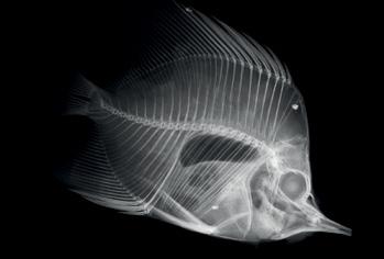
ADVACAM designs and produces cameras for material analysis, non-destructive testing, color radiography, or radiation safety. The technology senses every single particle of radiation of almost any kind, including X-rays, gamma, electrons, ions, and even neutrons. Based on CERN technology, ADVACAM‘s cameras revolutionise a range of industries, from space to medicine. The company provides the ability to image the unseen.
Contacts
ADVACAM s.r.o.
U Pergamenky 12 17000 Praha 7
www.advacam.cz
Mobile number +420 725 594 403 E-mail Vit.Kopelent@advisiones.com
Competences & Capabilities
ADVACAM develops and manufactures advanced radiation imaging and particle tracking systems based on hybrid pixel detector technology. The company combines semiconductor detector expertise with proprietary electronics, firmware, software, and system integration to deliver high-performance photon-counting imaging solutions capable of detecting individual particles of X-rays, gamma rays, electrons, ions, and neutrons. Its noiseless detectors provide simultaneous spatial, temporal, and energy information for every detected particle, enabling spectral imaging and precise radiation analysis.
ADVACAM technologies are deployed in some of the world‘s most demanding scientific and industrial applications. In space, the company‘s compact, low-power detectors operate aboard the International Space Station, NASA‘s Artemis programme, the Gateway Lunar Station, and multiple satellites, where they support radiation monitoring, space weather research, and astronaut protection through particle identification, energy measurement, and directional analysis.
In industrial inspection, photon-counting X-ray cameras enable high-resolution non-destructive testing of advanced materials and manufactured components by revealing internal defects such as porosity, fibre orientation, cracks, and delaminations. The company‘s detector technology also powers compact, high-speed X-ray diffraction and crystallography instruments, enabling significantly faster material characterisation than conventional systems.
Beyond industrial and scientific applications, ADVACAM contributes to biomedical research, including cancer research, biomechanics, and drug development, where energy-resolved X-ray imaging enables improved tissue differentiation and enhanced contrast agent detection. The company also develops tailor-made detector systems and complete imaging solutions designed to meet specific customer requirements, from custom hardware configurations and software integration to application-specific system optimisation.
Allegro MicroSystems (NASDAQ:ALGM) is a global semiconductor leader in sensor and power ICs. We develop intelligent solutions that enable safer, more sustainable technologies while giving customers a competitive edge. If you drive a car, if you use cloud data services (or anything based on Datacentres), if you receive a package delivery, you benefit from our technology.
Contacts
Allegro MicroSystems
Europe Ltd. o.z. Rohanské nábřeží 693/10, Praha 8, 186 00
www.allegromicro.com/en
E-mail gfragiacomo@allegromicro.com
Competences & Capabilities
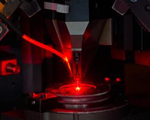
Argotech a.s. (Trutnov, Czech Republic) is an independent European OSAT (Outsourced Semiconductor Assembly and Test) provider specialising in wafer back-end manufacturing, custom packaging, and R&D for semiconductor photonics, microelectronics, and advanced packaging. Operating as a “One-Stop House”, it covers the entire hardware chain from 3D engineering simulations to commercial volume production. Argotech maintains a pure-play service model, providing packaging solutions without developing its own product lines.
With over 1,000 m² of certified ISO 7 and ISO 8 cleanrooms, its core competencies centre on high-precision automated sub-micron die-attach (±1 μm precision) and multi-material wafer-level packaging (WLP). Its automated line processes wafers up to 8 inches, using silicon, alumina, and fused silica substrates. The facility executes eutectic bonding, automated epoxy dispensing, wafer dicing, and die sorting. Argotech special-
ises also in hybrid integration of Photonic Integrated Circuits (PICs) across InP, SiN, and Thin-Film Lithium Niobate (LN) platforms, alongside TO-CAN and butterfly packaging.
The company excels in complex fibre-to-chip coupling—including fibre array butt coupling and lensed fibre alignment—with multispectral capability from ultraviolet to mid-infrared (200 nm to 20 μm). For high-reliability sectors like aerospace, biomedicine, automotive LiDAR, and telecom, Argotech ensures robust hermetic sealing and electro-optical burn-in testing. Backed by 3D simulation for thermal, optical, and RF modelling up to 110+ GHz, Argotech accelerates the entire development lifecycle (EVS-DVS-PVS) from prototyping to high-yield commercial manufacturing.
Analog Bits is a leading semiconductor IP company specialising in ultra-lowpower mixed-signal solutions for advanced SoC design. In 2024, the company expanded into Prague, establishing a dedicated engineering centre focused on next-generation 2nm technologies. The Prague team plays a key role in developing precision clocking, sensing and interconnect IP that enables the most advanced chips in the world.
Contacts
Analog Bits Inc., o.z. Sokolovská 651/136a, Karlín, 186 00 Prague 8
www.analogbits.com
Mobile number +420 602 842 810
E-mail info@analogbits.com
Competences & Capabilities
Analog Bits is a globally recognised semiconductor IP company delivering high-performance, ultra-low-power mixed-signal building blocks that sit at the very heart of modern system-on-chip design. For more than three decades, the company has been developing precision clocking architectures, sensing solutions, and advanced interconnect IP used across computing, automotive, AI, aerospace, and communication systems.
At its core, Analog Bits focuses on enabling silicon to operate reliably at the most advanced process nodes, where power, performance, and physical limits converge. Its portfolio includes PLLs, oscillators, sensors, power integrity monitors, and high-speed interconnect technologies, all engineered to integrate seamlessly into complex SoC environments.
A significant milestone in the company’s evolution came in 2024 with the establishment of its engineering design centre in Prague. This expansion marked a strategic move
into Europe’s growing deep-tech ecosystem and created a focused hub for advanced semiconductor development. The Prague team has rapidly become an important contributor to cutting-edge research and development, particularly in technologies targeting 3nm and the emerging 2nm generation of semiconductor processes.
This Prague-based engineering group is deeply involved in next-generation IP development, helping to push the boundaries of what is physically possible in modern chip design. Working close to the limits of silicon scaling, the team focuses on ensuring stability, power efficiency, and reliability in environments where traditional design assumptions no longer apply.
By combining global expertise with local engineering talent, Analog Bits continues to strengthen its position as a critical enabler of next-generation semiconductor innovation, bridging the gap between physical silicon constraints and the demands of future computing systems.
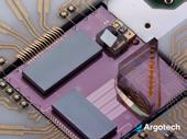
Argotech a.s. (Trutnov, Czech Republic) is an independent European OSAT provider specialising in wafer back-end manufacturing, custom packaging, and R&D for semiconductor photonics. Operating as a „One-Stop House“, it covers the chain from simulations to high-volume production in ISO 7/8 cleanrooms. It offers sub-micron die-attach (±1 μm precision), WLP up to 8“, PIC integration, fibre coupling, thermal modeling and RF modelling up to 110+ GHz. Company experience 20+ years in photonics.
Contacts
Argotech
Holubova 978, 547 01
Náchod
www.argotech.cz
E-mail argotech@argotech.cz Mobile number +420 739 203 013
Competences & Capabilities
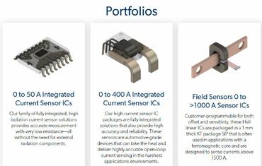
The Allegro MicroSystems Prague Centre of Excellence specializes in the design, verification, and implementation of advanced current sensor ICs using Allegro’s high-voltage BCD process technologies. Core expertise includes analog and digital design, system engineering and mixed-signal design verification (MSDV), ensuring robust, high-quality semiconductor solutions that meet stringent automotive functional safety standards, including ISO 26262 and ASIL compliance. The stateof-the-art Prague laboratory provides comprehensive characterization, validation, and customer support, serving as a key technical partner for global Field Application Engineers (FAEs) and customer designs.
Products & Services
In collaboration with global teams, the Prague Centre of Excellence develops high-performance magnetic current sensor ICs across three core technologies: integrated conductor, field (coreless), and Tunnel Magnetoresistance (TMR) sensors.
Key products include the ACS37002, a high-bandwidth Hall-effect current sensor with fast overcurrent detection and configurable analog output, and the ACS37601, a programmable Hall-effect field current sensor supporting functional safety up to ASIL-C. The team is also advancing TMR sensor technology to deliver exceptional sensitivity, thermal stability, and ultra-low noise.
These solutions replace traditional shunt-resistor approaches by integrating high-voltage isolation, thermal management, and programmable overcurrent protection, improving efficiency, simplifying system design, and enhancing safety in 400V and 800V industrial and e-mobility applications. The Prague team also provides advanced simulations, evaluation boards, and design support to accelerate customer development worldwide.
ASICentrum, established in 1992, is a design centre of EM Microelectronic, belonging to the Swatch Group. EM is a semiconductor manufacturer specialized in the design and production of ultra-low power, low voltage integrated circuits for battery-operated and field-powered applications across consumer and automotive industries. It includes Bluetooth LE controllers, the sensors for IoT devices, the broad portfolio of RFID devices.
Contacts
ASICentrum Novodvorská 994, 142 00, Prague 4
www.asicentrum.com
Mobile number +420 226 772 111 E-mail info@asicentrum.cz
Competences & Capabilities
ASICentrum design capabilities include the complete flow starting by specification definition with the customer and ending by qualification a device for mass production.
The design expertise is focused on hybrid analog/digital devices with ultra low power management, unique analog circuitry (sensors, RFID front-end, oscillators), MCU systems based either with standard CPU like RISC-V/ARC, or proprietary company CPUs.
Main product families are:
• LF, HF and UHR RFID devices included dual-mode (HF&UHF)
• Sensors for IoT devices: optical, temperature, pressure, acceleration, magnetic, touch
• Bluetooth LE controllers
• Timing circuits (oscillators, RTC, watch processors)
• Energy harvesting controllers
• Power management circuits (watchdog, supply supervisory)
Profiles of companies
EM Microelectronic offers the following services:
• design and manufacturing of standard devices
• design and manufacturing of ASICs
• design and manufacturing of automotive devices
• design and manufacturing of electronic modules (e.g. BLE beacons)
• semiconductor fab in Switzerland
• IC testing
BeamShape is a deep-tech electron-beam company founded in 2023 in Brno — a global hub of electron microscopy. We design and build proprietary electron-optical systems: the foundational technology behind semiconductor inspection, metrology, e-beam lithography and advanced manufacturing. Our team combines deep scientific expertise with proven commercial and technical leadership from the world‘s leading electron microscopy companies.
Contacts
BeamShape Purkyňova 649/127, Brno-Medlánky, 612 00
www.beamshape.com
E-mail info@beamshape.com Mobile number +420 775 249 720
Competences & Capabilities
Drawing on Brno’s specialised e-beam supplier ecosystem and a broad network of world-class scientific collaborators, we develop custom electron-optical components and provide R&D services to OEM partners building and advancing electron-beam instruments. Our work ranges from precision lens and deflection systems and electron-optical sub-assemblies to complete electron-optical modules, helping partners improve resolution, stability and beam control. We work under NDA with instrument manufacturers and research institutions globally, supplying precision components at specifications that match or exceed industry benchmarks.
Products & Services
EOD (Electron Optical Design) - BeamShape is the exclusive global distributor of this industry-standard simulation suite, used by leading electron-microscope manufacturers and research institutions worldwide to design and optimise complete electron columns - from source to sample - including aberration analysis and
mechanical tolerancing. BeamShape provides licences, technical training and dedicated support to clients across Europe, North America and Asia.
EBMelt — BeamShape’s own high-power electron-optical column for advanced electron-beam manufacturing, capable of processing demanding high-temperature and refractory metals such as tungsten and titanium that other approaches handle poorly.
Codasip is a Czech-founded semiconductor company developing RISC-V processors and silicon solutions that are secure by design. At the core is CHERI — a breakthrough architecture that embeds fine-grained memory protection directly into hardware, eliminating vulnerability classes underpinning 70% of cyber threats. Founded in 2014, Codasip is a founding member of RISC-V International. Codasip — Resilient by Design.
Contacts
Codasip Šumavská 416/15, 602 00 Brno, Czechia
www.codasip.com
Phone number: +420 519 810 190 E-mail info@codasip.com
Competences & Capabilities
Codasip is a Czech-founded semiconductor company building the foundation of the next era of secure computing. As cyber threats grow in scale and sophistication, the industry is undergoing a fundamental shift: security can no longer be added after the fact — it must be embedded at the architectural level.
Codasip exists to enable this transformation. The company develops RISC V-based processors and silicon solutions that are secure by design, helping customers worldwide create systems that are inherently resilient rather than reactively protected.
At the core of Codasip’s approach is its integration of CHERI (Capability Hardware Enhanced RISC Instructions), a breakthrough architecture developed in collaboration with the University of Cambridge, DARPA and SRI International. By embedding fine-grained memory protection directly into hardware, CHERI eliminates entire classes of vulnerabilities, including
Profiles of companies
memory corruption and buffer overflow attacks that underpin a 70% of today’s cyber threats.
Complementing the portfolio of RISC-V CPU cores (Embedded to Out-Of-Order HPC) is Codasip Studio, the company’s processor design automation platform. Studio enables rapid customisation, verification, and toolchain generation for RISC V processors, allowing both Codasip and its customers to efficiently develop differentiated, application-specific designs while maintaining strong security guarantees.
Building on its heritage in processor IP, Codasip evolved in 2026 into a full-stack semiconductor company, bringing secure RISC V silicon to market. Founded in 2014 in the Czech with locations globally, Codasip is a founding member of RISC V International and represents European deep-tech innovation shaping the future of hardware-enforced security on a global scale.
Codasip — Resilient by Design
Crytur is a first-class European provider of integrated optoelectronic solutions for science and high-tech industry. It is the world’s leading supplier of detection units for electron microscopy used for semiconductor wafer characterisation and inspection, Europe’s largest supplier of laser rods, a key supplier of materials for particle physics, and a specialist in complex optomechanical assemblies and laser solutions.
Contacts
Crytur
Na Lukách 2283, 511 01
Turnov
www.crytur.com
E-mail sales@crytur.cz
Mobile number +420 481 319 511
Competences & Capabilities
The key to Crytur’s long-term success lies in coherent material application and proprietary R&D in cooperation with leading universities and scientific institutes, resulting in a wide variety of crystal-based radiation detectors as well as new materials. This approach has made Crytur the world’s leading supplier of scintillation detectors for electron microscopy and the largest European supplier of laser rods.
Nowadays, Crytur shifts towards the development and production of more complex solutions, such as detection units with precise mechanical parts, complex laser sources, high-power light sources or radiation detection systems.
Two large manufacturing facilities located in Turnov enable Crytur to operate all key technologies on site together with a top-quality controlling process (ISO 9001) and semiconductor-level clean room assembly.
Our broad portfolio targeting diverse markets such as Semiconductors, Particle Physics, Medical & Beauty, Defence and others, includes:
• Crystal and semiconductor-based detectors for electron microscopy and wafer inspection, and other customised opto-electronic and opto-mechanical solutions.
• Laser rods, active laser materials and laser modules for lasers, laser micromachining, UV lithography and spectroscopy.
• Precise optical and mechanical (metal, ceramic) parts and modules.
• High-power light sources.
• Scintillation crystals and crystal-based radiation detectors and systems for high-energy physics, imaging, laboratory equipment, geological prospecting and sorting.
DynaNIC is a university spin-off delivering FPGA-based SmartNIC acceleration for high-speed networks. Built on proprietary FPGA firmware, the platform combines hardware-level performance with software-like adaptability. It enables terabit-scale packet processing without in-house FPGA expertise. Core use cases include DDoS mitigation, 5G UPF, deep packet inspection, and lawful interception.
Contacts
DynaNIC Semiconductors
Božetěchova 1/2, Královo Pole, 612 00 Brno
dyna-nic.com
Phone number: +420 773 477 946 E-mail info@dyna-nic.com
Competences & Capabilities
• Digital Chip Design & RTL Engineering: High-end digital design expertise focusing on programmable silicon and high-performance FPGAs. We specialize in developing energy-efficient, ultra-low latency network pipelines operating at line rate from 100G to 400G and beyond.
• Advanced Hardware Verification: Robust verification pipelines ensuring the absolute reliability of complex digital designs. We leverage state-of-the-art simulation, functional verification, and hardware-in-the-loop emulation to deliver production-ready, zero-packet-loss architectures.
• Academic Roots & Deep R&D: Originating as a university spin-off from FIT VUT Brno, our team combines deep academic research in programmable hardware with extensive industry experience in FPGA firmware engineering and high-performance packet processing.
Products & Services
• FPGA-Based Software Acceleration Platform: A turnkey platform that abstracts the complexity of digital chip and FPGA development through standard DPDK and RTE Flow interfaces. It enables network and security teams to deploy hardware acceleration without needing specialized in-house RTL or silicon expertise.
• Production-Ready Network IP Cores: High-performance, vendor-agnostic IP blocks optimized for critical use cases, including line-rate DDoS mitigation, 5G UPF offload, deep packet inspection (DPI), lawful interception, and advanced telemetry.
• SmartNIC Integration & Lifecycle Extension: Deployment services and firmware solutions across AI, telco, cloud, and cybersecurity infrastructure. We support multi-vendor SmartNICs, offering broad hardware flexibility while reducing both CAPEX and OPEX by upgrading existing capabilities without hardware replacement.
Profiles of companies
Edhouse. For over 20 years, we have helped customers deliver complex technology projects – from analysis and design through development to testing and long-term support. Our expertise spans industrial software, embedded systems, automation, AI, cloud solutions, DevOps, cybersecurity and UX/UI.
Contacts
Edhouse
Vavrečkova 7074, 760 01 Zlín
www.edhouse.eu
E-mail sales@edhouse.cz Mobile number +420 799 020 355
Competences & Capabilities
We develop software and hardware solutions for technology-driven industries where reliability, precision and long product lifecycles are essential. Our multidisciplinary teams combine software engineering, embedded development, systems engineering, Quality Assurance, AI, cloud technologies, DevOps and cybersecurity to support complex engineering projects.
Quality is built into every stage of development. Through test automation, verification and continuous quality assurance, we help customers minimise risk, improve software reliability and accelerate product delivery.
Products & Services
Our engineers support the development of industrial software, embedded systems, production support applications and engineering tools. We integrate software with manufacturing equipment, enterprise systems and cloud platforms, enabling efficient data
exchange, process automation and better operational visibility.
We help customers apply AI to solve real engineering challenges, including process optimisation, anomaly detection, intelligent automation and data analysis. At the same time, we design scalable cloud architectures and integrate cybersecurity into the entire software development lifecycle.
One example is our contribution to software for electron microscopes and other scientific instruments, where precision, stability and rigorous software testing directly influence the quality of the final product. These same engineering principles enable us to support customers across the semiconductor ecosystem and other high-tech industries.
Edwards. With more than 100 years of vacuum engineering expertise and a global presence across Europe, Asia and North America, Edwards supports the technologies behind the chips powering AI, healthcare, mobility and the digital economy. Combining European heritage with a global customer base, we help shape the future of semiconductor manufacturing through innovation, insight and partnership.
Contacts
Edwards
Spielberk Office Centre
Holandská 10 639 00 Brno
www.edwardsvacuum.com
Phone number: +420 533 44 1045
E-mail Sales_EMEA@edwardsvacuum.com
Competences & Capabilities
From Europe to the world’s most advanced semiconductor hubs, Edwards helps create the environments where innovation thrives.
The Czech Republic plays an important role in Edwards’ global operations. In Brno, Edwards operates a major remanufacturing centre for dry vacuum pumps, supporting customers across Europe, including many of the continent’s leading semiconductor manufacturers. In Lutín, our teams focus on the research, development and manufacture of scientific vacuum pumps used in research and high-technology applications worldwide.
At the heart of every semiconductor fabrication facility lies vacuum technology. From deposition and etch processes to advanced packaging, highly controlled vacuum environments are essential to manufacturing modern semiconductor devices. Edwards develops vacuum, exhaust management and abatement technologies that help manufacturers achieve the precision,
reliability and process control required for increasingly complex technology nodes.
Our technologies support semiconductor manufacturers across the globe, from Europe’s innovation centres to many of the world’s most advanced fabs in Asia and North America. Through these collaborations, Edwards brings together expertise and best practices from across the global semiconductor ecosystem, helping customers improve productivity, reduce environmental impact and advance sustainability goals.
Founded in the United Kingdom in 1919 and now part of the Atlas Copco Group, Edwards combines engineering heritage with global scale. Whether supporting AI infrastructure, advanced memory, power semiconductors or future process technologies, our purpose remains the same: creating the environments where innovation thrives.
EP Rožnov, a.s. was founded in 1992 and is focused on comprehensive design and construction of cleanrooms, particularly in industrial sectors involving semiconductor manufacturing, automotive components, aerospace, optics as well as research and development. Cleanroom design and implementation include a complete architectural and construction solution, including building technical systems.
Contacts
EP Rožnov, a.s.
Boženy Němcové 1720, 756 61 Rožnov pod Radhoštěm
www.eproznov.cz
E-mail ep@eproznov.cz
Mobile number +420 702 287 456
Competences & Capabilities
Our specialty is the comprehensive design in the BIM system and construction of cleanrooms, particularly in industrial sectors and research and development.
Our cleanroom design and implementation include a complete architectural and construction solution, including building technical systems such as HVAC, cooling, heating, electrical systems, instrumentation and control systems, process media piping and other utility systems.
We process the project documentation in the BIM system. More than 50 of our experienced professional designers work in individual teams to prepare project documentation.
Each cleanroom has its specific requirements and our goal is to find an optimal solution for operating and capital costs while achieving maximum energy efficiency in cleanrooms. The subsidiary company Epigon provides the development, production, and assembly of components for cleanroom installations, with a focus on customized customer solutions and offer complete deliveries and assemblies of process media piping.
Thanks to our many years of experience, we are able to
plan and implement the construction of cleanrooms in parallel with existing production with minimal restrictions and impact on its operation. We carry out qualification measurements and validation of cleanrooms.
Products & Services
Complex cleanroom solution
BIM project documentation
• Development of feasibility studies
• Processing of a complete project documentation in the BIM system
Cleanroom installation
• Construction implementation and management
• Bespoke supplies of cleanrooms
• Commissioning and trial operation
• Warranty and post-warranty service
Qualification measurement and validation
• Installation Qualification
• Operational Qualification
• Process Qualification
We create cleanrooms for those creating the future.
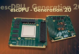
esc Aerospace is a European SME focused on space-qualified hardware and software for space and defense. The company develops mission-critical software, on-board systems (OBC, DPU), secure communications (QKD, SATCOM), and payloads like radiation sensors, hyperspectral cameras or LiDAR. ESC also works in UAV/C-UAS, supports Czech space missions, and develops its own hyperspectral satellite with secure connectivity.
Contacts
esc Aerospace
Čs. armády 14 160 00 Prague 6
www.esc-aerospace.com
Phone number: +420 604 347 014 or +420 284 683 784
E-mail richard.sysala@esc-aerospace.com
Competences & Capabilities
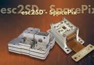
esc2SD: Spacepix – Dosimetry System
A unique Space Dosimetry System built for CubeSat platforms with a proven flight heritage from the VZLUSAT-2 satellite launched in 2022. The system features a powerful data processing unit based on a 32-bit ARM processor, which controls two independent detectors and processes the acquired data.
The first detector, a radiation monitor based on the revolutionary SpacePix® ASIC, is designed for space radiation monitoring, including galactic cosmic rays, solar wind, and trapped radiation electrons and protons. It enables particle energy and species determination using pattern recognition and partial trajectory reconstruction. It supports operational modes of radiation imaging, clustering, tracking, and LET histogramming, and includes an alert capability for elevated radiation. The proton detection threshold is 1.5 MeV and electron threshold is 80 keV, with
Profiles of companies
particle identification via hit signature analysis.
The second detector is the SXM (Soft X-Ray Monitor). Based on the XChip03 SXR ASIC, the SXM measures the flux and spectrum of soft X-rays during solar transient events like
X-ray flares. It is sensitive to photons in the energy range of 4 to 20 keV, manages a maximum X-ray flux of 105 photons/cm²s-1, and includes charged particle discrimination. Standard data products include raw frames, X-ray flux, and spectra.
Together, these detectors form a versatile space dosimetry and space weather monitoring system capable of delivering high-resolution radiation data for scientific, commercial, and operational space missions. For more detailed technical specifications, visit our website.
Fyscon s.r.o. is a Czech engineering company specializing in custom precision machinery, advanced mechanical systems, and high-precision engineering solutions for semiconductor, scientific, and advanced industrial applications. With in-house development and manufacturing capabilities, we deliver complete turnkey solutions from concept to commissioning.
Contacts
Fyscon s.r.o. Vavrečkova 5262 760 01 Zlín
www.fyscon.cz
E-mail info@fyscon.cz
Mobile number +420 702 287 456
Competences & Capabilities
Fyscon s.r.o. provides comprehensive engineering services covering the entire product development cycle—from concept design and mechanical engineering to precision manufacturing, assembly, testing, installation, and commissioning. Our multidisciplinary team develops bespoke mechanical systems and automation solutions tailored to each customer’s technical requirements.
Our core competence is custom engineering. Every project is individually designed to solve specific technological challenges while ensuring precision, reliability, and manufacturability. We combine advanced CAD design, structural analysis, technical documentation, precision machining, assembly, and system integration within our own development and production facilities, enabling efficient project execution and full control over quality.
We develop and manufacture high-precision mechan-
ical components, assemblies, and specialized equipment for scientific instrumentation and semiconductor manufacturing technologies, where accuracy, stability, and long-term reliability are critical.
In addition to industrial engineering, Fyscon develops proprietary technologies through its NanoBioTech Division. The division focuses on advanced additive manufacturing systems for the controlled deposition of micro- and nanofibers, supporting research institutions and biomedical innovation.
By combining strong engineering expertise with flexible in-house development and manufacturing capabilities, Fyscon transforms complex technical challenges into fully engineered, production-ready solutions. We serve as a long-term technology partner for customers developing next-generation industrial, scientific, and semiconductor technologies.
Hitachi Energy is a global technology leader in electrification with innovative power grid technologies with digital at the core. With mission-critical technologies like high-voltage, transformers, automation, and power electronics, the company is addressing the most urgent energy challenge of our time –balancing soaring electricity demand, while decarbonizing the power system.
Contacts
Hitachi Energy Czech republic Novodvorská 1768/138a
142 00 Prague 4
hitachienergy.com
Phone number: +420 228 887 700 E-mail salesdesksem@hitachienergy.com
Competences & Capabilities
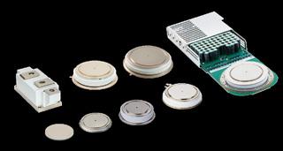
The main competence in the semiconductor ecosystem of Hitachi Energy in the Czech Republic is the front-end production of silicon power discrete devices. This goes hand in hand with the packaging of bipolar power modules, IGCTs, as well as welding, rectifier, and fast recovery diodes. An integral part is the application testing developed within the company to provide the cutting-edge technologies for the sectors like generation and transmission of electrical energy, traction, industry, and automotive.
The manufacturing and R&D facilities of bipolar power semiconductor components operated by Hitachi is a legacy of Czech engineering stemming from former ČKD Semiconductors, later acquired by ABB Semiconductors, which today belongs to Hitachi.
Products and services
Together with Hitachi Energy in Switzerland, we offer one of the most diverse power semiconductor portfolios, including GTOs, IGBTs, IGCTs, Thyristors, and Diodes in
Profiles of companies
the power range of 150 A up to 13500 A and 200 V up to 8500 V. High power semiconductors are key components to control the power generation and connection of the network from renewable energy sources such as wind turbines, photovoltaic cells, and hydro-power plants.
The semiconductors are used for several tasks in the chain of renewable energy sources like the conversion of power in the plant, such as in wind turbines, the transmission of power to the grid, interconnection of separated grids or back-to-back solutions for grid stabilization, the integration of electrical storage options as well as the grid-forming control capability for stable operation in weak grids, and reduction of voltage unbalances. Hitachi Energy is the sole fully vertical integrated provider of high-voltage direct current (HVDC) systems for efficient transmission of electrical energy.
Hitachi Energy Czech republic
H TEST a.s. is specialized technical distributor of test and measurement instruments for semiconductor and electronic components development and production.
Contacts
H TEST
Šafránkova 3
155 00 Prague 5
www.htest.cz
E-mail info@htest.cz
Mobile number +420 235 365 207
Competences & Capabilities
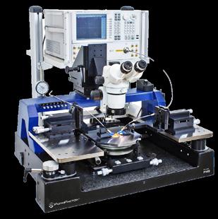
The main competences of H TEST are distribution and system integration of test instrumentation for measurement, evaluation and quality control of semiconductor components. H TEST helps its customers to test and evaluate semiconductor components and structures in both encapsulated and on-wafer formats. We deliver solutions for R&D laboratories as well as for manufacturing lines. We also provide tools and probe stations for reliable connection between test system and device under test.
Products & Services
Our portfolio includes wide spectrum of electronic test instruments for testing, measurement and probing of semiconductor components: source-measurement units (SMU), parametric analyzers, curve-tracers, impedance analyzers, LCR meters, precision multimeters, oscilloscopes, precision power supplies and many others. We also offer test system integration services, consulting and trainings.
Inference Technologies develops production-grade predictive systems for semiconductor manufacturing. Our DeepFab platform transforms design, process, inspection, test, and manufacturing data into actionable insight that helps fabless companies, IDMs, and foundries improve yield, reduce reliability risk, accelerate ramp-up, and make faster data-driven production decisions.
Contacts
Inference Technologies Kačírkova 982/4 Prague 5
www.inferencetech.com
Phone number: +420 702 066 383 E-mail contact@inferencetech.com
Competences & Capabilities
Inference Technologies specializes in predictive systems for semiconductor manufacturing. We develop and deploy production-grade software that converts existing fab-native data into operational intelligence for yield improvement, reliability control, and production optimization.
Our expertise spans wafer fabrication, process integration, defect inspection, electrical test, yield learning, reliability analysis, and AI/ML model development. We work with heterogeneous semiconductor datasets including process data, inspection results, wafer maps, PCM/WAT measurements, electrical test data, burn-in data, and manufacturing records.
Our flagship platform, DeepFab, provides predictive capabilities for:
• Yield learning and yield prediction
• Defect relevance and latent defect screening
• Reliability risk assessment and field-failure reduction
Profiles of companies
• Root-cause analysis and process optimization
• Smart wafer, lot, and die routing decisions
• Production monitoring and decision support
For fabless semiconductor companies, DeepFab helps bridge the gap between design teams and manufacturing partners by providing data-driven insight into yield loss mechanisms, reliability risks, and foundry performance. For IDMs and foundries, DeepFab enables earlier detection of process excursions, yield-impacting factors, and reliability issues before they propagate into production losses or field failures.
All solutions are designed to integrate with existing customer infrastructure and operate within secure customer environments. Our engagement models range from feasibility studies and pilot projects to long-term deployment of predictive manufacturing systems.
Korymbos Photonics is a university spin-off developing advanced semiconductor metrology tools using terahertz light. Its technology enables fast, precise, and contactless measurement of material properties like thickness and doping, improving yield and quality in a broad semiconductor industry, including SiC and GaN for high-power applications.
Contacts
Korymbos Photonics
17. listopadu 2172/15 708 00 Ostrava-Poruba
korymbos.com
E-mail info@korymbos.com
Mobile number +420 723 159 635
Competences & Capabilities
Korymbos Photonics provides advanced metrology solutions for the semiconductor industry, enabling precise, fast, and non-destructive material characterisation. The company’s core innovation is based on terahertz (THz) ellipsometry, a cutting-edge optical technique that bridges electronics and photonics to deliver highly accurate insights into semiconductor structures.
Its primary offering is an inline, contactless measurement tool designed for high volume manufacturing. The system enables real time monitoring of key parameters such as layer thickness, doping concentration, and material properties across the full wafer stack. With rapid, single-shot measurements and a stable, high-speed architecture, it significantly improves process control, production yield, and overall device quality.
Korymbos Photonics also offers measurement services, providing customers with high-quality analytical data
without the need for capital investment. This approach delivers a cost-effective alternative to traditional destructive techniques, while enabling faster turnaround and richer datasets for process evaluation and optimization.
In addition, the company develops specialized systems for R&D, including compact ellipsometry kits and nearline tools tailored for process tuning and experimental validation. These solutions support industrial teams, universities, and technology developers.
Korymbos Photonics serves the full semiconductor ecosystem, covering both established and emerging materials such as silicon (Si), gallium arsenide (GaAs), indium phosphide (InP), silicon carbide (SiC), and gallium nitride (GaN). By combining deep scientific expertise with strong industry alignment, the company addresses the growing demand for reliable metrology in next-generation electronics, power devices, and advanced computing applications.
Leadec is a global service specialist for industrial environments, supporting the entire lifecycle of factories. With over 60 years of experience, 22,500 employees and more than 350 locations in 16 countries, the company delivers tailored solutions that enhance efficiency, quality and sustainability in manufacturing industries.
Contacts
Leadec Českobratrské náměstí 1392
Mladá Boleslav, 293 01
www.leadec-services.com
E-mail info-czech@leadec-services.com
Competences & Capabilities
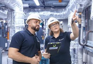
With a strong global presence and extensive industry experience, Leadec delivers high-performance solutions for the semiconductor and microelectronics sectors. The company operates in highly controlled environments where precision, cleanliness, and reliability are essential. Its strength lies in combining deep technical expertise with modern digital solutions such as IoT platforms, advanced data analytics, and process optimization tools. This approach supports predictive maintenance, improves transparency, and drives continuous operational improvement. Working in line with international standards, including ISO 9001, ISO 14001, and ISO 45001, Leadec consistently meets the highest requirements for quality, safety, and sustainability while helping customers increase efficiency and move toward their decarbonization targets.
Products & Services
Leadec offers an integrated portfolio of technical and infrastructural services tailored to complex manufacturing environments. These include facility management, maintenance of critical utility systems, cleanroom services, machine installation and relocation, as well as technical cleaning and quality inspections. Designed to maximize uptime and operational efficiency, all services are delivered with a strong focus on reliability and performance. As a trusted long-term partner to leading global manufacturers, Leadec supports customers throughout the entire factory lifecycle, driving sustainable productivity and operational excellence.
Profiles of companies
Leadec
Mycroft Mind is a software and data science company developing self-learning AI/ML algorithms for energy grid devices. Our specialisation is embedded energy intelligence – predictive algorithms engineered to run on resource-constrained microcontrollers without cloud dependency, within the memory and compute budgets of hardware already in the field: smart meters, PV inverters, EV chargers, substation RTUs and data concentrators.
Contacts
Mycroft Mind Šumavská 416/15
602 00 Brno
www.mycroftmind.com
E-mail info@mycroftmind.com
Mobile number +420 511 112 170
Competences & Capabilities
Our expertise sits at the intersection of machine learning, embedded software engineering and energy systems, covering the full signal chain from raw sensor input to structured operational outputs. Algorithms adapt autonomously on-device, learning from local data. Embedded intelligence modules are portable across chipset architectures, making integration into device makers’ pipelines straightforward.
On low-voltage grids, we map topology, identify phase connections, localise losses and model demand, generation, flexibility and EV charging, translating outputs into autonomous or operator-supervised control using existing infrastructure.
Products & Services
Our portfolio currently covers five solution areas:
Grid Intelligence – substation load controllers, EV charging grid management and observability tools that raise hosting capacity, deployable on existing RTUs and edge controllers.
Metering Intelligence – embedded detection of arc faults, consumption anomalies and PLC quality, running on the meter’s existing MCU without additional hardware.
Photovoltaic Intelligence – SkyEye, a short-term PV forecasting system combining sky-image processing with meteorological data.
Energy Market Intelligence – day-ahead demand and generation forecasting for flexibility operators, aggregators and traders.
Meter Data Management – large-scale metering data processing, warehousing and device lifecycle management.
NANOTECHNA s.r.o. is developing polymer-based photonic chips doped with nanoparticles for the next generation of petahertz electronics. Their technology combines better thermal management for higher performance with flexible, stretchable chips attachable to different surfaces.
Contacts
NANOTECHNA
Vojtova 1538/6 Prague 12 - Modřany, 143 00
www.nanotechna.com
E-mail david.ettel@nanotechna.com
Competences & Capabilities
NANOTECHNA´s devices are designed for lower power consumption, higher efficiency at THz repetition rates, and a greener lifecycle solution — with reduced energy demands during production and operation, and easy recyclability. We are developing polymer based chips doped by nanoparticles for Petahertz electronics. NANOTECHNA s.r.o. is paving the way for sustainable, high-performance photonics that integrate seamlessly across diverse applications.
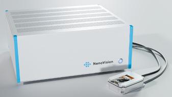
NenoVision s.r.o. is a Brno-based deep-tech company developing LiteScope — an atomic force microscope (AFM) integrated inside a scanning electron microscope (SEM). This AFM-in-SEM approach enables in-situ nanoscale electrical measurements without sample transfer, accelerating semiconductor failure analysis and process control.
Contacts
NenoVision Purkyňova 649/127 612 00 Brno
www.nenovision.com
E-mail info@nenovision.com
Mobile number +420 511 112 170
Competences & Capabilities
NenoVision’s mission is to accelerate nanoscale discovery by bringing correlative AFM-in-SEM analysis directly to where it matters most — inside the electron microscope, at the exact site of interest.
The company specialises in AFM-in-SEM instrumentation for advanced semiconductor failure analysis and process control. Key capabilities include in-situ site-specific electrical characterisation without sample transfer, enabling significantly faster time-to-result. In advanced physical failure analysis, LiteScope enables conductivity mapping at the interconnect level following plasma FIB delayering — a workflow validated in collaboration with leading semiconductor manufacturers. For process control, supported techniques include scanning spreading resistance microscopy (SSRM) for dopant concentration profiling at the transistor level, and thickness measurement of doped epitaxial and implanted layers. Together with Umberto Celano from Arizona State University (ASU), NenoVision also intro-
duced electron-beam-excited cAFM — a novel method enabling back-contact-free electrical characterisation potentially compatible with in-line workflows.
Beyond semiconductors, LiteScope serves a broad range of research fields — including battery and energy materials, 2D materials, metals and alloys, and powders and particles — wherever in-situ nanoscale electrical or mechanical characterisation at a specific site is critical.
NXP Semiconductors is a global leader in secure connectivity and embedded processing solutions serving the automotive, industrial & IoT, mobile and communications infrastructure markets. In the Czech Republic, NXP operates major engineering centres in Rožnov pod Radhoštěm and Brno, contributing to advanced semiconductor, software and system development.
Contacts
NXP Semiconductors
1. máje 1009
756 61 Rožnov pod Radhoštěm
www.nxp.com/company/about-nxp/worldwide-locations/czech-republic:CZECH
E-mail adminczech@nxp.com Mobile number +420 571 665 111
Competences & Capabilities
NXP Semiconductors is a leading semiconductor company headquartered in Eindhoven, the Netherlands, developing secure connectivity and embedded processing solutions for automotive, industrial & IoT, mobile and communications infrastructure applications. The company combines semiconductor, software and system expertise to support the development of connected, secure and intelligent technologies worldwide.
NXP Czech Republic is one of the company’s longstanding engineering locations in Europe. The Rožnov pod Radhoštěm site traces its origins to the Motorola Design Centre established in 1993, with the Motorola Application Lab founded in 1995. The Brno site was established in 2009 and has since become an important software-focused engineering centre.
Today, NXP Czechia is described internally as a strong engineering community with nearly 500 employees across Rožnov, Brno and university-oriented activities in Ostrava
Profiles of companies
and Zlín. The organisation combines research and development, software engineering, validation, customer support and specialised business functions, with a strong emphasis on technical expertise, innovation and long-term capability building.
Czech teams contribute to a broad range of technologies, including automotive software, connectivity, security, embedded systems, artificial intelligence, software validation and next-generation vehicle architectures. The sites also participate in European research and innovation initiatives and support the advancement of semiconductor technologies and software-defined systems.
A key part of NXP Czech Republic’s identity is its cooperation with universities and technical schools. Through internships, student projects, competitions, technical events and academic partnerships, NXP supports the development of future engineering talent and promotes collaboration between industry and academia.
onsemi delivers intelligent power and sensing technologies that enable electrification, energy efficiency, safety, and automation across automotive, industrial, and AI data center end markets. With a highly differentiated and innovative product portfolio, onsemi helps customers solve complex challenges to achieve higher efficiency, improved performance, and lower system cost, while supporting a safer, cleaner, and more energy efficient world.
Contacts
onsemi
1. máje 2634, 756 61, Rožnov pod Radhoštěm
www.onsemi.com
E-mail sekretariat.CZ@onsemi.com
Mobile number +420 605 842 281
Competences & Capabilities
onsemi in the Czech Republic is one of the country’s largest employers in the semiconductor industry and a vital part of the global onsemi manufacturing and design network. Its main site in Rožnov pod Radhoštěm combines high-volume wafer fabrication with the production of raw silicon wafers and epitaxial layers, including silicon carbide (SiC) capabilities. The company also has two design centres in the Czech Republic, one in Rožnov pod Radhoštěm and one in Brno.
onsemi has a long-standing history in the Czech Republic dating back well into the 20th century. Building on the legacy of Tesla Rožnov, whose employees worked in electronics — and later in semiconductors — 70 years ago.
The company has its own research and development facility in the Czech Republic, focusing on semiconductor materials engineering and new product development. Over 300 of onsemi’s international patents originate
from the Czech Republic. onsemi produces 3 billion chips and 3 million silicon and silicon carbide wafers in Rožnov pod Radhoštěm every year.
onsemi’s operations in the Czech Republic cover a broad range of the semiconductor value chain, including silicon and silicon carbide (SiC) wafer production, epitaxy, chip manufacturing, process engineering, product and technology development, IC design, testing, and quality and reliability activities. The company also collaborates with universities and industrial partners. onsemi intends to expand its SiC operations in the Czech Republic to strengthen the European supply chain for advanced power semiconductors.
Pacellico is a management consultancy focused on supply chain transformation and operational excellence for high-tech manufacturing, specialising in the semiconductor industry. Since 2006, the company has supported global clients in improving procurement, planning, manufacturing operations, and end-to-end supply chain performance through data-driven analysis and hands-on delivery.
Contacts
Pacellico Jar. Svobody 235 66447 Střelice
pacellico.com
E-mail mnecas@pacellico.com (Martin Nečas) Mobile number +420 602 210 868
Competences & Capabilities
In the semiconductor industry, Pacellico improves supply chain resilience, visibility, and forecasting accuracy in complex global environments. The focus is on identifying risks, quantifying opportunities, and translating them into financially robust actions that improve margins, working capital efficiency, and sustainable growth. The approach combines supply chain analytics, value stream mapping, and organisational diagnostics to identify performance drivers and design transformation programmes. It integrates quantitative modelling with operational experience to manage volatility in procurement, capacity constraints, and multi-site manufacturing networks. Pacellico has delivered multiple transformation programmes globally, generating over USD 250 million in measurable financial impact. Core expertise includes supply chain strategy, procurement optimisation, demand and capacity planning, inventory reduction, and manufacturing footprint optimisation. Proprietary analytics tools enable rapid processing of
Profiles of companies
complex datasets, scenario modelling, and decision support for root-cause analysis, process mapping, and investment evaluation
Products&Services
Pacellico supports onshoring and offshoring strategies, helping semiconductor subsystem suppliers strengthen precision manufacturing, cleanroom operations, and localised production closer to end markets. Assessments provide a fact-based foundation for decision-making through management interviews, onsite observation, and data analysis, delivering a 360° view of operations with quantified risks, opportunities, and financial impact. Advanced analytics, benchmarking, and value stream mapping identify inefficiencies, define future-state operating models, and translate recommendations into prioritised, financially quantified actions focused on supply chain design, procurement optimisation, customer alignment, and business resilience.
Pacellico
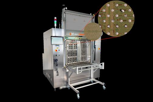
PBT Works s.r.o. is a Czech family-owned company specializing in research, development, and manufacturing of cleaning machines for electronic assemblies. With over 30 years of experience, we focus on cleaning solutions for PCBAs, active and passive component packaging processes, stencils, tooling, and more. Through our extensive distributor network, we maintain a global presence with support centres in key electronics markets worldwide.
Contacts
PBT Works s.r.o.
Lesní 2331 756 61 Rožnov pod Radhoštěm
E-mail info@pbt-works.com
Mobile number +420 602 740 758
Competences & Capabilities
Over the years, PBT Works gained deep expertise in removing soft soldering residues from various assemblies, including components before packaging, chip-scale modules, and power modules.
We mainly use wet cleaning methods, primarily spray-inair technology with specially designed non-flammable engineering liquids. This allows us to solve challenging projects in micro-mechanical and optical applications.
We have also built ultrasonic and spray-under-immersion cleaning systems with high automation for dedicated customer projects.
As the main purpose of electronics cleaning is to increase surface energy and prevent electrochemical corrosion, we have developed strong analytical capabilities for testing and verifying cleanliness. We promote innovative process optimization methods, such as glass models of component packages. These tools help us to study and optimize cleaning results under components.
In addition, we design and implement automation solutions, including robot integration and data sharing for smart factories.
Products and Services
Our core products are cleaning machines for removing flux residues after soldering. Many are also suitable for maintenance cleaning of precision tools and fixtures contaminated with flux, solder paste, thermal materials, coatings, and more.
We also manufacture offline stencil printers for pasty materials, ideal for laboratories, prototyping, and small production.
Thanks to our global distributor and service network, we provide worldwide customer support.
Beyond manufacturing, we offer comprehensive process support. Every cleaning project is unique due to different parts, contamination types, soldering processes, materials, and wastewater requirements; therefore, we assist clients with initial parameter setup and long-term process stability.
Renesas is an embedded semiconductor solution provider driven by its Purpose ‚To Make Our Lives Easier.‘ As the industry’s leading expert in embedded processing, we have evolved to provide scalable and comprehensive semiconductor solutions for automotive, industrial, infrastructure, and IoT industries based on the broadest product portfolio, including High Performance Computing, Embedded Processing, Analog & Connectivity, and Power.
Contacts
Renesas Klicperova 3208/12
150 00 Prague 5
www.renesas.com
E-mail jan.kovalsky.yk@renesas.com Mobile number +420 234 717 700
Competences & Capabilities
Our mission is to develop a safer, healthier, greener, and smarter world by providing intelligence to our four focus growth segments: Automotive, Industrial, Infrastructure, and IoT that are all vital to our daily lives, meaning our products and solutions are embedded everywhere.
Main four segments we operate in:
• Automotive › Highly reliable vehicle control, safe & secure autonomous driving and eco-friendly electric vehicles
• Industrial › Lean, flexible and smart industry
• Infrastructure
• Robust infrastructure, enabling safety and efficiency
• IoT › Comfortable, safe and healthy lifestyles through IoT
Renesas delivers a vast array of semiconductor products, from sensors to actuators, across the whole signal chain to help our customers realize complete embedded systems.
Profiles of companies
• Microcontrollers & Microprocessors
• Analog Products
• ASIC & IP
• Automotive Products
• Clocks & Timing
• Interface
• Memory & Logic
• Power Discretes
• Power Management
• Programmable Logic
• Sensor Products
• Space & Harsh Environment
• Wireless Connectivity
Our proven, comprehensive solutions combine Renesas’ complementary product portfolios of Analog + Power + Embedded Processing + Connectivity. These Winning Combos help our customers and partners around the world accelerate their designs and get to market faster.
Renesas also offers a wide variety of software, boards, simulation & design tools, etc, to make our customers’ lives easier. Also, our certified partners with expertise in Renesas products will support our customers at every stage of the design to achieve their goals. Each partner program also provides opportunities for new business creation.
Renesas
SmarterInstruments Business development and consultancy based on 20+ years of experience in semiconductor industry, generative and ultra low power AI for IoT & energy grid, cooperation with most of semiconductor vendors, embedded systems HW & SW design, IPCEI projects, EU Chips Act, Czech National Semiconductor Strategy, Pilar I. design platform and competence centres network in EU.
Contacts
SmarterInstruments
Lidická 29, Brno, 602 00
smarterinstruments.eu
E-mail cerny@smarterinstruments.eu
Competences & Capabilities
Wide network of partners for projects EU, Taiwan business development from disruptive idea to real partnerships, funding, projects
IPCEI – complete guidance for the process, economics, disruptive technologies funding
EUChipsAct – guidance for utilization of components, fabless design, AI chips
Energy grid &IoT
Ultra low power AI use cases on low power, low performance MCUs platforms
Ecosystem managements, semiconductor value chain partners identification
STMicroelectronics At ST, we are creators and makers of semiconductor technologies. We work with our customers and partners to design and build products, solutions, and ecosystems that address their challenges and opportunities, and the need to support a more sustainable world.
Contacts
STMicroelectronics
Pobřežní 620/3
186 00 Praha 8
www.st.com Mobile number +420 605 74 74 00
Competences & Capabilities
We create semiconductor solutions which are integrated into each of the billions of electronic devices people across the globe interact with every day. By getting more from technology to get more from life, ST stands for life augmented.
We build products, solutions, and ecosystems that enable smarter mobility, more efficient power and energy management, and the wide-scale deployment of cloud-connected autonomous things.
KEY FACTS
• Integrated device manufacturer with 14 main manufacturing sites
• President and CEO: Jean-Marc Chery
• Public since 1994: traded in New York, Paris, and Milan
• Corporate headquarters: Geneva (CH)
• Committed to sustainability: Signatory of the United Nations global compact
• (UNGC), member of the responsible business alliance (RBA)
• Committed to be carbon neutral on scope 1 & 2 and
Profiles of companies
focusing on product transportation, business travel and employee commuting emissions for scope 3 by 2027
SALES & MARKETING
• $11.8B revenue in 2025
• Offices in 40 countries
• Over 200,000 customers worldwide
PEOPLE & INNOVATION
• 49,000 employees worldwide
• ~120 nationalities
• 9,500 people working in R&D and product design
• 20,000 active and pending patents
We create innovative semiconductor solutions based on:
• Dedicated Automotive ICs
• Analog, industrial and Power conversion ICs
• GP MCU & MPU, Wireless solutions, secure MCU, EEPROM
• Discrete and power transistors
• MEMS and optical sensing solutions
• ASICs based on ST proprietary technologies
STREICHER focuses on the custom development and manufacturing of vacuum equipment and systems for leading research institutions, as well as for applications in the space and semiconductor industries. With more than 30 years of experience, it provides expertise, innovation, and reliability as part of the multinational STREICHER Group (DE), together with sister companies operating under the STREICHER Advanced Vacuum brand.
Contacts
STREICHER Plzeňská 565 332 09 Štěnovice
www.streicher-advancedvacuum.com
E-mail sales@streicher-advancedvacuum.com
Competences & Capabilities
We develop and deliver highly customized vacuum and thermal vacuum solutions tailored precisely to our clients’ requirements, covering the entire process from initial development to final on-site assembly.
Our high-precision in-house manufacturing is followed by cleaning, assembly, commissioning, and packaging under cleanroom conditions up to ISO 5, ensuring the highest standards of cleanliness and contamination control required for semiconductor, optical, and UHV applications – including systems up to 50 tons.
The collaboration with STREICHER Maschinenbau and MAX STREICHER Department of Electrical Engineering and Automation under the STREICHER Advanced Vacuum brand enables us to support complex and demanding projects with a strong focus on innovation, quality, and long-term partnership.
We provide vacuum chambers for a wide range of demanding processes, including thin-film deposition,
plasma processing and etching, photonics applications, and other high-tech industrial applications. Our modular thermal vacuum system, S-CUBE TVAC, is designed to simulate controlled thermal environments under vacuum levels down to 1×10⁻⁷ mbar, enabling reliable thermal cycling and testing for aerospace, semiconductor, and high-tech industrial applications.
Our S-UV component cleaning system for UHV and semiconductor applications, based on UV technology, offers significantly faster processing and substantially lower energy consumption compared to conventional thermal bake-out methods. Our expertise in the optical and semiconductor industries is further demonstrated by our status as a “Preferred ZEISS Supplier”.
Products & Services
• Design & development of vacuum systems
• Inhouse manufacturing up to 50 t
• Electrical measurement and control technology
• Assembly & testing up to ISO 5
• On-site installation & service
STROZA s.r.o. is a Czech engineering company specialized in custom automation, robotics, and chemical process equipment for the semiconductor industry. We design complex systems for wet processes, wafer handling, hazardous chemical distribution, and precision inspection. Our tailor-made solutions emphasize process stability, safety, and seamless clean-room integration.
Contacts
STROZA s.r.o.
Bezručova 663, 756 61, Rožnov pod Radhoštěm
www.stroza.cz
E-mail stroza@stroza.cz Mobile number +420 571 752 911
Competences & Capabilities
The core competence of STROZA lies in developing turnkey technological units for chemical processing and high-precision handling in clean-rooms. We possess deep engineering expertise in designing structures from high-performance, chemically resistant plastics that safely withstand aggressive acids and solvents critical to wafer fabrication.
Key capabilities include automating chemical etching, washing, rinsing, and drying sequences, where absolute repeatability, temperature control, and fluid dynamics are paramount. STROZA integrates advanced PLC systems, robotic arms, precision positioning, and machine vision for automated optical inspection.
Supported by in-house cleanroom facilities for assembly and testing, together with mechanical design, electrical engineering, software development and CNC machining capabilities. The company applies its experience from demanding industrial projects to
semiconductor applications where process stability, repeatability, contamination control and operator safety are essential.
Products & Services
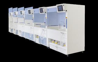
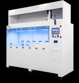
• Wet Benches & Process Stations – Automated lines for etching, washing, and wafer cleaning.
• Chemical Distribution & Dosing – Systems for safe dilution, blending, and slurry distribution.
• Wafer & Chip Handling – High-precision robotic systems and end-effectors for delicate substrates.
• Clean-Room Automation – Single-purpose machines and assembly cells for high-purity environments.
• Optical Inspection Systems – Machine vision for quality control and defect detection.
• Turnkey Custom Engineering – From simulation and design to software, commissioning, and support.
STROZA
Contacts
SVCS Process Innovation Optatova 37 Brno
E-mail info@svcs.com Mobile number +420 517 070 010
Competences & Capabilities
Our experience is based on a long history and tradition of the semiconductor industry in former Czechoslovakia, in a place called the Czech Silicon Valley.
For over 26 years we have been striving towards development of the tomorrow’s tools and tomorrow’s process innovations. To do this successfully, we cooperate with leading R&D laboratories, universities and scientific institutes.
The company’s headquarters and production plant are located in the Czech Republic. We have worldwide network of business representatives.
Equipment
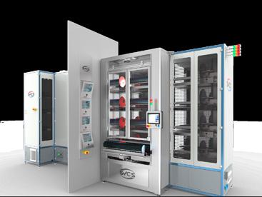
Horizontal/Vertical Furnaces designed for all standard Atmospheric/CVD Processes suitable for Full Production.
All SVCS tools are driven by SV-Con, our in-house designed robust control system, which can also be adjusted for refurbishments of third-party equipment. svcs.com
SVCS has delivered installations for customers all over the Planet, for example: Australia, Belarus, Belgium, Denmark, France, Germany, China, India, Japan, Korea, Lithuania, Malaysia, Mexico, Okinawa, Poland, Slovakia, Sweden, Taiwan, UK and the USA.
Compact Tabletop Furnaces and Single Wafer Reactors designed as a compact solution for R&D sector like institutes or laboratories.
Ultra High Purity Gas Delivery Systems like Gas Cabinets, Valve Manifold Boxes and custom production of gas manifolds.
Swagelok Czech Republic (Central Fluidsystems s.r.o.) is the authorized sales and service center for Swagelok, a global leader in fluid system solutions. As a trusted solution provider for the semiconductor industry, we support tool OEMs, chip fabricators, and gas/chemical suppliers by combining global scale with regional responsiveness—the core of our Global Strength and Local Support. We deliver highly reliable fluid systems designed to meet extreme cleanliness and precise containment standards.
Contacts
Swagelok Czech Republic (Central Fluidsystems s.r.o.)
Na Radosti 420 155 21 Prague
E-mail martin.gorgol@centralfluid.cz Mobile number ++420 797 974 200
Competences & Capabilities
Our extensive product portfolio is tailored for demanding process environments like ALD, etch, and photolithography. Beyond premium components, we supply high-performance ultrahigh-purity (UHP) valves, high-purity weld fittings, metal gasket face seal fittings, UHP inline filters, and insulated hoses for chiller applications. Supported by a strict Cleanliness Chain, these products provide extreme dosing precision and consistent performance over millions of cycles under corrosive media or high temperatures. All products feature robust material standards, full traceability, and double-certified 316/316L stainless steel or special alloys to eliminate leak risks, maximize chip yield, and reduce total lifecycle costs.
To add unparalleled value, we provide customdesigned, pre-tested assemblies, gas distribution systems, and specialized engineering services. Our localized technical support includes Field Engineering, Technical consultation, and
comprehensive On-site services like leak detection audits and fluid system site surveys. For expansions, our Fab Construction Services help reduce man-hours and keep projects on schedule from tool installation to specialty gas distribution. We also conduct technical training, including orbital welding and high-purity fittings essentials.
To keep your operations moving with total confidence, we leverage the full Swagelok Advantage. Driven by a $1.2 billion global inventory and strategic local stocking, we guarantee reliable product availability, helping you maintain fab uptime, maximize throughput, and safely compete in a fast-changing market. www.swagelok.com
Swagelok Czech Republic (Central Fluidsystems)
TechSoft Engineering (TechSoft) is an Ansys Channel Partner providing Ansys software, technical support, training and engineering services. We help companies through the full Ansys simulation portfolio, including structural and thermal analysis, computational fluid dynamics (CFD), electronics, optics and semiconductor applications. TechSoft is a Czech engineering consultancy specialising in simulation-driven product development
Contacts
TechSoft Engineering
Milevská 2095/5
140 00 Prague 4 Czech Republic
www.techsoft-eng.cz
E-mail info@techsoft-eng.cz
Mobile number +420 702 190 645
TechSoft is an engineering and technology partner specialising in simulation-driven product development and digital engineering. As an Ansys Channel Partner, we help organisations shorten development cycles, reduce costs, improve reliability and optimise product performance through engineering simulation and digitalisation. With experience across the automotive, aerospace, energy, semiconductor, electronics, industrial equipment and manufacturing sectors, we support customers throughout the entire product lifecycle— from concept development and virtual prototyping to validation and optimisation.
Competences & Capabilities
Structural mechanics (FEA), vibration and fatigue analysis; thermal management and heat transfer; computational fluid dynamics (CFD); low- and high-frequency electromagnetic simulation; power electronics; signal and power integrity; optical and photonic simulation; digital twins; workflow automation; sustainability assessment; engineering consultancy; simulation
methodology development; and technical training. Our multidisciplinary expertise enables customers to address complex engineering challenges and make informed design decisions based on physics-based simulation.
Products & Services
Ansys software licensing, deployment and maintenance; technical support and customer services; engineering simulation projects; design verification and optimisation; virtual testing; custom simulation workflows; software integration; digital engineering solutions; technical training courses and workshops; and specialist engineering services tailored to customer requirements. Our solutions help companies shorten development cycles, reduce reliance on physical prototypes, minimise technical risk and bring innovative products to market faster.
Tescan, part of Shimadzu Corporation, is a global manufacturer of electron microscopes and advanced scientific instruments. With more than 30 years of innovation, the company develops solutions for materials research, semiconductor manufacturing, life sciences and industrial quality control. Tescan combines deep application expertise with precision engineering to help customers understand, optimise and advance complex technologies.
Contacts
Tescan Libušina třída 21 623 00 Brno
www.tescan.com
E-mail info@tescan.com
Mobile number +420 724 930 599
Competences & Capabilities
Tescan develops and manufactures scanning electron microscopes (SEM), focused ion beam scanning electron microscopes (FIB-SEM), micro-CT systems and integrated analytical solutions that enable characterisation, imaging and microstructural analysis across research and industry. Headquartered in Brno, Czech Republic, the company combines in-house development, manufacturing and application expertise with a global network of sales and service organisations.
Semiconductor technologies represent one of Tescan’s strategic areas of expertise. The company’s solutions support the complete semiconductor value chain, from materials development and process optimisation to failure analysis, quality assurance and advanced packaging. High-resolution imaging, precise sample preparation and three-dimensional characterisation enable customers to investigate increasingly complex device architectures with confidence and efficiency.
Profiles of companies
Tescan works closely with leading semiconductor manufacturers, research institutes and technology centres to develop workflows that address the industry’s evolving challenges. Its instruments integrate advanced automation, artificial intelligence-assisted workflows and multimodal analytical techniques, helping customers increase productivity while delivering reliable and reproducible results.
As part of Shimadzu Corporation, Tescan combines its recognised expertise in electron microscopy with the strength of a global technology group committed to advancing science and industry. Together, the companies provide complementary analytical technologies that accelerate innovation across semiconductor research, advanced materials, electronics and other high-technology sectors.
Tescan
Tescan UniTOM HR 2
Tescan FemtoChisel
Tescan SOLARIS X 2
Tescan TENSOR
Thermo Fisher Scientific In order to reveal what matters, enable what’s critical, and innovate what’s next, we provide purpose-built electrical and physical analysis solutions that help enable lab and fab engineers to develop advanced semiconductor processes while improving yield, productivity, and cost-effectiveness. With over 40 years of semiconductor-focused innovation, we understand the unique challenges you face with increasingly complex technology nodes.
Contacts
Thermo Fisher Scientific
Vlastimila Pecha 1282/12 627 00, Brno
www.thermofisher.com
E-mail jobs.brno@thermofisher.com
Mobile number +420 513 245 111
Competences & Capabilities
Our Mission is to enable our customers to make the world healthier, cleaner and safer. Whether our semiconductor customers’ products find use in the fields of finance, medicine, transportation, or education, we are here to support them with innovative solutions.
With over 40 years of semiconductor-focused innovation, we understand the unique challenges you face with increasingly complex technology nodes. We drive technological evolution for leading global companies while strengthening our expertise and capabilities to fulfil our semiconductor promise to each customer.
Products and Services
Our comprehensive portfolio of electrical fault isolation and characterization techniques, scanning electron microscopes (SEMs), transmission electron microscopes (TEMs), and focused-ion-beam (FIB)SEMs work together as integrated solutions to reveal what is invisible to conventional techniques.
These purpose-built technologies provide detection and analysis with atomic-scale accuracy for ground truth insights essential for complex 3D structures and advanced process development.
What sets us apart is our semiconductor-first approach. Each solution we develop addresses the specific metrology and defect challenges semiconductor customers face daily. Our advanced software suites and automated workflows enable fast time-to-data and operational productivity critical for staying competitive. Our end-to-end comprehensive workflows combine these analytical instruments with dedicated semiconductor expertise to drive technological evolution and innovate what’s next in semiconductor development. Our solutions provide electrical failure analysis, defect characterization, and metrology capabilities for next generation nodes, delivering the faster, clearer path to higher yields and lower costs.
Thermo Fisher Scientific
Tropic Square is a European fabless semiconductor company redefining hardware trust for security-critical embedded systems. Our open-architecture secure elements make the root of trust independently verifiable – replacing security-through-obscurity with transparent design that puts control back in the hands of manufacturers and developers. This transparency invites scrutiny, allowing the system to evolve with the threat landscape.
Contacts
Tropic Square s.r.o. Kundratka 2359/17a 180 00, Prague 8 Czech Republic
www.tropicsquare.com
E-mail welcome@tropicsquare.com
Competences & Capabilities
We design and manufacture zero-trust silicon using RISC-V architecture. Our core competence is building device integrity and genuine trust through radical transparency. Beyond open architecture alone, our transparent vulnerability disclosure equips partners to mitigate risks before they escalate. This proactive security lifecycle makes our hardware ready for the Cyber Resilience Act (CRA) by design, keeping you ahead of new compliance standards. From crypto hardware wallets and industrial IoT to automotive ECUs, edge AI platforms, and autonomous systems, we secure a wide range of critical applications that require both regulatory checklists and the long-term resilience of open architecture.
Products & Services
Our flagship IC, TROPIC01, is the industry’s first fully auditable secure element. It delivers a tamper-resistant Hardware Root of Trust for key management, secure storage, and digital identity. Features include MAC-
Profiles of companies
and-Destroy PIN verification, PUF-derived keys, and robust side-channel attack resilience.
Our open-source ethos also completely transforms the development timeline. Because TROPIC01 operates without restrictive NDAs and our architecture is fully documented, teams can leverage AI assistants directly with our specifications. This empowers developers to experiment faster, verify implementations effortlessly, and integrate seamlessly. TROPIC01 is shipping globally and is available on development boards compatible with Raspberry Pi, Arduino, and Mikroe.
UJP PRAHA a.s. is a Czech high-tech company specializing in semiconductor and radiation-hardened technologies. It provides custom ASIC design, advanced engineering, and radiation hardness testing through its own Laboratory for Radiation Hardness Testing (LTRO) for semiconductor, industrial, medical, space and environmental applications.
Contacts
UJP PRAHA a.s.
Nad Kamínkou 1345 156 10 Prague 5
www.ujp.cz
E-mail gallus@ujp.cz
Mobile number +420 724 385 483
Competences & Capabilities
UJP PRAHA a.s. provides advanced R&D, engineering and manufacturing services for semiconductor, microelectronics and radiation-hardened technologies. The company has extensive experience in custom ASIC design for high-reliability applications and uses a full commercial Cadence IC design environment for frontend and back-end IC development, verification and tape-out preparation. Through collaboration with imec and fabrication access via TSMC, UJP develops and validates custom integrated circuits using advanced semiconductor technologies.
A key capability is the LTRO (Laboratory for Radiation Hardness Testing), established within the IPCEI ME/CT project. The laboratory performs Total Ionizing Dose (TID) testing, long-term irradiation, in-situ electrical characterization during irradiation and qualification of ASICs, semiconductor devices, integrated circuits, sensors and detector systems. Its unique multi-source Co-60 irradiation facility enables flexible irradiation
geometries, parallel testing of multiple samples and a wide range of dose rates.
Products & Services
• Custom ASIC design and verification
• Cadence-based IC design services
• ASIC prototyping and tape-out support
• Radiation hardness testing (TID) in UJP’s LTRO facility
• Qualification of semiconductor devices and electronic assemblies
• In-situ electrical testing during irradiation
• Prototype development, engineering consulting, technology transfer and collaborative R&D
UNITES Systems, a Czech technology company founded in 1991 in Valašské Meziříčí, develops and manufactures advanced measuring and testing equipment for semiconductors, electronic components, and power modules. It provides precise automated testers and fully customised FCT/ICT systems to global customers across electronics, automotive, aerospace, telecommunications, medical, and defence sectors, maintaining ISO 9001 standards.
Contacts
UNITES Systems a.s.
Kpt. Macha 1372
757 01 Valašské Meziříčí
unites-systems.com
Ondřej Běťák Mobile number +420 602 555 872 E-mail obetak@unites.cz
Competences & Capabilities
UNITES Systems a.s. (Est. 1991, Valašské Meziříčí) is a Czech manufacturer of Automated Test Equipment (ATE) for semiconductor components, power modules, and electronic assemblies, with 500+ global clients.
Core Competencies & Capabilities
• ATE Design: In-house R&D of mixed-signal, high-power, and discrete test instruments.
• WBG Testing: Measurement and characterisation of Silicon Carbide (SiC) and Gallium Nitride (GaN) devices.
• Space & Defence: Czech Space Alliance member specialising in radiation-hardened (RAD-HARD) testing and custom adapters.
• Legacy Continuity: Global specialist in retrofitting and life-cycle continuity for legacy platforms like SZ Testsysteme M3000 and UNIMET 3000.
• Software Integration: Proprietary UniLAB and SCADUS (C#-based) ecosystems for parallel multi-site testing and MES integration. ISO 9001 certified.
Primary Semiconductor Testers
Profiles of companies
EFFITEST Platform (Power Semiconductors)
• P100 Series: Tailored for laboratory engineering, device characterisation, and low-volume testing.
• P900 Series: High-speed mass production platform optimised for volume manufacturing and automated handler integration.
• Specs & Features: Up to 5,000V / 1,500A. Production throughput up to 72,000 UPH. Features integrated
Curve Tracer, Virtual Scope, Avalanche (UIS/UIL), and parasitic capacitance (Ciss, Coss, Crss).
UNIMET Platform (Mixed-Signal Laboratory)
Flexible benchtop testers for engineering validation, ASIC characterisation, and incoming QC.
• Coverage: Linear/digital ICs (OpAmps, converters, regulators), discrete components, AD/DA converters, PWMs, voltage regulators, etc.
• Specs: Includes a relay-less microvolt option (less than 1 μV) for precise, repeatable threshold measurement of ICs.
Brno University of Technology (BUT) is a leading Czech technical university developing education, research and innovation for the semiconductor value chain. Through its Czech Semiconductor Centre, European projects and the BUT Semiconductor Hub, it connects chip design, microelectronics, materials, technologies, cleanrooms and industry cooperation.
Contacts
Brno University of Technology
Antonínská 548/1 602 00 Brno
www.vut.cz
E-mail haze@vut.cz Mobile number +420 54114 6102
Competences & Capabilities
BUT builds semiconductor competences across education, research, prototyping, and technology transfer. The Czech Semiconductor Centre (CSC), based at BUT, links academia and industry, supports start-ups and SMEs, offers mentoring and access to European pilot-line and design-platform opportunities, and helps develop the national talent pipeline. BUT also implements initiatives such as Chips of Europe and Semiconductors4All, supporting upskilling, micro-credentials, STEM outreach and closer cooperation between universities and companies.
The BUT Semiconductor Hub brings together activities and teams from many faculties (such as FEEC, FIT, FME, FCH) and CEITEC BUT. Its capabilities cover chip and integrated-circuit design, micro- and nanoelectronics, embedded systems, sensors, testing and characterisation, power and smart-sensing applications, semiconductor materials and processes, mechanical and process engineering, chemistry for advanced materi-
als, cleanroom technologies, and access to advanced analytical and fabrication infrastructure.
BUT offers specialised bachelor’s and master’s education in Chip Design and Modern Semiconductor Technologies, Physical Engineering and Nanotechnology, practical project-based teaching, industry internships and collaboration with companies including onsemi, Codasip and other partners. It provides research collaboration, contract R&D, expert consultation, training and talent development for the Czech and European semiconductor ecosystem.
Cybersecurity Hub An expert organisation on cybersecurity founded by BUT, CTU, and MU. CSH creates an innovation ecosystem forming the future through research, services and infrastructure to strengthen security and resilience. CSH hosts the Advanced Chip Design Research Centre (ACDRC) between Czechia and Taiwan dedicated to cultivating integrated circuit design talent and fostering the development of the semiconductor industry ecosystem in Czechia.
Contacts
Cybersecurity Hub
Šumavská 416/15 602 00 Brno
www.cybersecurityhub.cz
E-mail info@cshub.cz Mobile number +420 778 884 996
Competences & Capabilities
CyberSecurity Hub, z.ú. (CSHub) is a Czech non-profit research and innovation institute headquartered in Brno that connects academia, industry, and the public sector in advanced digital technologies, with a primary focus on cybersecurity, trusted computing, artificial intelligence, and semiconductor innovation. CSHub serves as an independent platform for international collaboration, technology transfer, education, and the coordination of large-scale research initiatives.
One of the major strategic activities of CSHub is the establishment and coordination of the Advanced Chip Design Research Centre (ACDRC), an international initiative launched in cooperation with Taiwan’s National Applied Research Laboratories (NIAR) and supported by the Taipei Economic and Cultural Office (TECO). Within ACDRC, CSHub acts as the Czech coordinating organization, managing collaboration among leading universities, including Brno University of Technology, Czech Technical University in Prague, and Masaryk Uni-
versity, while facilitating partnerships with Taiwanese universities and semiconductor research institutions.
ACDRC focuses on strengthening semiconductor research capabilities in the Czech Republic through collaborative R&D, advanced chip design, EDA methodologies, RISC-V architectures, AI accelerators, electronic design automation, workforce development, student mobility, and joint academic–industrial projects. The initiative aims to build long-term Czech–Taiwan cooperation, develop highly qualified semiconductor engineers, and contribute to the resilience of European semiconductor ecosystems by connecting research excellence with industrial innovation.
The Faculty of Electrical Engineering at the Czech Technical University in Prague (FEE CTU) is one of the leading electrical engineering faculty in the Czech Republic and one of the country‘s most research-intensive academic institutions. Through research, education and international cooperation, FEE CTU contributes to the development of the Czech and European semiconductor ecosystem.
Contacts
Faculty of Electrical Engineering, Czech Technical University in Prague Technická 2, 166 27 Prague 6
fel.cvut.cz/en
Phone number: +420 732 271 307
E-mail jakovenk@fel.cvut.cz (prof. Ing. Jiří Jakovenko, Ph.D.)
Competences & Capabilities
Established in 1950, FEE CTU provides education and research in electronics, microelectronics, electrical engineering, telecommunications, computer engineering, cybernetics and artificial intelligence. The faculty comprises 17 departments and cooperates with leading universities, research organisations and technology companies worldwide.
Semiconductor activities are centred around the Laboratory of Nanoelectronic Technologies at the Department of Microelectronics, equipped for the design, characterisation and testing of nanoelectronic structures. Students at bachelor’s, master’s and doctoral levels gain hands-on experience through research projects with academic staff and PhD candidates.
FEE CTU is an active partner of the Czech Semiconductor Centre (CSC), contributing specialised infrastructure, research expertise and education. The faculty also offers the new Electronics and Integrated Systems
(EIS) degree programme, focused on semiconductor technologies, integrated circuit design and applied electronics, preparing graduates for careers in the semiconductor industry and related sectors.
Together with the Taiwan Semiconductor Research Institute (TSRI), CTU established the CTU–TSRI Joint Research Centre. FEE CTU also organises workshops, summer schools, microcredential programmes and other lifelong learning activities for students and professionals. The faculty has extensive experience in national and international semiconductor projects and participates in competence centres.
CTU is also working on the Taiwanese ACDRC project, which supports the training of new talent in the field of chips, equipment support and scientific projects with TW companies, focusing, for example, on automating the design of analogue integrated circuits using machine learning.
Applied semiconductor research at FZU is carried out mainly through collaborative projects, complemented by services and licensing. Activities focus on laser technologies for semiconductor processing, wide band gap materials (GaN, diamond) and radiation resistant devices. Advanced characterization techniques are also available. FZU integrates fundamental research with technological developments to produce knowledge and innovation.
Contacts
Institute of Physics, Czech Academy of Sciences
Na Slovance 1999/2 182 00 Prague 8
www.fzu.cz/en
E-mail hospodko@fzu.cz Mobile number +420 220 318 401
Competences & Capabilities
FZU builds semiconductor competences across several research field, such as laser technologies for inspection, front-end semiconductor processing and downstream chip production, wide-band gap semiconductors (mainly GaN and diamond) development, development of semiconductor devices which are resistant to ionizing radiation, development of fast scintillators for semiconductor inspection equipment, semiconductors for photovoltaics, thin films, 2D semiconducting materials.
FZU offers a broad set of techniques: epitaxy (MBE, MOVPE), clean room photolithography and electron lithography, plasma etching, and thin film deposition (ALD, CVD, PVD), covering all steps needed for real device development. Advanced nanostructures can be manufactured using FIB technique. FZU also offers numerous advanced semiconductor characterization techniques, accessible through the LNSM facilities within the CzechNanoLab infrastructure (www.czechnanolab.cz).
FZU (HiLASE Centre) develops advanced high energy diode pumped lasers and laser applications for industry, including semiconductor inspection, lithography, wafer processing steps, delivering efficient and reliable laser based manufacturing solutions.
Wide band gap semiconductors development in FZU concentrates on GaN and diamond based devices. Based on GaN d-HEMT as well as e-HEMT structures are developed. Part of the applied research is devoted to development of GaN based fast scintillators.
FZU takes active part in student education, enabling bachelor, master or PhD theses to be done using FZU equipment so that the students get acquainted with available techniques and with the work in clean rooms.
We offer research collaboration, contract R&D, expert consultation, training and talent development for the Czech and European semiconductor ecosystem.
Institute of Physics, Czech Academy of Sciences (FZU)
Heyrovský Institute of the CAS, a public research institution, develops the scientific legacy of the Nobel Prize winner, Professor Jaroslav Heyrovský, in the fields related to physical chemistry. The theoretical knowledge and experimentally acquired knowledge of the physical chemical processes occurring in molecules and atoms are of importance for industrial catalysis, energy production and storage, healthcare and the environment.
Contacts
Heyrovský Institute, Czech Academy of Sciences
Dolejškova 2155/3, 182 00 Prague 8
www.heu.cas.cz
E-mail director@heu.cas.cz Mobile number +420 286 583 014
Competences & Capabilities
Heyrovský Institute of the CAS is a leading Czech public research institution conducting fundamental and applied research in physical chemistry, advanced materials and nanotechnologies with strong relevance to the semiconductor industry. The Institute develops innovative materials, analytical methods and technologies supporting next-generation electronic and optoelectronic devices.
Our expertise covers the synthesis, processing and characterization of 1D and 2D materials, including graphene, transition metal dichalcogenides, carbon nanotubes and related nanostructures. We investigate their electrical, optical and structural properties and integrate them into sensors, transistors and microelectronic devices. The Institute also develops semiconductor oxides, functional thin films, nanostructured materials and electrochemical materials for advanced electronic and energy applications.
Our research infrastructure enables the complete innovation chain, from material synthesis and surface modification to advanced characterization, device fabrication and prototype testing. We employ state-of-the-art spectroscopy, microscopy, lithography, electrical characterization, mass spectrometry and computational modelling. We also develop novel analytical methods, sensor technologies and microfluidic platforms.
The Institute actively collaborates with industrial partners and international research organisations on technology transfer, contract research and joint R&D projects. Our services include materials characterization, development of functional nanomaterials, semiconductor-related sensor technologies, prototype development, analytical measurements and scientific consulting.
The Institute of Photonics and Electronics (ÚFE) is a public research institution and part of the Czech Academy of Sciences, the largest Czech non-university research organisation. ÚFE contributes to the development of knowledge and cutting-edge technologies in electronics, optoelectronics, and photonics, linking excellent fundamental research to industry-oriented innovations
Contacts
Institute of Photonics and Electronics
Chaberská 1014/57
182 00 Prague 8
www.ufe.cz
E-mail ufe@ufe.cz
Phone +420 266 773 404
Competences & Capabilities
ÚFE’s competencies in the semiconductor field are centred on the synthesis, modeling, and advanced characterization of wide-bandgap semiconductor thin films and nanostructures for electronic, optoelectronic, and sensing applications. ÚFE focuses on the preparation of epitaxial and nanostructured metal-oxide semiconductors using solution growth methods and mist chemical vapour deposition. Its activities extend beyond the conventional experimental approach by modelling chemical and physical phenomena during growth, identifying nucleation and growth mechanisms, and developing new growth methods, reactors, and patterning strategies.
ÚFE has strong expertise in the use of laser, electron-beam, and ion-beam lithography in semiconductor technologies. Focused ion beams are employed for local patterning and controlled nucleation, enabling the growth of ordered arrays of nanostructures and prototype nanoscale devices with desired properties.
ÚFE studies ion-beam interactions with semiconductor substrates and uses focused ion beams to tailor the properties of semiconductor surfaces and interfaces.
ÚFE provides advanced optical and electrical characterisations of semiconductor materials and individual nanostructures, including photoluminescence measurements over a broad spectral and temperature range, as well as in-situ electrical probing of single nanostructures and their heterojunctions directly in a scanning electron microscope.
The foundation of fundamental semiconductor materials research has also been translated into application-oriented work targeting the design and characterisation of functional prototypes of semiconductor devices, including ultraviolet photodetectors and light sources, transparent electronic devices, and gas sensors based on nanostructured semiconductors.
Institute of Photonics and Electronics, Czech Academy of Sciences (ÚFE)
Institute of Physics of Materials, Czech Academy of Sciences A research institute focused on developing and optimising the performance of advanced materials, shaping innovations in energy, transport, aerospace, automotive, and medical fields. By combining experimental characterisation with computer simulations and quantum-mechanical calculations, we harness the potentials of new materials and nanostructures relevant for semiconductor and electronic applications.
Contacts
Institute of Physics of Materials, Czech Academy of Sciences
Žižkova 513/22 616 00 Brno
E-mail groger@ipm.cz (Assoc. Prof. Roman Gröger)
Mobile number +420 732 327 328
Competences & Capabilities
The institute covers the full chain of materials research, from synthesis to in-depth characterisation and modelling. Material structure is studied using transmission and scanning electron microscopy, EBSD, FIB and scanning probe microscopy, down to the atomic level, complemented by EBIC for semiconductor characterisation. Mechanical testing includes creep, low- and high-cycle fatigue (up to gigacycle regimes), and strength testing across a wide temperature range, from -196 °C to 1500 °C. Thermodynamic and thermophysical properties, including hydrogen sorption, are measured by calorimetry and gas-sorption methods.
Magnetic, electrical and transport properties are assessed from cryogenic to elevated temperatures. New materials are developed using powder metallurgy, casting, milling and 3D printing for metals, ceramics and polymers. Numerical simulations span ab initio calculations, CALPHAD modelling, crystal plasticity and finite element methods, including atomistic studies
of defect formation in III-nitride films and MBE-based investigation of early-stage AlN/Si growth.
Products & Services
The institute offers analysis and consultancy services for industrial and academic partners, including semiconductor and nanostructure characterisation, microstructural analysis, failure investigation and material development. It also designs and supplies its own equipment, such as gravitational-loading creep machines and ultrasonic giga-cycle fatigue testing devices, tailored to customer requirements, including sales, distribution and service support.
A novel device for characterising superparamagnetic nanoparticles for magnetic hyperthermia is currently under development. www.ipm.cz
The E-Beam Lithography Group of ISI CAS offers a full range of services for the prototyping of semiconductor structures and chips on substrates of up to 6 inches in diameter. The group‘s capabilities include electron beam lithography, resist deposition, plasma and wet etching, magnetron sputtering, and lift-off processes. The group also develops photomasks for optical applications and magnetic nanostructures, as well as structured SiN membranes that enable advanced electron-beam shaping and manipulation.
Contacts
Institute of Scientific Instruments, Czech Academy of Sciences
Královopolská 147 612 00 Brno
www.isibrno.cz
E-mail csc@isibrno.cz
Competences & Capabilities
The EBL Group at ISI Brno offers a wide range of services in electron beam lithography and the micro-/nanofabrication of semiconductors and other functional materials. The fabrication process typically begins with the selection and preparation of suitable substrates, such as silicon, sapphire and glass, in formats of up to 6inch wafers or masks, depending on the application. Appropriate surface treatment and cleaning procedures are then applied to ensure high process quality and reproducibility.
The lithographic workflow generally involves applying high-resolution electron-beam resists and converting customer designs into formats compatible with electron beam patterning systems. The structures are then defined by focused electron beam exposure, which enables the fabrication of complex micro- and nanoscale features with high precision and dimensional control.
After defining the pattern, the exposed structures are developed and processed according to the specific application requirements. The resulting resist pattern can be used as either a mask for material removal processes (including wet etching, plasma etching and reactive ion etching (RIE)) or a template for the selective deposition of functional materials (such as metals) using magnetron sputtering.
The fabrication process is completed by removing the resist and carrying out any additional post-processing steps required to achieve the desired structure and functionality. By integrating these technologies, EBL Group supports the entire fabrication process, from design preparation and process development to creating advanced micro- and nanostructures, prototypes and functional devices for research and industrial applications.
University of Jan Evangelista Purkyně in Ústí nad Labem (UJEP) advances research in semiconductor chemistry, focusing on high-purity chemicals and precursors for semiconductor fabrication, including their synthesis, characterisation, and optimisation for use in electronics, photonics, and energy technologies, with strong emphasis on innovation, interdisciplinary collaboration, and practical applications in industry.
Contacts
Department of Chemistry, Faculty of Science UJEP
Pasteurova 3632/15
400 96 Ústí nad Labem
chemistry.ujep.cz/polovodicova-chemie/
E-mail Martin.babor@ujep.cz
Mobile number +420 604 240 754
Competences & Capabilities
UJEP provides expertise in semiconductor-related chemistry with a strong focus on high-purity chemicals and precursor systems, including process gases, ultrapure water, and key industrial chemicals such as mineral acids. Core competences include the development of innovative synthetic routes for input materials, impurity control, pre-purification strategies prior to final refinement, and optimisation of existing chemical processes and material flows.
The team specialises in inorganic and organometallic synthesis, trace impurity analysis at very low concentration levels, and advanced physicochemical characterisation (structural, thermal and spectroscopic methods). Particular emphasis is placed on identifying contamination sources, chemical stability, reproducibility and scaling of laboratory procedures relevant to industrial practice.
Activities focus on upstream chemical development and conditioning of input materials rather than device fabrication, without reliance on cleanroom facilities. Services include custom synthesis of specialised chemicals and precursor systems, analytical and physicochemical characterisation, impurity profiling and control strategies, optimisation of existing processes and flows, and collaborative research on new preparation routes and treatment methods for semiconductor-grade chemicals within industrial supply chains.
JIC is a Czech innovation agency and member of the Czech Semiconductor Centre consortium. With over twenty years of experience supporting more than 1,300 startups and ranked among Europe‘s fifty best startup hubs by the Financial Times in 2026, JIC supports ambitious projects from first idea through growth, investment and international expansion, while strengthening technology transfer and the wider innovation ecosystem.
Contacts
JIC Innovation Agency
Purkyňova 127 612 00 Brno-Medlánky
www.jic.cz
E-mail vrbkova@jic.cz
Mobile number +420 602 575 646
Competences & Capabilities
As a member of the CSC consortium – a six-partner initiative bringing together industry and academia to strengthen the Czech semiconductor value chain – JIC contributes its expertise in research commercialization, startup development and funding strategy.
It works across the full innovation lifecycle – from early-stage academic research to market-ready companies – backed by an extensive network of mentors, investors and ecosystem partners across Czech Republic and beyond. As a long-standing member of the Enterprise Europe Network, JIC also facilitates international partner matching and cross-border R&D collaboration for semiconductor clients.
For academics and scientists – including PhD students and researchers in semiconductor-related fields – JIC offers structured training in identifying and realizing the commercial potential of research projects. Topics span spin-off creation, technology transfer, IP strategy and
business validation, with the goal of generating new startups from Czech university research in semiconductor technologies.
Entrepreneurs at the earliest stages receive one-toone consultancy over several months, guiding them through company formation, business model development and investment readiness, with longer-term support as the business grows and prepares to enter domestic and international markets.
JIC also provides individualized advisory on funding strategy, helping semiconductor startups and SMEs identify the most suitable combination of grants –including the EU Chips Fund, EIC Accelerator and Horizon Europe – and private investment, with handson support for application preparation and investor introductions. Early-stage projects may also be considered for investment by JIC Ventures – JIC’s own VC fund focused on (pre)seed deep tech projects from the CEE region.
The Faculty of Science at Masaryk University has a long history of education and research in several STEM fields, including the physics of semiconductors. It runs well-equipped laboratories, including a unique educational cleanroom facility for silicon device technology. The Faculty of Informatics focuses its hardwarerelated activities on the design, validation, and verification of modern digital systems and silicon chips.
Contacts
Masaryk University (Faculty of Science & Faculty of Informatics)
Kotlářská 2 602 00 Brno
www.muni.cz
E-mail munzar@physics.muni.cz, matej@muni.cz Mobile number +420 604 240 754
Competences & Capabilities
Two faculties of the Masaryk University have major competences in the field of semiconductors and chips. We provide an excellent standard of education and carry out research activities devoted to physics, technology, software and hardware. We run high-tech laboratories, develop software, and conduct R&D projects with industrial partners.
Faculty of Science
The research at the Department of Condensed Matter Physics is focused on optical and structural characterisation of semiconductor materials, thin films and nanostructures, and prospective new materials. The optical methods include ellipsometry, spectroscopy and reflectometry for a large spectral range from far-IR to near-UV, and Raman scattering. The structural analysis covers a variety of X-ray diffraction and other scattering techniques. The Department of Plasma Physics and Technology conducts research on thin-film deposition
by sputtering of various materials for semiconductor technology. We run cleanroom laboratory to provide education for university students from the whole country, demonstrations for secondary school students and hands-on courses for staff of companies.
Faculty of Informatics
The EmLab laboratory focuses on the design, validation and verification of modern digital systems and silicon chips. We develop specialised chips and hardware architectures for computational acceleration, including applications in numerical simulations, signal processing and artificial intelligence. We design hardware and electronic systems for high-speed data processing from ionising radiation detectors, mainly for experiments conducted at nuclear reactors, particle accelerators and other radiation sources. EmLab provides an environment for developing and verifying advanced hardware solutions from initial design to real-world deployment.
Palacký University Olomouc supports the Czech semiconductor ecosystem through the Faculty of Science and CATRIN. It combines expertise in optics, photonics, nanomaterials, functional materials, thin films, advanced characterisation and modelling with state-of-the-art infrastructure, education and technology transfer for research and industry collaboration.
Contacts
Palacký University Olomouc
Křížkovského 8 771 47 Olomouc
www.upol.cz
E-mail info@upol.cz Mobile number +420 585 631 111
Competences & Capabilities
Palacký University Olomouc connects the Faculty of Science and CATRIN (Czech Advanced Technology and Research Institute). The Faculty of Science provides research and education in physics, optics, chemistry, mathematics, computer science and related natural sciences, supported by modern laboratories and stateof-the-art equipment. CATRIN adds interdisciplinary excellence in advanced materials, nanotechnology, energy, biotechnology and technology transfer. Together they offer expertise relevant to semiconductor R&D, including functional and semiconductor materials, low-dimensional and nanostructured materials, graphene derivatives, thin films and surfaces, optoelectronic and photonic systems, quantum optics, sensors, catalysis and energy materials. Available capabilities include synthesis and modification of materials, surface engineering, advanced microscopy, spectroscopy, structural and chemical analysis, computational modelling, data analysis and prototype-oriented research with academic and industrial partners.
Products & Services
• Contract and collaborative research
• expert consulting
• materials synthesis and optimisation
• nanomaterials and 2D-materials engineering
• thin-film and surface modification studies
• advanced materials characterisation
• optical, photonic and spectroscopic measurements
• electron microscopy and surface analysis
• computational modelling and materials design
• support for grant-based and industry-led R&D
• licensing and technology transfer
• access to selected research infrastructure
• education, training and talent development for the semiconductor sector
Palacký University
Olomouc
Tomas Bata University in Zlín (TBU) is a research-oriented public university with strong links to industry, innovation, and international collaboration. It develops a multidisciplinary approach to semiconductor technologies by integrating education, research and technology transfer across several faculties and Research centres in close cooperation with industrial partners.
Contacts
Tomas Bata University in Zlín nám. T. G. Masaryka 5555 760 01 Zlín
www.utb.cz
E-mail rektor@utb.cz Mobile number +420 576 032 222
Competences & Capabilities
TBU integrates expertise from the Faculty of Technology, Faculty of Applied Informatics and Faculty of Management and Economics to address key segments of the semiconductor value chain. Core competences include semiconductor and electronic materials, materials engineering, chemistry, manufacturing processes, automation, digital technologies and data driven solutions, as well as innovation management and technology commercialisation.
This interdisciplinary approach is supported by modern research infrastructure and strong industrial partnerships, enabling efficient transfer of knowledge into practice. The university also benefits from the Centre of Polymer Systems, contributing expertise in polymer and hybrid materials for microelectronics, including encapsulation systems, functional layers and advanced composites, together with facilities for material design, characterisation and testing.
Products & Services
TBU provides specialised education, applied research, technology transfer and collaborative R&D for semiconductor-related industries and public institutions. The Faculty of Technology leads the Semiconductor Materials specialisation, developed with industrial partners and supported by laboratory training, project-based learning and internships.
Services include contract research, materials development and testing, advanced characterisation, expert consultancy, support in hardware and digital solutions, student projects and professional training. The university also enables pilot-scale experimentation, prototyping and long-term collaboration tailored to partners developing innovative material solutions and technologies for semiconductor applications, with support from the Centre of Polymer Systems.
Tomas Bata University in Zlín
The University of Chemistry and Technology (UCT) Prague is a leading Czech university in chemistry, materials science and chemical engineering. It combines strong fundamental research with applied technology development and industry collaboration. In semiconductors, it contributes expertise in advanced functional materials, 2D materials, nanofabrication-oriented chemistry, characterisation and training for the emerging chip ecosystem.
Contacts
University of Chemistry and Technology, Prague Technická 5, 166 28 Prague 6Dejvice
E-mail info@vscht.cz
Competences & Capabilities
UCT Prague has strong expertise in advanced functional materials relevant to semiconductor technologies, especially layered and two-dimensional (2D) materials. Research teams routinely prepare and study 2D crystals and related compounds, including semiconductors, insulators, conductive, magnetic and other functional layered materials. The university has experience in chemical vapour transport, flux and related crystal-growth approaches, as well as exfoliation and the preparation of materials for both fundamental studies and device-oriented collaborations. fundamental studies and device-oriented collaborations.
Current competences include synthesis of bulk layered crystals, preparation and handling of exfoliated 2D materials, surface and interface chemistry, chemical functionalisation, ink and dispersion concepts, and integration of 2D materials into collaborative research on electronic, optoelectronic, catalytic and sensing technologies. UCT Prague also has practical expertise in the
transfer and encapsulation of 2D materials, including hBN-based protection of flakes on substrates.
The university offers broad analytical and characterisation capabilities for semiconductor-relevant materials: Raman and FTIR spectroscopy, X-ray diffraction (XRD), X-ray photoelectron spectroscopy (XPS), scanning electron microscopy with energy-dispersive spectroscopy (SEM-EDS), atomic force microscopy (AFM) and access to advanced electron microscopy in cooperation with specialised facilities. These techniques support detailed investigation of crystal structure, composition, surface chemistry, defects, interfaces, and material quality.
UCT Prague actively participates in European and international research collaborations on graphene-related and other 2D materials, printed and flexible electronics, and advanced materials discovery, supporting innovation across the semiconductor ecosystem.
University of Chemistry and Technology, Prague
The Faculty of Chemical Technology is the oldest faculty at the University of Pardubice, with a strong focus on science and innovations. Its key areas include materials engineering, nanotechnologies, environmental and chemical engineering, and applied chemistry, integrating education with cutting-edge research and international collaboration.
Contacts
University of Pardubice Studentská 573 532 10 Pardubice
E-mail dekanat.fcht@upce.cz Mobile number +420 466 037 294
Competences & Capabilities
The Faculty of Chemical Technology provides advanced expertise in materials research and semiconductor-related technologies, with a strong emphasis on nanomaterials (0D–2D), thin films and functional surfaces. Its competences cover the design, synthesis, modification and characterisation of advanced materials, including quantum dots, nanotubes, nanofibres and nanosheets.
A key part of the faculty’s infrastructure is the Centre of Materials and Nanotechnologies (CEMNAT), a research infrastructure for both basic and applied research with particular significance in the field of one- and two-dimensional nanomaterials. CEMNAT sets new trends in their synthesis and practical application and supports cutting-edge developments in advanced material systems.
The faculty is equipped with state-of-the-art instrumentation enabling a wide range of scientific and technological capabilities. These include atomic layer
deposition for highly controlled thin functional layers, fibre synthesis technologies for polymeric and inorganic materials, and dual-beam electron microscopy for high-resolution imaging, surface modification and micro- and nanostructuring.
These facilities support both fundamental and applied activities, with applications in energy conversion and storage, optoelectronics, micro- and nanoelectronics, and surface engineering. Open-access infrastructure and strong collaboration with academic and industrial partners enable a broad portfolio of services, including material design and development, advanced testing and characterisation, surface engineering solutions, and expert consultancy tailored to industrial needs.
fcht.upce.cz
The University of West Bohemia in Pilsen (UWB) conducts research across the semiconductor value chain, from power electronics devices to quantum materials. Its competences span two research sectors: Engineering & Technology (Prof. Zdeněk Peroutka) – power semiconductors and power electronics via the RICE centre – and Natural Sciences (Prof. Jan Minár) – quantum materials and technologies at the NTC centre.
Contacts
University of West Bohemia in Pilsen
Univerzitní 8, 301 00 Pilsen
E-mail ceorice@fel.zcu.cz
Mobile number +420 377 634 100
Competences & Capabilities
UWB structures its semiconductor activities into two strategic research sectors, each led by a Research Sector Leader.
Engineering & Technology – Prof. Zdeněk Peroutka
Power semiconductors and power electronics, delivered through the Research and Innovation Centre for Electrical Engineering (RICE): characterisation, qualification and optimal use of wide-bandgap devices and materials (SiC, GaN, diamond, AlN, Si3N4); customised power modules and converters – multilevel, hybrid ANPC (Si IGBT + SiC), MMC, solid-state transformers – with ultra-high power density and embedded intelligence; AI-assisted bare-die layout, embedded SoC, firmware and diagnostics; ceramic substrates and additive Ag/Cu metallisation. RICE covers the complete power-device back-end under one roof – design, parametrisation, packaging, bonding, assembly and testing.
• Joint projects, doctoral training and technology transfer www.zcu.cz
Natural Sciences – Prof. Jan Minář
Quantum materials and technologies linked to semiconductors, at the New Technologies Research Centre (NTC): computational materials design and advanced spectroscopy (ARPES), targeting integrated circuits, sensors and energy-efficient electronic devices.
Products & Services
• Contract R&D from concept to functional prototype and full testing
• Custom power modules and converters for traction (750 V / 1.5 / 3 kV DC), energy (STATCOM, HVDC, storage) and low-voltage GaN/SiC applications
• Power-electronics laboratories testing up to 4 MW; accredited testing laboratory No. 1090 (ČSN EN ISO 17025)
University of West Bohemia in Pilsen
The Faculty of Materials Science and Technology (FMST) is a modern educational institution that combines excellent teaching, cutting-edge research, and close collaboration with industry. We specialize in materials science, advanced manufacturing technologies, nanotechnology, innovations and design of medical devices, and computational technologies in materials science. Our students gain practical experience and the skills needed to shape the sustainable technologies and industries of the future.
Contacts
VSB – Technical University of Ostrava 17. listopadu 2172/15 708 00 Ostrava-Poruba
www.fmt.vsb.cz/en
E-mail katerina.skotnicova@vsb.cz Phone number +420 596 993 404
Competences & Capabilities
FMST at VSB–TUO has a long tradition in materials research. As modern technologies increasingly rely on advanced materials, thin films, nanostructures, and precise control of material properties, it is natural for the faculty to dedicate part of its expertise to supporting the Czech semiconductor ecosystem. Semiconductor-related activities at FMST build on extensive expertise in optical spectroscopy, ellipsometry and advanced materials characterization. While broader cooperation in this field is coordinated by the VSBTechnical University of Ostrava Semiconductor Section, led by Assoc. Prof. Kateřina Skotnicová, the main scientific activities are concentrated at the Department of Materials Engineering and Recycling, where they are developed by the research team of Assoc. Prof. Kamil Postava.
The research team focuses on the research and development of materials and technologies important for next-generation semiconductor devices. This research
includes not only SiC but also emerging wide-bandgap materials such as GaN and diamond. A key strength of the team is its deep expertise in optical methods, namely ellipsometry, spectrophotometry and polarimetry, used for the characterization of the complete permittivity tensors of advanced materials. This expertise provides a strong basis for optical modelling and for the development of fast, contactless and non-destructive characterization methods covering a broad spectral range from the near-UV to the THz region. These methods make it possible to probe semiconductor layers and investigate their electrical, optical and structural properties without causing damage. Alongside advanced characterization, the faculty also develops technologies for preparing thin films and micro- and nanostructures using deposition methods, UV lithography and laser lithography.
The Innovation Centre of the Usti Region (ICUK) builds the regional innovation ecosystem in Northern Bohemia. As a member of the Czech National Semiconductor Cluster, it connects companies, research organisations and investors with Czech and international semiconductor opportunities, with strong links to the Saxon and Taiwanese ecosystems and regional strengths in industrial chemistry, recycling, energy and smart manufacturing.
Contacts
Innovation Centre of the Usti Region (ICUK)
Velká Hradební 2800/54
400 01 Ústí nad Labem
www.icuk.cz
E-mail sivicek@icuk.cz
Mobile number +420 774 320 083
Competences & Capabilities
ICUK is a regional innovation agency founded by the Regional Authority, J. E. Purkyně University and the Regional Chamber of Commerce. It helps companies develop innovation-driven activities and strengthen their role in semiconductor-related value chains.
ICUK turns regional assets into projects and partnerships: a location between Prague and Saxony/Dresden; an industrial base in chemistry, energy, materials, machinery and recycling; and growing R&D and education capacities. Through CNSC, the Czech Semiconductor Centre, CzechInvest and partners, ICUK serves as a regional contact point for investors, suppliers, startups and research teams. As part of CNSC, it provides access to platforms such as Silicon Europe and SEMI, and to wider European chip competence networks.
ICUK provides business and innovation consultancy, feasibility assessment and concept validation, startup incubation (Startup Go), SME acceleration (ICUK
Platinn), innovation vouchers, digitalisation support through its DIH/DigiLab, and mentoring. It helps companies validate business models, identify funding, prepare innovation projects, find partners and enter international markets.
For the semiconductor ecosystem, ICUK focuses on supplier development, upgrading pathways and soft-landing support rather than chip design or manufacturing. It maps regional capabilities, scouts potential suppliers, brokers access to prototyping, testing and infrastructure via Czech and cross-border partners, supports localisation and aftercare for foreign companies, and promotes opportunities in semiconductor chemicals, gas logistics, advanced manufacturing, circular economy and resource efficiency. ICUK contributes to RIS3 and transformation strategy implementation in the Usti Region and participates in EBN/EU|BIC and Regional Innovation Valleys.
Innovation Centre of the Usti Region (ICUK)
Regional Authority of Pilsen region Industrial innovation and development is ingrained in Pilsen Region. It provides for global industrial output, but it also defines the added values on the job market, production capacities and trajectories for the future. Higher education institutions have been an integral part of the Pilsen Region’s educational system for over 70 years, with a natural center in Pilsen, where the University of West Bohemia as well as the Faculty of Medicine of CU are located.
Contacts
Regional Authority of Pilsen region
Riegrova 1
301 00 Plzeň
www.getsmart.cz/en
E-mail uhlik@rra-pk.cz
Mobile number +420 377 201 411
Competences & Capabilities
Semiconductor technologies are identified as one of three promising technological areas that can significantly contribute to the long-term competitiveness of the Pilsen Region (AI, quantum technologies, semiconductors), see www.inovujtevpk.cz/en.
Semiconductor technologies in the Pilsen Region are the focus of both research (primarily in connection with the University of West Bohemia in Pilsen) as well as applied industries, particularly in the field of so-called power electronics (e.g., in connection with the development and manufacture of vehicles, equipment for energy production and distribution, etc.), but also the development of tools used in semiconductor manufacturing (e.g., vacuum chambers or laser micromachining, etc.). For semiconductor development, its testing within various application there is the potential for interdisciplinary collaboration. Mainly within the Pilsen Region’s areas of specialization, which includes:
research on metallic materials, modern mobility, intelligent manufacturing systems, energy, and biomedicine. Quantum technologies, which are the focus of research centres at the University of West Bohemia, offer unique capabilities for the future of semiconductors. This potential also includes world-class educational resources provided by the technical faculties of the University of West Bohemia (www.zcu.cz/en).
One of the most significant developments in this sector was Pilsen region joining ESRA, the alliance of European regions. One of the main missions of this alliance is to collaborate on the preparation and implementation of certain instruments supporting the development of semiconductor technologies, notably the CHIPS Joint Undertaking (CHIPS JU) as an instrument of the Chips for Europe initiative under the European Chips Act.
The South Moravian Region is the Czech Republic‘s first region to join the European Semiconductor Regions Alliance (ESRA), a grouping of Europe‘s most advanced territories in the chip and semiconductor sector. As the country‘s hub for semiconductor activity, the region actively co-creates the national ecosystem through strategic policy, targeted funding, and cross-border collaboration.
Contacts
South Moravian Region
Žerotínovo náměstí 449/3 601 82 Brno
jmk.cz
E-mail posta@kr-jihomoravsky.cz Mobile number +420 541 651 111
Competences & Capabilities
The South Moravian Region brings long-term strategic and institutional competence in building semiconductor ecosystems at regional level. It was the first Czech region to join ESRA, positioning itself within Europe’s most advanced semiconductor territories and gaining direct access to shared knowledge, policy coordination, and international partnerships across the continent. Through its ESRA membership, the Region participates actively in European policy processes shaping the future of chip manufacturing and research.
The Region provided the foundational funding that enabled the preparation of the Czech Semiconductor Centre (CSC) – backing the project through its Smart Accelerator programme at a stage when no national or EU-level financing was yet available. This early commitment proved critical: the CSC proposal was subsequently ranked fifth-best in the pan-European DIGITAL CHIPS Joint Undertaking competition.
The Region supports the semiconductor sector through targeted grant instruments and its role as a convener of public, academic, and industrial stakeholders. Together with the City of Brno and four Brno universities it co-established the innovation agency JIC – a member of the CSC serves as a bridge between the regional innovation ecosystem and semiconductor startups and SMEs.
The Region’s semiconductor strengths span two distinct domains: chip design, with around 500 experts in Brno working on chip architecture and EDA software development, and electron microscopy – one in three electron microscopes produced globally comes from Brno – a technology critical across the entire semiconductor value chain.
South Moravian Region
The Usti Region is a public authority driving Northern Bohemia’s transformation into a competitive industrial region. With the Triangle strategic industrial zone, brownfield and post-mining redevelopment potential, technical schools and a location within about one hour of Prague and Dresden, it supports semiconductor-related investors, suppliers, chemistry-based value chains and first Taiwanese investments.
Contacts
Ústí nad Labem Region
Velká Hradební 3118/48 400 01 Ústí nad Labem
www.kr-ustecky.cz
E-mail tomesovai@kr-ustecky.cz Mobile number +420 733 613 018
Competences & Capabilities
The Usti Region is the public authority responsible for regional development, education and transformation in Northern Bohemia. Its role in the semiconductor ecosystem is to create enabling conditions: investment readiness, skills, infrastructure planning and policy coordination, while company-level innovation services are delivered through ICUK and partners.
As one of ICUK’s founders, the Region uses this platform, together with UJEP, the Regional Chamber of Commerce, CzechInvest and municipalities, to connect education, research and business needs. It supports RIS3 implementation in fields relevant to semiconductor supply chains: chemistry, energy, machinery, materials, digitalisation and circular economy.
A key asset is the Triangle strategic industrial zone, owned by the Region and located near Žatec, with access to the D7 corridor. The Region also seeks to transform brownfields and post-mining areas into places for
higher-value production, services, R&D and skills.
Its position between Prague and Dresden, with road, rail and Elbe links, supports multimodal logistics and access to Czech, Saxon and European markets. This is relevant for semiconductor chemicals, gases, component cleaning, manufacturing and supplier services. The area is already becoming a target for Taiwanese semiconductor-linked investment, including TaMiCo’s planned facility in the Triangle zone and i-TRANS Global’s planned European logistics centre for semiconductor chemicals.
As the authority responsible for secondary schools, the Region supports technical and vocational education, polytechnic skills and school-company cooperation. For investors and partners, it offers political anchoring, links to education and infrastructure planning, and support in aligning projects with regional transformation and competitiveness priorities.
The Zlín Region, one of the 14 self-governing regions in the Czechia, is the region with long industrial tradition. With companies onsemi and NXP, located in Rožnov pod Radhoštěm, the Zlín Region is the leader of the Czechia semiconductors production and innovation. Since 2024, the Zlín Region is an active member of the Czech National Semiconductor Cluster (CNSC) as well as the European Semiconductor Regions Alliance (ESRA).
Contacts
Zlín Region
třída Tomáše Bati 21 761 90 Zlín
www.zlinskykraj.cz
E-mail podatelna@zlinskykraj.cz
Competences & Capabilities
The Zlín Region sits in the South East corner of the Czechia, with good access to international airports in Vienna, Prague and Brno. The population of the region is around 580.000 inhabitants and its economic performance (GDP per capita), reaches around 75 % of the EU average.
The Zlín Region is thanks to its creativity known as a region with a live creative spirit. The creative industries together with semiconductors & microelectronics, plastics & composites, aerospace & defence, precise machinery and IT are key smart specialisation domains of the region.
The regional city of Zlín is the administrative and economic centre of the region. The crucial contribution to the development of this city was made by Tomáš Baťa in the first half of the 20th century. His shoe making company “Bata”, established in Zlín, reached worldwide success. Today the Zlín is shaped by Baťa’s entrepre-
neurial legacy, blending functionalist architecture with modern development. And it is home to Tomáš Baťa University, a leader in polymer sciences, nanotechnology, and industrial design. Currently, the Tomas Bata University is investing heavily in enhancing its education and research capabilities in the field of semiconductors.
A strong focus on innovation together with high-quality education system offers a unique opportunity for people and investors looking for a dynamic and prosperous region with a good quality of life, rich industrial tradition and skilled workforce. Furthermore, the Regional Innovation Strategy and an established ecosystem ZLINNOVATION which links key public, private and academic players in the field of innovation helps to turn the innovative ideas into successful business in the Zlín Region. The main public supporting organizations are TIC (Technology Innovation Centre) and ZRIA (Zlín Region Investment Agency).
The project no. 101217762 is supported by the Chips Joint Undertaking and its members, with additional funding from the Ministry of Education, Youth and Sports of the Czech Republic. Co-funded by the European Union. Views and opinions expressed are however those of the author(s) only and do not necessarily reflect those of the European Union or the Chips Joint Undertaking. Neither the European Union nor the granting authority can be held responsible for them.