
International Research Journal of Engineering and Technology (IRJET) e-ISSN: 2395-0056
Volume: 13 Issue: 03 | Mar 2026 www.irjet.net p-ISSN: 2395-0072

International Research Journal of Engineering and Technology (IRJET) e-ISSN: 2395-0056
Volume: 13 Issue: 03 | Mar 2026 www.irjet.net p-ISSN: 2395-0072
Vegireddi Gitanjali1, Gurivelli Sandeep2, Kondagorri Bhumika3, Moyyi Surya Kumari4, Muvvala Spandana5, Kella Mohan6, Gudepuvalasa Ramesh7
1Avanthi'S St.Theressa Institute of Engineering & Technology Vizianagaram, India
2Dept. of Electronics & Communication Engineering Avanthi'S St.Theressa Institute of Engineering & Technology Vizianagaram, India
3 Dept. of Electronics & Communication Engineering Avanthi'S St.Theressa Institute of Engineering & Technology Vizianagaram, India
4 Dept. of Electronics & Communication Engineering Avanthi'S St.Theressa Institute of Engineering & Technology Vizianagaram, India
5 Dept. of Electronics & Communication Engineering Avanthi'S St.Theressa Institute of Engineering & Technology Vizianagaram, India
6 Dept. of Electronics & Communication Engineering Avanthi'S St.Theressa Institute of Engineering & Technology Vizianagaram, India
Abstract Low-depth quantum arithmetic is essential for reducing latency, decoherence, and power consumption in quantum and quantum-inspired computing systems. While CNOT and Toffoli gates are commonly used, alternative reversible gates can further optimize circuit depth, area, and energy efficiency when mapped to VLSI hardware. This work presents a VLSI-oriented realization of low-depth quantum arithmetic using Peres, Fredkin, and HNG gates. These gates enable compact arithmetic implementations by combining multiple logical functions within single reversible units, thereby reducing gate count and critical path length. The proposed approach maps low-depth quantum arithmetic operations such as addition and comparison onto CMOS-based reversible logic, ensuring minimal information loss and reduced switching activity. HDL-based simulation and synthesis results demonstrate improvements in depth, area, and power consumption compared to conventional CNOT/Toffoli-dominated designs. This work provides an efficient hardware mapping framework for quantum arithmetic suitable for quantum simulators, control electronics, and energy-efficient quantum-inspired accelerators. Further, hybrid reversible gate libraries combining Peres, Fredkin, and HNG gates with adiabatic CMOS techniques are devised to further minimize power dissipation. Optimizing gate selection based on arithmetic depth and switching activity can significantly reduce energy consumption while preserving computational accuracy, making the architecture suitable for low-power quantum control and edge-level quantum-inspired processors.
Keywords— Low-Depth Quantum Arithmetic, Reversible Logic, Peres Gate, Fredkin Gate, HNG Gate, VLSI Implementation, Quantum-Inspired Computing, Low-Power CMOS, Reversible Arithmetic Circuits, Energy-Efficient Hardware.
Introduction
Transistorscaling,performanceoptimization,andarchitecturalparallelismhavehistoricallypropelledthedevelopment of computingarchitectures.However,fundamentalphysicalandthermodynamicconstraintslimittraditionalscalingpatterns asCMOStechnologymovesclosertodeepsub-micronandnanoscaleregimes.Leakagecurrents,heatdensity,interconnect parasitics,anddynamicswitchingpowerallworktogethertorestrictadditionalperformanceimprovements.Information loss is a fundamental aspect of computation in irreversible logic circuits. A direct correlation between information destruction and heat generation is established by Landauer's principle, which states that the erasure of one bit of informationresultsinaminimumenergydissipationof����ln(2).Thisthermodynamiclimitationbecomesmoreimportant ascomputingdensityrises.
A paradigm change is provided by reversible computation, which guarantees the bijective nature of logic transformations.Everyoutputstateinreversiblelogicuniquelypredictsitscorrespondinginputstate,andthenumberof outputs and inputs is equal. Reversible circuits theoretically prevent bit erasure-induced energy dissipation because no informationiserased.Underidealphysicalconditions,conceptuallyreversibledevicescanapproacharbitrarilylowenergy
International Research Journal of Engineering and Technology (IRJET) e-ISSN: 2395-0056
Volume: 13 Issue: 03 | Mar 2026 www.irjet.net p-ISSN: 2395-0072
consumption,asBennett'sextensionofreversiblecomputationshowed.Theseideasserveasthetheoreticalcornerstoneof quantumcomputation,whichrequiresunitaryandintrinsicallyreversibleprocesses.
Arithmetic operations account for a significant amount of circuit complexity in quantum computing. Addition, subtraction,andcomparisonblocksareessentialtoalgorithmslikeShor'sfactoringalgorithm,quantumFouriertransformbased procedures, and modular arithmetic-intensive cryptographic computations. Computational fidelity and qubit decoherencelikelihoodaredirectlyimpactedbycircuitdepth.Reliabilitydecreasesasthenumberofgatelayersgrowsdue toincreasednoiseexposure.Thus,inquantumarchitectures,arithmeticdepthminimizationiscrucial.
Similarly,arithmeticcircuitscontroldynamicswitchingpowerandpropagationlatencyintraditionalCMOS-based reversibleimplementations.Intheory,reversiblelogiceliminatesinformation-lossenergy,butinpractice,switchinglosses proportional to capacitive loading and transition frequency still occur in CMOS implementations. In CMOS devices, the dynamicpowerconsumptioniscontrolledby
Pdynamic=αCV^2f
where f is the working frequency, V is the supply voltage, C is the effective capacitance, and α is the switching activity. Because there are many intermediate transitions, arithmetic circuits with deep cascaded gate topologies have significant switching activity. Consequently, switching energy and propagation delay are decreased when arithmetic depth is decreased.
Because of their universality and simplicity of synthesis, CNOT and Toffoli gates are widely used in traditional reversible arithmetic architectures. Universal gate sets make theoretical building easier, but they don't always give arithmeticfunctionsstructuralefficiency.Longcarrypropagationchains,moregarbageoutputs,andalongercriticalpath latencyarefrequentlytheresultsofcascadinguniversal gates.Arithmeticdepthhasnotbeenconsistentlyaddressedasa fundamental optimization parameter in VLSI-oriented reversible design, despite the fact that the literature currently in publicationplacesastrongemphasisonminimizingquantumcostandgatecount.
The creation of a depth-aware reversible arithmetic mapping methodology is motivated by this. Multiple logical processes can be compressed into a single reversible unit by choosing reversible gates based on arithmetic functional densityratherthanuniversalityalone.Inordertocreatecompactarithmeticstructuresthat areidealforCMOS-basedVLSI implementation, this work presents a low-depth quantum arithmetic mapping framework that strategically uses Peres, Fredkin, and HNG gates. The suggested framework maintains computational correctness and logical reversibility while concurrentlyloweringcircuitdepth,switchingactivity,andpropagationdelay.
• literature survey
[1]Becausetheyavoidinformationlossandallowcomputationtobereversed,reversiblelogicgateshavedrawnattention as a means of enabling low-power computing and opening up new possibilities for energy-efficient circuit design. Major reversiblegatesincludingToffoli,Fredkin,HNG,andDKGarethoroughlyexaminedinthispaper,withanemphasisontheir performanceintermsofquantumcost,gate count,andreal-worldapplications.Accordingtothestudy,Toffoligateswork bestforoptimizingquantumcircuits,whereasFredkingatesperformverywellintasksinvolvingdataswappingandstate management. Thestudy promotesprogressin VLSI design, cryptography, and quantumcomputing bycombiningcuttingedge advancements.[2] Reversible computing has become a viable way to deal with growing power dissipation in VLSI systems as CMOS scaling approaches its limits. In this work, a 32-bit Arithmetic Logic Unit is designed by substituting traditionalANDandORoperationsinaone-bitALUframeworkwithreversiblelogicgateslikeToffoli,Fredkin,andPeres. Verilog is used to implement the design, while Xilinx ISE 14.7 and Model Sim Altera 6.3g are used to assess it. In comparison to irreversible ALU designs, the results demonstrate notable improvements, with an approximate 34% reductioninareaanda48.91%reductionintime.[3]Static,dynamic,short-circuit,andleakagecomponentsallcontribute topowerdissipation,whichisstillasignificantproblemincontemporarydigitalsystemsanddrivestheuseoflow-power strategies like reversible logic. Reversible gates are appropriate for energy-efficient VLSI architecture because they have zero heat dissipation and resource compatibility. A low-garbage reversible arithmetic and logical unit including adder, subtractor, and multiplier blocks is presented in this study along with a quantum cost and trash output analysis. The suggestedarchitecture,whichisimplementedusingVerilogHDLwithsynthesisandsimulationinXilinxtools,produces11 garbageoutputsandhasaquantumcostof57.[4]Withapplicationsinsignalprocessing,nanotechnology,andencryption, reversible logic synthesis is essential for low-power design and quantum computing. The high size and power requirements of traditional secure algorithms are addressed by this work's proposal for a Reversible Logic Gates Cryptography Design (RLGCD). Using a Linear Feedback Shift Register to generate keys and Least Significant Bit
International Research Journal of Engineering and Technology (IRJET) e-ISSN: 2395-0056
Volume: 13 Issue: 03 | Mar 2026 www.irjet.net p-ISSN: 2395-0072
watermarking for further security, the architecture facilitates encryption and decryption. Evaluation of FPGA shows significantperformancegainsoverconventionalcryptographyalgorithms.[5]Reversiblecomputingiswidelyapplicablein CMOS, quantum computing, and QCA technologies and provides an efficient way to save area, cost, and power in VLSI design.Inordertoincreasecircuitefficiency,thisstudysuggestsanovel3×3SSG-Ireversiblegatethatismultipurposeand universal in nature. The concept achieves a 38.77% increase in cost efficiency and performs better than current 3×3 reversible gates. Future uses of reversible logic in low-power and nanoscale systems are also covered in the study.[6] Reversible logic provides a practical method for creating low-power multipliers by reducing quantum cost, as power consumption has grown to be a crucial concern in contemporary VLSI design. This study maintains equal input-output lines while designing multipliers of different bit sizes utilizing reversible gates like Fredkin, Feynman, Peres, and Toffoli. Efficiency is assessed using a comparison study based on gate count, trash outputs, and quantum cost. Energy-efficient embedded applications can benefit from the suggested designs' optimized power performance.[7] Reversible logic gates arefrequentlyutilizedinlow-powerapplicationslikeopticalcomputingand nanotechnologybecausetheyminimizeheat dissipation in VLSI systems. Using reversible gates for encryption and decryption, this work introduces an image cryptography technique based on Reversible Logic Gates Cryptography Design (RLGCD). For key generation, a Reversible Linear Feedback Shift Register is employed, which offers more power efficiency than traditional LFSR designs. Secure encryption with reduced image distortion and improved energy performance is demonstrated by implementation in MATLAB and Xilinx Vivado.[8] Multipliers are a crucial part of VLSI arithmetic units, and reversible logic has become crucial for lowering energy consumption and enabling fault-tolerant and quantum computing systems. The main goal of this research is to construct different reversible multiplier architectures and assess their functionality and efficiency. Parametersincluding the number of gates, garbage outputs,constantinputs, quantumcost, delay,depth,andoverall cost are used to examine the suggested designs. A comparison with previous research reveals the benefits and drawbacks of several reversible multiplier techniques.[9] A fast 16x16 Dadda multiplier that is optimized for FPGA implementation using Verilog in Xilinx Vivado 2018 is shown in this study.3. In comparison to traditional array multipliers, the Dadda reduction algorithm achieves lower hardware complexity and delay by minimizing partial products. Efficiency is further increasedbyintegratingreversiblelogicgates,whichlowerresourceandpowerconsumption.Accordingtoexperimental data, the design is appropriate for real-time DSP and embedded applications with a latency of 4.638 ns and a power consumption of 0.474W.[10] The usage of Distributed Quantum Computing with Residue Number System-based modulo adders is motivated by the limitations of quantum arithmetic in the NISQ era, which include noise and restricted qubit resources. This study presents a new Quantum Diminished 1 Modulo (2ⁿ+1) Adder design and the QSMART tool for creating optimized RNS quantum adders taking depth, range, and efficiency into account. According to simulations using QuantumHIion-trapmodels,distributedRNSadditionoutperformsnon-distributedaddersintermsofoutputprobability by 11.36% to 133.15%. Beyond the limitations of present 20-qubit hardware, the method allows scalable quantum addition.[11] Though finite field inversion, which is essential for algorithms like Shor's solution to the ECDLP, has not received enough attention, research on quantum cryptanalysis has grown quickly. By using a waterfall translation of the Itoh–Tsujii method and doing away with inverse squaring operations, this approach decreases the depth of quantum inversionbasedonFermat'sLittleTheorem.ThemethodreducesthenumberofCNOTsandthedepthofthecircuit,andit hasbeen verified bycomplete implementationandresourceanalysisinQiskit.Gidney'srelative-phase Toffoligate, which offersaquickersubstituteforquantuminversion,isusedtoobtainadditionaladvantages.[12]Althoughquditsystemsare advantageous for error correction and multi-phase computation, NISQ devices have not yet fully explored useful multiqudit operationslike quantumaddition. With the introduction ofa library of quaternary gatesandoptimized quaternary complete adders with lower depth and T-gate consumption, this study offers the first technique for quaternary quantum additionutilizingprimitive gates.Whencomparedtobaselinedesigns,implementationsinIBMQiskitshowreductionsof up to 1.4× T-depth and 1.7× T-count. Carry-ripple adders, which achieve 1.4× greater fidelity in noisy environments, are usedtovalidatescalability.[13]Practicalquantumalgorithmsrequirequantumadditioncircuits,butNISQdevicescannot handle the overhead of completely fault-tolerant designs, which encourages the use of low-depth alternatives. An out-ofplaceQuantum Carry Lookahead Adder based onClifford+T gates is presented in thisstudy; itsmain goal is to minimize the expensive use of T-gates. To further reduce T-count while preserving compatibility with upcoming fault-tolerant architectures, a unique uncomputation technique is presented. Bilinear interpolation is used in a quantum image processingapplicationtoillustratehowthesuggestedarchitectureperformsbetterthancurrentaddersintermsofoverall gatecost.[14]Ultrasonicguidedwavesareapromisingmediumformechanicalcommunicationchannelsbecausetheycan propagate overlargedistanceswith little attenuation. This studycreatesa guided-wavecommunication systemthatuses channel reciprocity to reduce reciprocal interference between transducers, multipath fading, and reverberation. For compatibility with inexpensive switching amplifiers, a unique technique that combines the Time-Reversal method with low-depth synthesis of time-reversed waveforms is put forth. Reliable communication speeds up to tens of kHz without information loss are demonstrated in simulations conducted on metal panels.[15] Sparse data processing is made more difficultbythegeographicallocalitylimitsimposedbymodernacceleratorarchitectures,wherethecostoftransmissionis
International Research Journal of Engineering and Technology (IRJET) e-ISSN: 2395-0056
Volume: 13 Issue: 03 | Mar 2026 www.irjet.net p-ISSN: 2395-0072
dependent on physical distance. In order to optimize processor locality using a unique tree layout method, this work presents a framework for spatial tree algorithms within the spatial computer model. The suggested solution allows for effective locality-aware messaging while achieving polynomial energy improvements over PRAM-style techniques. With high probability, the resulting treefix sum and lowest common ancestor algorithms achieve poly-logarithmic depth and near-linearenergy.[16]AlthoughnoiseandrestrictedscalabilitylimittheapplicationofQAOAtobigproblems,itprovides astrongmethodforcombinatorialoptimization.Inordertoprovidelow-depth,high-qualitysolutions,thisworkpresentsa quick hybrid multilevel framework that parameterizes QAOA across hierarchy levels and reinforces it with genetic algorithms. It is demonstrated that relaxation-based coarsening maintains structural information necessary for efficient QAOAoptimizationbytransferringparametersfromcoursetofinelevels.TheoutcomesshowthatmultilayerQAOAhasthe potentialtobeascalablesolutionfornear-termquantumdevices.
• Existing Algorithm
The current approaches to reversible arithmetic design, as covered in mostly concentrate on building logic circuits with basic reversible gate libraries including CNOT, Toffoli, Fredkin, and Peres gates, as well as a few higher-dimensional arithmetic-oriented gates like HNG, DKG, TSG, and MRG. These designs prioritize garbage output minimization, quantum cost reduction, and functional correctness. Nevertheless, arithmetic circuits typically still have a cascade-dominant structuralorganization,whichresultsindeepercircuits.
Because of its universality, the Toffoli gate is frequently utilized in conventional reversible full adder implementations.Thecarryoutputofeachstagefeedsintothesubsequentstage,andthecarrysignalisproducedusinga standardToffoli-basedripple-carryadderusingcontrolled-controlledprocesses.Astrictlysequentialdependencychainis producedasaresult.Thedepthcomplexityofann-bitadditionisproportionaltotheoperandwidthsincethecarryneeds to travel across n cascaded gate levels. Despite the possibility of optimizing quantum cost through meticulous decomposition,carrypropagationdelaykeepsthecriticalroutelengthy.
Signal duplication and parity preservation are two common uses for the CNOT gate. However, reversible logic requires additional gates to copy signals because direct fan-out is prohibited. This raises the number of intermediate transitionsandgatesevenfurther.InCMOS-basedimplementations,theseactionsprovidemorelogiclevelsandswitching activitywhilemaintainingreversibility.
BecausethePeresgateintegratesANDandXORcapabilitiesintoasingletransition,ithasbeenutilizedtolowerquantum costinarithmeticcircuits.Thislowersthegatecountinhalf-adderimplementationwhencomparedtoindependentToffoli andCNOTstructures.Nevertheless,Peresgatesarelocallyaddedwithoutalteringtheglobalcarrypropagationdesignina largenumberofdocumentedimplementations.Asaresult,overalldepthreductionisstillconstrained.
Becausetheyconcurrentlyprovidesumandcarryoutputs,higher-dimensional gateslikeHNGandDKGallowfor more compact full adder implementations. However, the literature now in publication usually portrays these gates as discreteenhancementsratherthanelementsofanall-encompassingdepth-optimizationapproach.Lineardepthscalingis achievedinripple-basedarithmeticcircuitsbecausethesequentialcarrychainisunaffectedevenifeachstageiscompact.
International Research Journal of Engineering and Technology (IRJET) e-ISSN: 2395-0056
Volume: 13 Issue: 03 | Mar 2026 www.irjet.net p-ISSN: 2395-0072
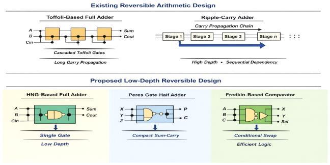
• Thecurrentdesignfeaturesaripple-carrystructureandafulladderbasedonToffoli.Thesum andcarryoutputs ofthe Toffoli-based completeadderare produced bycascading Toffoli gates. The carry signal spreadsstage by stageas a resultofseveralgatesbeingconnectedinsuccession.Highcircuitdepthandseveresequentialdependencyaretheresults of this extended carry propagation chain. Higher latency and more switching activity result from the depth increasing linearlywiththenumberofbits.
Furthermore,themajority ofcurrent researchanalyzes reversible circuitsusing staticcriteria suchgarbageoutputs,gate count,andquantumcost.Despitetheirsignificance,thesemeasuresfallshortindescribinghardware-levelperformancein CMOS-basedimplementations.Althoughswitchingbehaviorandpropagationdelayaredirectlyimpactedbycircuitdepth, depth is rarely considered the main optimization goal. Dynamic power consumption is increased when transitions are switchedacrossseveralcascadedstages,particularlyinworkloadsthataremostlyarithmetic-based.
Sequential control dependencies are also present in arithmetic logic units and comparator circuits built with FredkinandToffoligates.Cascadedcontrolstructuresarefrequentlyusedtoimplementconditionaloperations,increasing thelogicdepth.Whilesomearchitecturesprioritizefaulttoleranceandparitypreservation,theeffectofsuccessivelayering on switching energy is not thoroughly investigated. Therefore, structural organization rather than functional competence is the main drawback of current reversible arithmetic approaches. When operand size rises, cascaded architectures with universal gate dominance scale poorly in depth. Both quantum and CMOS-based reversible systems function less well when a systematic depth-minimization techniqueisnotused.
• Proposed Algorithm
For CMOS-based VLSI implementation, the suggested architecture presents a structured depth-optimized reversible arithmetic mapping mechanism. The main goal is to reduce the depth of the arithmetic circuit while maintaining computational accuracyand logical reversibility. The suggested method chooses reversible gates according on arithmetic functionaldensity,allowingseverallogicaloperationstobeincorporatedwithinasinglereversibletransformationstep,in contrasttotraditionalreversiblearithmeticdesignsthatpromoteuniversalgatedecomposition.
Themaximumnumberofsuccessivegatelayersencounteredalonganysignalpathfromprimaryinputtoprimary output is the formal definition of depth in reversible arithmetic circuits. A subset of the circuit's L reversible gate layers shouldbetraversedbyeachsignalpath.Themaximumpathlengthforeachinput-outputpairisthearithmeticdepthD.In quantum systems, when the length of circuit execution is constrained by the decoherence time, minimizing D directly lowersthepropagationdelayandsequentialdependency.
Arithmetic blocks are rearranged into compact reversible primitives in the suggested architecture. The main component needed to realize a full adder is the HNG gate. Several cascaded control procedures are used in traditional Toffoli-basedimplementationstogeneratethesumand carryoutputs.Sequentialdependencyisintroducedateachlevel, and depth increases linearly with operand size. On the other hand, the HNG gate combines AND-based carry generation and XOR-based sum computation into a single reversible mapping. The HNG gate lowers per-bit arithmetic depth to a singletransformationstagebyproducingbothoutputsatthesametime.
Likewise,thePeresgateisusedtocalculateintermediatecarrysignalsandpartialsumsinearly-stagearithmetic processes. The Peres gate's transformation is appropriate for half-adder and carry-merge functionality since it naturally integrates XOR andAND behavior.Intermediatecarry-onlylogiclevelsare removed by integrating bothoperationsinto a singlegate.Asaresult,fewercascadedstagesareneededoverallforaddition.
To reduce sequential reliance, the carry propagation mechanism is redesigned. The suggested architecture compresses carrycomputationwithinmultifunctionalgatesasanalternativetodependingonstrictlylinearripple-carrypropagation. Thearchitecturereducesthephysicalgatelayerswhilemaintaininglogicalripplerelianceforcorrectness.Asaresult,even when operand width rises, the maximum sequential gate depth drops. As a result, in contrast to conventional Toffolidominatedrippletopologies,theeffectivecriticalpathlatencyincreasesmoreslowly.
Threecompactarithmetic blocksaredepicted inthesuggested design: a Fredkin-basedcomparator, a Peres gate halfadder,andanHNG-basedfulladder.TheHNGgatereducesthenumberofcascadedstagesbygeneratingsumandcarry in a single reversible construction. By combining XOR and AND operations, the Peres gate allows for the creation of compact sum-carries using fewer logic levels. By carrying out conditional swap operations, the Fredkin gate reduces
International Research Journal of Engineering and Technology (IRJET) e-ISSN: 2395-0056
Volume: 13 Issue: 03 | Mar 2026 www.irjet.net p-ISSN: 2395-0072
control depth and streamlines comparator logic. This section emphasizes that, in comparison to the current cascaded structure,thesuggesteddesignachieveslowerdepth,fewersequentialsteps,andmoreeffectivearithmeticmapping.
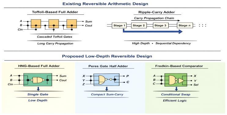
TheFredkingateisusedtoimplementcontrolledswapfunctionalityforcomparisonandconditionalselectionprocedures. Multiple cascaded control gates are frequently needed for conditional logic in traditional reversible comparators. The comparatordepthisdecreasedbydirectlyemployingcontrolledswapoperations.TheFredkingatecompressesthedepth ofcontrollogicbyenablingroutingdecisionswithoutaddingadditionalmultiplexingsteps.
There are several advantages to depth reduction from the standpoint of VLSI mapping. In CMOS implementation, each reversible gatelayerisequivalenttoa network oftransistors.Transistorstackingandparasiticcapacitanceaccumulation are increased by cascaded gate layers. The suggested architecture reduces effective capacitive loading along the critical pathbyloweringthenumberofsuccessivelayers.Thisenhancessignalintegrityandlowerspropagationdelay.Depthalso has a big impact on switching activity. Intermediate signals in cascaded systems may toggle even when the end outputs don’t change, which adds needless dynamic power dissipation. There are fewer intermediate switching nodes when arithmetic operations are embedded into single reversible units. This directly lowers energy consumption since dynamic power in CMOS circuits is proportional to switching activity. Reduced depth also improves stability in high-frequency operationbyloweringthelikelihoodofglitchpropagation.
A depth-aware gate selection technique is also included in the suggested architecture for mapping. The mapping frameworkrecognizesarithmeticpatternslikehalf-adder,full-adder,andconditionalroutingblocksandallocatesthemto Peres, HNG,orFredkingatesappropriately,ratherthan breakingdownBooleanarithmeticoperationsonlyinto universal gates.Gateselectionisguaranteedtobeinlinewithdepthminimizationgoalsand arithmeticfunctionalitythankstothis organized mapping. Scalability is a crucial factor to take into account. As the operand width increases, depth in traditional ripple-based reversible adders scales linearly. In the proposed design, although logical dependency remains, the compression of arithmetic operations within each stage reduces effective depth scaling. This leads to quantifiable gains in switching energy and delay for large operand sizes. Therefore, as mathematical complexity increases, the architecture gains more andmorebenefits.
Additionally,hybrid integrationwithadiabaticCMOS logicissupported bythesuggestedframework.Byrecyclingcharge throughout logic transitions, adiabatic approaches lower physical switching losses while reversible logic lowers information-loss energy. A dual-layer approach to energy reduction is produced by combining adiabatic switching with depth-optimized reversible gates. Practical dynamic power dissipation is minimized by adiabatic implementation, and theoreticalentropybuildupisminimizedbylogicalreversibility.ThedesignisgeneratedusingCMOStechnologylibraries andmodelledin HDL to verifyperformance gains.Incomparison to traditional CNOT/Toffoli-based architectures,critical pathdelay,gatecount,area usage,andpowerconsumptionareextracted.The evaluationframework providesa thorough performanceassessmentbymeasuringbothhardware-levelswitchingbehaviourandquantumcostequivalency.
International Research Journal of Engineering and Technology (IRJET) e-ISSN: 2395-0056
All things considered, the suggested design creates a methodical, arithmetic-focused reversible mapping approach that specifically focuses on VLSI efficiency and depth minimization. The design delivers lower switching activity, higher scalability, increased energy efficiency, and decreased critical route delay by choosing Peres, HNG, and Fredkin gates accordingtotheirarithmeticfunctionalityandswitchingbehavior.Becauseofthis,thearchitectureisespeciallywell-suited for low-power quantum-inspired computers, quantum simulators, quantum control circuits, and cryptographic accelerators.
• Results And Discussion
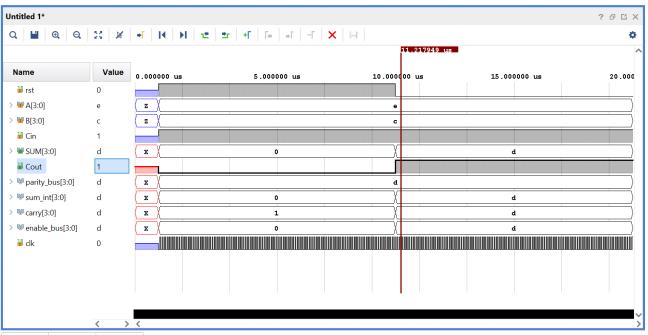
The designs are developedin Xilinx Vivado tool for the hardware ofchoice is 28nmCMOS technology basedArtix-7 FPGA board(xc7z020clg484-1).Thesystemrequirementsincludewindows10OS,4GBRAMinstalledwithXilinxVivado2023.2. Thesimulationresultofexistingandproposeddesignsareasshowninfig.3(a) &3(b).
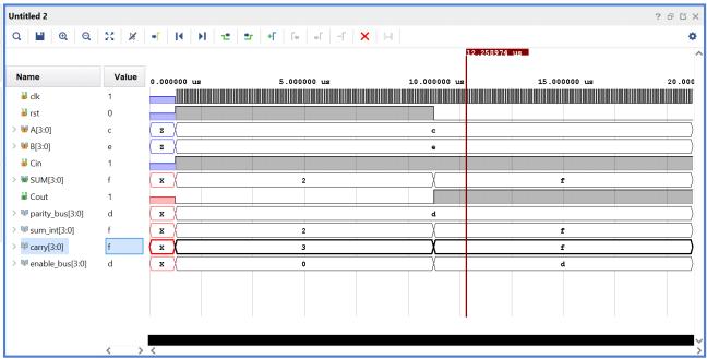
• Fig 3(b): SimulationresultofProposedDesign
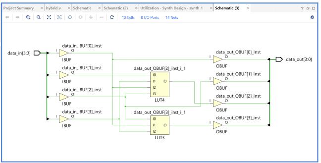
• Fig 4(a): TechnologySchematicofExistingdesign
Volume: 13 Issue: 03 | Mar 2026 www.irjet.net p-ISSN: 2395-0072 © 2026, IRJET | Impact Factor value: 8.315 | ISO 9001:2008 Certified Journal | Page1840
International Research Journal of Engineering and Technology (IRJET) e-ISSN: 2395-0056
Volume: 13 Issue: 03 | Mar 2026 www.irjet.net p-ISSN: 2395-0072
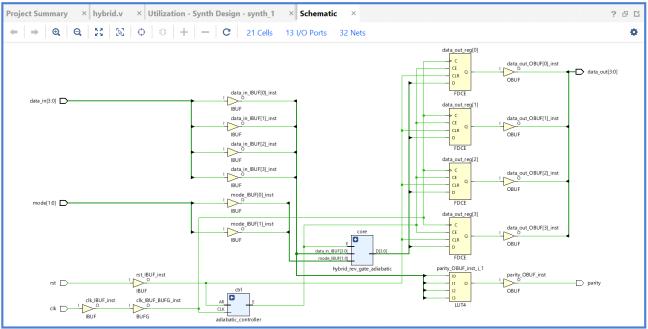
Fig 4(b): TechnologySchematicofProposeddesign
• Thetechnolgyschematicsofexistingandproposeddesignsareshowninfig.4(a)and(b)respectively.
• The circuit uses 10 logic cells, 8 I/O ports, and 14 nets, according to the technological diagram of the current designcreatedinXilinxVivado.Fourinputbuffers(IBUFs)connecttheinputsignals,andfouroutputbuffers(OBUFs)drive the outputs. LUT3 and LUT4 blocks, which realize the combinational logic obtained from traditional reversible gate operations, are used to implement the arithmetic logic. Several LUT stages are used in this approach to carry out the arithmetic operations. According to the technology diagram of the suggested design, the circuit makes use of 32 nets, 13 I/Oports,and21logiccells.IBUFsareusedtoconnectinputssuchdata,clock,reset,andmodesignals,whileaBUFGglobal clockbufferisusedtodistributetheclock.LUT-basedlogicblocksareusedtoimplementreversiblearithmeticoperations based on Peres, Fredkin, and HNG gates. OBUFs provide a more comprehensive and effective architecture for reversible arithmeticimplementationbydrivingtheoutputs,whichincludedataandparitysignals.
• According to the comparison results, the suggested reversible gate architectureoutperforms the current designintermsofperformance.Alowerarithmeticdepthisshownbythemaximumpropagationdelaybeingloweredfrom 7.029nsto6.935ns.Additionally,thereisanimprovementinenergyefficiencyastheoverallon-chippowerusagedrops from 1.605 W to 1.278 W. Additionally, the junction temperature drops from 43.5 °C to 39.7 °C, indicating improved thermal properties. These enhancements confirm that the suggested reversible arithmetic architecture based on PeresFredkin-HNG offers a more effective VLSI implementation appropriate for low-power quantum-inspired computing systems.
Table 1:comparisonamongexistingandproposeddesigns
International Research Journal of Engineering and Technology (IRJET) e-ISSN: 2395-0056
Volume: 13 Issue: 03 | Mar 2026 www.irjet.net p-ISSN: 2395-0072
Conclusion
Inthispaper,aVLSIimplementationofreversiblegatesforlow-depthquantumarithmeticwasprovided.Toobtainamore effective arithmetic realization, the suggested architecture makes use of Peres, Fredkin, and HNG gates rather than traditional CNOTand Toffoligates. The suggestedarchitecturelowers the propagationlatency from7.029 ns to 6.935 ns, the total on-chip power from 1.605 W to 1.278 W, and the junction temperatureto 39.7 °C, according to implementation results in Xilinx Vivado. These enhancements show that the suggested reversible logic design offers a more effective and energy-efficientsolutionforVLSIarithmeticsystemsinspiredbyquantummechanics.Inordertofurtherminimizepower consumption for scalable quantum and edge computing hardware, future work can extend this design to complicated arithmeticunitslikemultipliersandALUsandinvestigateadiabaticCMOSandsophisticatedreversiblegatelibraries.
References
1. Kanchan S. Tiwari1 , Rekha S. Kadam1 , Manisha A. Dudhedia2 , Jayshree R. Pansare3 , Shilpa P. Khedkar3 , Shravan H. Gawande, “Reversible Logic Gates and Applications – A Low Power Solution to VLSI Chips” https://doi.org/10.18280/mmep.110315
2. .S. Nagaraj, B. V. Krishna, B. Chakradhar and D. Sarkar, "Comparison of 32-bit ALU for Reversible Logic and IrreversibleLogic,"2021InnovationsinPowerandAdvancedComputingTechnologies(i-PACT),KualaLumpur, Malaysia,2021,pp.1-5,doi:10.1109/i-PACT52855.2021.9696935.
3. S.Vijayashaarathi,V.Tamilselvam,K.Saranya,J.HarirajkumarandL.Satheeskumar,"OptimizedArithmeticand Logical Unit Design using Reversible Logic Gates,"2023 2nd International Conference on Applied Artificial Intelligence and Computing (ICAAIC), Salem, India, 2023, pp. 1597-1603, doi: 10.1109/ICAAIC56838.2023.10140400.
4. G. Chandran, H. M. M. C and A. G, "VLSI Implementaion of Image Encryption and Decryption Using Reversible Logic Gates,"2020 International Conference on Power Electronics and Renewable Energy Applications (PEREA),Kannur,India,2020,pp.1-6,doi:10.1109/PEREA51218.2020.9339781.
5. S. M. Bhat and V. Kakkar, "Design and Modeling of an Ultra-Efficient 3x3 SSG-1 Reversible Gate for Nanoscale Applications,"2021 International Conference on Emerging Smart Computing and Informatics (ESCI), Pune, India,2021,pp.720-723,doi:10.1109/ESCI50559.2021.9397042.
6. K. Yashoda, K. V. Gowreesrinivas, M. U. Mahesh, K. S. V. L. D. S. Phanindra, A. Syed and S. Sai, "Design And Implementation Of Power Efficient Multiplier Using Reversible Logic,"2025 Devices for Integrated Circuit (DevIC),Kalyani,India,2025,pp.390-395,doi:10.1109/DevIC63749.2025.11012388.
7. A.V.SandA.Chalil,"FPGAImplementationofCryptographyUsingReversibleLogicGatesforImages,"20233rd Asian Conference on Innovation in Technology (ASIANCON), Ravet IN, India, 2023, pp. 1-6, doi: 10.1109/ASIANCON58793.2023.10270197.
8. R. Pandimeena, S. Aathilakshmi, D. M. Vaheen, H. Vijay, M. K and B. S. A. S, "FPGA Implementation of Normal Basis Multiplier Using Reversible Logic,"2024 10th International Conference on Advanced Computing and Communication Systems (ICACCS), Coimbatore, India, 2024, pp. 1688-1694, doi: 10.1109/ICACCS60874.2024.10716911.
9. J. Nessa, S. Dash and M. C. Tripathy, "High Speed Low Power 16×16 Dadda Multiplier by Utilizing Reversible Gates,"2025 IEEE 5th International Conference on VLSI Systems, Architecture, Technology and Applications (VLSISATA),Bangalore,India,2025,pp.1-5,doi:10.1109/VLSISATA65374.2025.11070214.
International Research Journal of Engineering and Technology (IRJET) e-ISSN: 2395-0056
Volume: 13 Issue: 03 | Mar 2026 www.irjet.net p-ISSN: 2395-0072
10. B. Gaur, T. S. Humble and H. Thapliyal, "Residue Number System (RNS) Based Distributed Quantum Addition,"2024IEEEComputerSocietyAnnualSymposiumonVLSI(ISVLSI),Knoxville,TN,USA,2024,pp.595600,doi:10.1109/ISVLSI61997.2024.00113.
11. H.T.Larasati,D.S.C.Putranto,R.W.Wardhani,J.ParkandH.Kim,"DepthOptimizationofFLT-BasedQuantum InversionCircuit,"inIEEEAccess,vol.11,pp.54910-54927,2023,doi:10.1109/ACCESS.2023.3280632.
12. Y. Zhu, R. Yang, Y. Gu, F. Gu, L. Kong and H. Li, "Towards Fault-tolerant Design of Quaternary Quantum Arithmetic,"2024 IEEE International Test Conference in Asia (ITC-Asia), Changsha, China, 2024, pp. 1-6, doi: 10.1109/ITC-Asia62534.2024.10661353.
13. H.Thapliyal,E.Munoz-CoreasandV.Khalus,"SpecialSession:QuantumCarryLookaheadAddersforNISQand Quantum Image Processing,"2020 IEEE 38th International Conference on Computer Design (ICCD), Hartford, CT,USA,2020,pp.5-8,doi:10.1109/ICCD50377.2020.00014.
14. F. Zonzini, N. Testoni, A. Marzani and L. de Marchi, "Low Depth Time Reversal Modulation Technique for Ultrasonic Guided Waves-based Communications,"2020 IEEE International Ultrasonics Symposium (IUS), Las Vegas,NV,USA,2020,pp.1-4,doi:10.1109/IUS46767.2020.9251321.
15. Y. Baumann, T. Ben-Nun, M. Besta, L. Gianinazzi, T. Hoefler and P. Luczynski, "Low-Depth Spatial Tree Algorithms,"2024 IEEE International Parallel and Distributed Processing Symposium (IPDPS), San Francisco, CA,USA,2024,pp.180-192,doi:10.1109/IPDPS57955.2024.00024.
16. B. G. Bach, F. B. Maciejewski and I. Safro, "Solving Large-Scale QUBO with Transferred Parameters from Multilevel QAOA of Low Depth,"2025 IEEE International Conference on Quantum Computing and Engineering (QCE),Albuquerque,NM,USA,2025,pp.2120-2126,doi:10.1109/QCE65121.2025.00232.