International Research Journal of Engineering and Technology (IRJET) e-ISSN: 2395-0056

Volume: 09 Issue: 09 | Sep 2022 www.irjet.net p-ISSN: 2395-0072
International Research Journal of Engineering and Technology (IRJET) e-ISSN: 2395-0056
Volume: 09 Issue: 09 | Sep 2022 www.irjet.net p-ISSN: 2395-0072
 Spandana S D1 , Dr. Kiran Bailey
2
1M. Tech Scholar, Dept of ECE, BMSCE, Bengaluru, Karnataka, India
2 Assistant Professor, Dept. of ECE, BMSCE, Bengaluru, Karnataka , India ***
Abstract - Optimizing the power consumption of flip-flops (FFs) can greatly lower the power consumption of digital systems. An energy-efficient retentive true single-phaseclocked (TSPC) FF is proposed . The proposed TSPC FF precharges only when necessary by using input-aware precharge strategy. Floatingnodeanalysis andtransistor level optimization are also used to assure the FF's great energy efficiency without considerablyexpandingits size. Byusing22nm CMOS technology, the suggested FF consumes 30.37 percent less power than a standardtransmission-gateflip-flop (TGFF) at 10% data activity at a supply voltage of 0.95 V. As the data activity decreases to 0%, the reduction rateincreases to 98.53 percent.
Key Words: Flip flop, low voltage operation, low power, redundant-precharge-free,truesinglephaseclocked(TSPC).
Astheprocesshasadvanced,digitalsystems'performance has significantly improved, and power consumption has turnedintoaseverelimitation.Additionally,IOTdevicesare widelyusedintheInternetofThingsduetothe Internet's explosive growth (IOT). There are several uses for the Internet of Things (IOT). Just a few examples include transportation, healthcare, and intelligent settings. Such battery-powered or self-powered devices use low-power components. Flip-flops (FFs) are key components that account for a sizeable amount of the total power. FFs frequentlyconsume50%ormoreofthepowerconsumed for operations in the random logic sector. Due to its redundanttransitionofinternalnodeswhentheinputand output are in the same state, flip-flops (FF) generally consumemorethanhalfoftherandom-logicpowerinaSoC device.HenceloweringthepowerconsumptionofFFscan drastically minimize the amount of energy consumed by Digitalsystems.
The transmission-gate flip-flop (TGFF) is the FF that is utilizedthemostfrequentlyinmoderndigitalsystems.The TGFFschematicisdepictedinFigure1.TheTGFFisanear thresholdoperation-capable,contention-freeFF.Thebiggest problem with TGFF is the extensive clock network. The internalnodesCKNandCKItoggle,andthenodesCKNand
CKIdriveagreaternumberoftransistors,regardlessofthe inputdata.Asaresult,TGFFcontinuestoconsumealotof power even when data traffic is minimal. To reduce FF's powerusage,complementaryclocksignalsshouldbeused moreselectively.
Fig -1:SchematicofDflipflopusingtransmissiongate
Previous publications [2]–[6] have proposed many lowpower single-phase-clocked FFs. However, there are still certainissueswiththepowerusageoftheseFFs'.SomeFFs, failatlowsupplyvoltage[2]–[4],[6],andothershaveahigh precharge power [2], [4]–[6]. This article proposes a lowpowertrue-single-phase-clocked(TSPC)FF.Thesuggested FFisfreeofcontentionandcanoperateatawiderangeof supply voltages. Furthermore, in comparison to previous low-power FFs, redundant precharge operation is completely eliminated in the proposed FF, and power consumptionisfurtherminimized
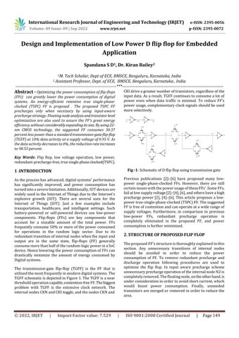
TheproposedFF'sstructureisthoroughlyexplainedinthis section. Any unnecessary transitions of internal nodes should be avoided in order to reduce the power consumption of FF. To remove redundant precharge and discharge operation following procedures are used to optimize the flip flop. In input aware precharge scheme unnecessaryprechargeoperationoftheinternalnodeN2is completelyremoved.Thefloatingnode,ontheotherhand,is underconsiderationinordertoavoidshortcurrent,which would boost power consumption. Finally, unneeded transistorsare mergedorremovedinordertoreduce the area
International Research Journal of Engineering and Technology (IRJET) e-ISSN: 2395-0056
Volume: 09 Issue: 09 | Sep 2022 www.irjet.net p-ISSN: 2395-0072
throughM14(D=0),N1isisolatedfromitspull-downpath (M13andM14),andthevoltageofN2hasnoeffectonthe nodeN1.Asaresult,thefloatingofnodeN2isinsignificant inthiscase.
Theredundantprechargeoperationiseliminatedafterusing the input-aware precharge scheme and floating node analysis, but the FF can be improved further. M11 can be merged with PMOS M11 1, which is used to generate the inversionoftheinputdata.However,theNMOSM15cannot becombinedwithM14atthesametime.WhenbothPMOS and NMOS are merged, the drains of M11 and M14 are directlyconnected,whichcanresultinFFfunctionalfailures. Asaresult,theNMOSM15isreserved,asillustratedinFig.2.
Whentheinputdatais0,theprecharging ofthenodeN2is not necessary, hence the precharge path should be cutoff when D =0..APMOSM1thatiscontrolledbytheinputdata isinvertedandinsertedintotheprechargepathofflipflop.. If the input data is a 1, PMOS M1 is turned on, and the necessaryprechargeoperationworksasexpected.Whenthe inputdataremainszero,thePMOSM1isturnedoff,andthe precharge path is blocked by the inserted transistor. As a result, the redundant precharge operation is no longer required.
Floatingnodesneedtobecarefullyanalyzedsinceleakage current during transition may cause their voltage to fluctuate,whichcould leadtotheformationofshort-circuit routes.ThevoltageofthenodeN2isnolongerprechargedto VDDatthenegativehalfcycleofCKwhentheinputiszeroas a result of the installation of input aware transistors. The stateofthenodeN2mustthereforebecarefullyexamined
Transistor M9 and M10 retain the state of N3 when the outputQ=1,whichresultsinN3=0.ThevoltageofN2must behighinordertomaintainthetransistorM3OFFandthe transistorM10ONatthatmoment.AtransistorM2isplaced tomaintainthevoltageofN2inordertopreventN2from floatingwhilethefollowinginputdatais0.WhenQ=1,N2 hasaprechargechannelthroughM2,whichiscontrolledby N3.
TransistorM7andM8retainN3'sstatewhentheoutputQis equal to 0. When clk is low and input data is 0 precharge pathofN2iscutoffandhencevoltageofN2doesn’tcharge tohigh.ThenodeN3isisolatedfromitspull-downpath(M4 andM5)throughM4whenN3=1,CK=0,andD=0,hence thevoltageofN2hasnoimpactonthenodeN3. Similarly,
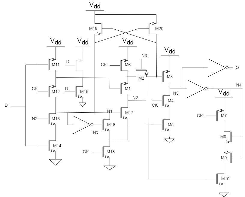
ThedetailedoperationoftheproposedFF isshowninFig.3.
When CK is low, nodes N1 and N2 are charged to VDD through M11-M12 and M6-M2 respectively. Node N3 maintainsalowstatethroughM9andM10,andtheoutputQ remains high. To isolate the FF from changes in the input data, M13 is turned off after N2 is discharged to GND throughM17andM18attherisingedgeofCK.TheoutputQ goesto0oncethenodeN3ischargedtoVDD throughM3. ThroughoutthepositivehalfcycleofCK,N1maintainsahigh voltagethroughM19,whereasN2maintainsalowvoltage throughM17andM18.
WhenCKislow,thenodeN3maintainsahighstatethrough M7andM8,N2ischargedtoVDDthroughM6andM1,N1is discharged toGND through M13and M14,andthe output maintainsalowstatethroughM7andM8.ThenodeN3is dischargedtoGNDthroughM4andM5andtheinputdatais
2022, IRJET | Impact Factor value: 7.529 | ISO 9001:2008 Certified Journal |
International Research Journal of Engineering and Technology (IRJET) e-ISSN: 2395-0056
Volume: 09 Issue: 09 | Sep 2022 www.irjet.net p-ISSN: 2395-0072
isolatedthroughM12attheCKrisingedge,afterwhichthe outputQswitchesto1.DuringthepositivehalfcycleofCK, thevoltageofN1remainslowthroughM16andM18while thevoltageofN2remainshighthroughM20.
FFsgenerallyneedextrafeatureslikeset,reset,andscanin digitalsystems.TheproposedFFcansimplybeexpandedto includetheseextrafeatures.
Fig -4:SchematicoftheproposedFFwithset
Fig 4 shows the schematic of proposed flip flop with set. WhenSNislowandSETishighthechargingpathofN1is blockedbyM21,andN1isdraggeddownthroughM22.N2is chargedtoVDDthroughM20becausethe nodeN1islow. N3'schargingpathisblockedbyM23atthesametimethat N3ispulleddownbyM24andtheoutputremainshigh.The transientwaveformofthesuggestedFFwithasetfunctionis showninFig.4.1.Asseenin Fig.4.1,theoutputQremains highwhileSNislow,indicatingthattheFFisinthesetstate. On the other hand, the FF functions normally when SN is high.
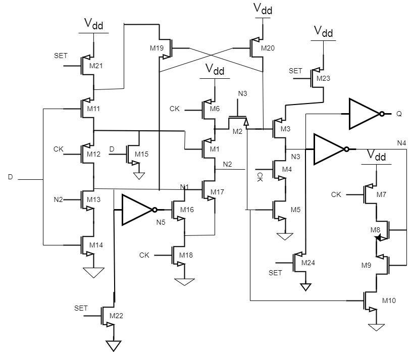
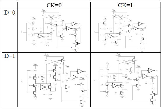
TheproposedFFwithresetfunctionisshownschematically inFig.5whentheresetsignalRSTNislowandRSTishigh thechargingpathofN2isblockedbyM21,andN2isdragged downthroughM22,asshowninFig.4.2.N3ischargedtoa high level through M3 since N2 is low, and the output Q remainslow.N1ischargedtohighthroughM19atthesame time WhenCK=0andD=1,aPMOSM23isintroducedto isolateN1fromtheinputandpreventshortcircuitcurrent throughM12andM15.
The transient waveform of the suggested FF with reset function is shown in Fig. 5. As seen in Fig. 5 the output Q remainslowwhenRSTNislow,indicatingthattheFFisin theresetstate.Incontrast,theFFsuccessfullycollectsthe inputdataattherisingedgeofCKwhenRSTNishigh.
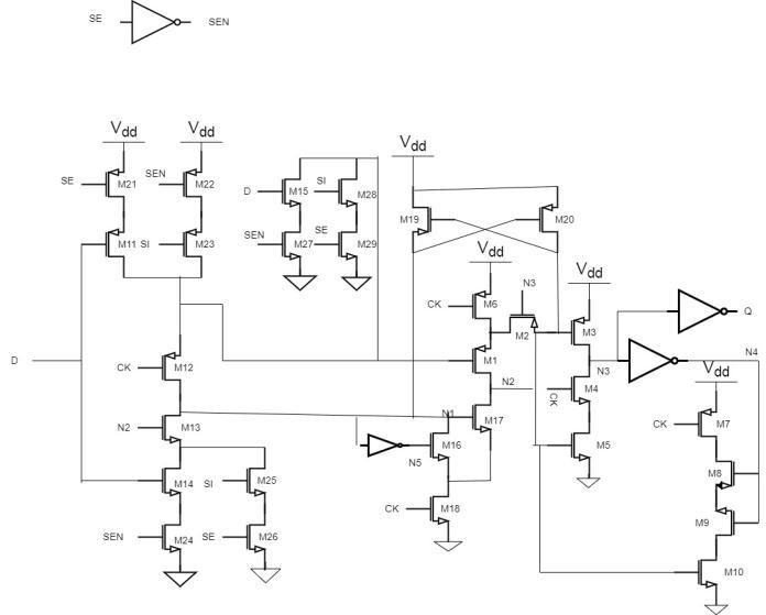
The proposed FF with the scan function is shown schematicallyinFig.6.AsseeninFig.6,theinputdata D is separated from the FF when the scan enable signal SE is high,andtheFFcapturesthedataofthescaninputSIatthe rising edge of CK. The FF catches the input data D at the risingedgeofCKwhenSEislow,isolatingSIfromtheFF.
Simulation using 22-nm CMOS is used to show the performanceofProposedFF.Forthesimulation,thesame transistorsizeisused.TheproposedFFcanoffersignificant
International Research Journal of Engineering and Technology (IRJET) e-ISSN: 2395-0056
Volume: 09 Issue: 09 | Sep 2022 www.irjet.net p-ISSN: 2395-0072
energyefficiencyimprovementswhenappliedtolarge-scale integratedcircuits,whichisduetotheremovalofredundant prechargeoperations,asdescribedin[4],whichstatesthat the average data activity of FFs in large-scale integrated circuitsistypicallybetween5and15percent.Innearlyall areasofdataactivity,ProposedFFusestheleastamountof power.
Power comparison of proposed FF and TGFF at different technologynodeislistedintable1.Hereanalysisisdonefor 180nm, 45nm, 32nm and 22nm CMOS technology node. Power dissipation keeps on decreasing as we move from highertechnologynodetolowertechnologynodeandpower dissipationofproposedFFislesscomparedtoTGFFinevery technologynode.
At10%dataactivity,thepowerdissipationofproposedFFis 66%lowerthanthatofTGFF.Similarlyat0%dataactivity the power dissipation of proposed FF is 98% lower than TGFF whichislistedintable2. TheproposedFF uses only 1.5%ofthepowerusedbytheTGFFwhendataactivityis zero. This is mostly due to the fact that the proposed FF requires no additional operations while there is no data activity,hencetheonlypowerconsumptionatthistime is leakage power. When the data activity for TGFF is 0, the internalnodes(CKNandCKI)stillneedtofunctionasusual, wastingalotofpower.
Technology Parameters Transmission gateFF Proposed FF
22nm Power 1.0519E-07 7.4683E-08 Delay 4.0628E-09 4.0617E-09
32nm Power 1.9822E-07 1.6852E-07 Delay 4.0886E-09 4.0536E-09
45nm Power 3.8184E-07 2.6824E-07 Delay 4.0936E-09 4.0559E-09
180nm Power 4.1599E-05 2.5956E-05 Delay 4.1940E-09 4.0793E-09
Table 1: Comparisonofpoweranddelayatdifferent technologynode
Precharge and discharge processes are still required for otherFFssuchtheSPC-18TFFandS2CFFwhilethedatais still0,whichindicateslesserenergyefficiencycomparedto theproposedFF.InACFFandTCFF,thereisnoredundant prechargeprocess,andbothtypesofFFsexhibitgoodenergy efficiencywhenthereisnodataactivity.However,thetwo FFs'powerincreasesmorequicklywithdataactivitydueto currentcontention(inACFF)andalargenumberofshared transistors(inTCFF),whichlowerstheirenergyefficiency.
FlipFlop Transmission gateFF Proposed FF
AveragePowerwhen dataactivityis10% 1.0519E-07 7.4683E-08
AveragePowerwhen dataactivityis0% 5.1698E-08 5.9309E-10
Table 2: Comparisonofpoweratdifferentdataactivity
An energy-efficient retentive TSPC FF is proposed in the paper. The input-aware precharge approach considerably reduces the power of the proposed FF by eliminating superfluous precharge and discharge procedures. The proposedstructureisalsosubjectedtofloatingnodeanalysis topreventtheformationofshort-circuitroutes.Thecircuitis thenoptimizedatthetransistorleveltofurtherreduceits sizeandpowerusage.Accordingtopostlayoutsimulation results, the suggested FF consumes less power than TGFF withlessthan10%dataactivity.
[1] Heng You Jia Yuan, Zenghui Yu “Low-Power Retentive True Single-Phase-Clocked Flip-Flop With RedundantPrecharge-FreeOperation,”IEEETRANSACTIONSONVERY LARGESCALEINTEGRATION(VLSI)SYSTEMS,VOL.29,NO. 5,MAY2021
[2]A.Hirata,K.Nakanishi,M.Nozoe,andA.Miyoshi,“The crosschargecontrolflip-flop:Alow-powerandhigh-speed flip-flopsuitableformobile applicationSoCs,”in Dig. Tech. Papers. Symp. VLSI Circuits,Jun.2005,pp.306–307.
[3] C. K. Teh, T. Fujita, H. Hara, and M. Hamada, “A 77% energy-saving22-transistorsingle-phase-clockingD-flip-flop with adaptive-coupling configuration in 40 nm CMOS,” in IEEE Int. Solid-State Circuits Conf. (ISSCC) Dig. Tech. Papers, Feb.2011,pp.338–339.
[4]N.Kawai et al.,“Afullystatictopologically-compressed 21-transistorflip-flopwith75%powersaving,” IEEEJ. SolidState Circuits,vol.49,no.11,pp.2526–2533,Nov.2014.
[5]Y.Cai,A.Savanth,P.Prabhat,J.Myers,A.S.Weddell,and T.J.Kazmierski,“Ultra-lowpower18-transistorfullystatic contention free single-phase clocked flip-flop in 65-nm CMOS,” IEEE J. Solid-State Circuits,vol.54,no.2,pp.550–559, Feb.2019.
[6] Y. Kim et al., “A static contention-free single-phaseclocked24Tflipflopin45nmforlow-powerapplications,” in IEEE Int. Solid-State Circuits Conf. (ISSCC)Dig. Tech. Papers, Feb.2014,pp.466–467.
2022, IRJET | Impact Factor value: 7.529 | ISO 9001:2008 Certified Journal |
International Research Journal of Engineering and Technology (IRJET) e-ISSN: 2395-0056
Volume: 09 Issue: 09 | Sep 2022 www.irjet.net p-ISSN: 2395-0072
[7]F.StasandD.Bol,“A0.4-V0.66-fJ/cycleretentivetruesingle-phaseclock18Tflip-flopin28-nmfully-depletedSOI CMOS,” IEEE Trans. Circuits Syst. I, Reg. Papers,vol.65,no.3, pp.935–945,Mar.2018
2022, IRJET | Impact Factor value: 7.529 | ISO 9001:2008 Certified Journal