International Research Journal of Engineering and Technology (IRJET) e-ISSN:2395-0056

Volume: 09 Issue: 09 | Sep 2022 www.irjet.net p-ISSN:2395-0072
International Research Journal of Engineering and Technology (IRJET) e-ISSN:2395-0056
Volume: 09 Issue: 09 | Sep 2022 www.irjet.net p-ISSN:2395-0072
E.Ritheesh1, P.Pugazhendiran2, R.Revathy3
1Graduate, Dept. of EEE, IFET college of Engineering, Tamilnadu, India
2Professor, Dept. of EEE, IFET college of Engineering, Tamilnadu, India
3Assistant Professor, Dept. of EEE, IFET college of Engineering, Tamilnadu, India ***
Abstract - When it comes to sustainable energy, solar photovoltaic energy production is crucial. The photovoltaic cells use a portion of the sun's energy, which is copious and readily available. Therefore, the energy conversion mechanism should have great efficiency. Consequently, a high-efficiency dc-dc converter for low-voltage solar sources is suggested. Great voltage gain and high efficiency are used by the suggested converter to increase DC voltage. Dual active clamping circuits and a resonant voltage doubler rectifier are used in the proposed converter. Power switches experience less voltage stress on the low voltage side. Output diodes can be turned off with zero current on the highvoltage side.
Key Words: Photo - voltaic (PV), power efficiency DC-DC converter.
The primary technology for future solar-powered electricity production is the photovoltaic (PV) moduleintegrated converter (MIC) system [4], [5]. There is a unique power conversion system for every PV module. The PV module's maximum power is produced via the power conversion system [7]. A high-efficiency and inexpensivepowerconversionschemeneedstobecreated in order for the PV MIC system to be economically viable. The PV module often exhibits a low-voltage characteristic [15].Lowvoltage(thedcvoltageofaPVmodule)mustbe converted into high voltage in order to supply electricity to the grid [14]. A high-voltage gain dc-dc converter is thereforerequired.
The integrated cascade boost converter's switch voltage stress is equal to high voltage, and the current stress is significant [1]. Conduction losses go up and the converter's efficiency goes down with a cascade boost converter. By increasing the coupled inductor's turns ratio, a converter with a coupled inductor can simply increase its voltage gain. It does, however, have a sizable steady-state inductance. The overall efficiency is decreasedasaresultofthelargesteadystateinductance's increased losses [12]. The converter layout is also intricate, and the design process is as difficult. The magnetic components, such as the inductor or the transformer,won'tbeneededfortheSCconverters.Thus,
a high amount of switching frequency can be achieved. However,inordertoobtainhigh-voltagegain,morepower components are needed, which raises the converter's complexityandprice[6].
Due to their components inability to withstand high powercircumstances,themajorityofsingle-phaseisolated DC/DC converters appear inadequate and deficient. The losses of the converter rise as the phase shift does in a multiphase dual active bridge converter. Additionally, the design uses two switch legs, which means that a threephase converter needs 12 power switches, increasing the numberof switches,switchinglosses,andconverter price [10]. Due to its high leakage inductance (0 D 0.333), the MultiphaseZVSPWMDC/DCConverterhasalimitedduty cycle and experiences high circulating energy in the main sideduringfree-wheelingperiods[3].
Photovoltaic sources have made use of the active-bridge dc-dc converter [9], [2]. At zero voltage, the power switches on the low-voltage side are activated. However, due to its reverse-recovery current, the output diode on the high-voltage side suffers from significant switching powerlosses.Tolessenswitchingpowerlossesatthehigh voltage side, the half-bridge dc-dc converter has been introduced [16]. By using a voltage doubler rectifier circuit, the output diodes are turned off at zero current. However,thisrequiresasecondhalf-waverectifier,which raises switching power losses. As an alternative, lowvoltage PV sources have been employed with activeclamped dc-dc converters [8], [13]. It makes use of the resonant voltage doubler rectifier and active-clamping circuits.
For low-voltage PV sources, a high-efficiency dc-dc converteris suggested in thisresearch.By utilising a dual active-clampingcircuit,anactive-clampeddc-dcconverter isprovided.Onthelow-voltageside,thevoltagestress on power switches is lessened. The suggested converter's operation is described. The PSIM programme is used to confirm the proposed converter's performance. The simulationresultsdemonstratethatat41-Vvoltagesource for330-Woutputpower,ahighefficiencyof98percentis attained.
International Research Journal of Engineering and Technology (IRJET) e-ISSN:2395-0056
Volume: 09 Issue: 09 | Sep 2022 www.irjet.net p-ISSN:2395-0072
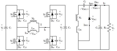
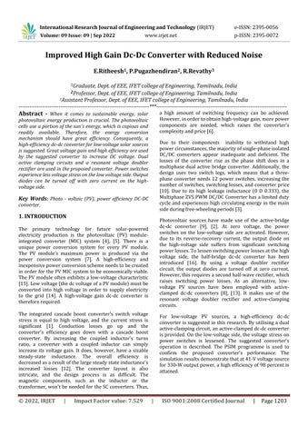
Fig. 1 depicts the proposed DC/DC converter with a voltagedoublerrectifieranddualactiveclampingcircuits. TheDC/DCconverterthatisbeingsuggestedisanAClink chopper. Dual active clamping circuits were used to make the inverter part. The rectifier part employs a resonant voltage doubler rectifier. The dual active-clamping circuit (S2, S3, Cc), transformer T, and resonant voltage doubler rectifier are the major switches (S1, S4) in the proposed DC/DCconverter(Llk ,Cr ,Do1 ,Do2 ).Withlittledeadtime, theprimaryswitches(S1,S4)andauxiliaryswitches(S2,S3) aredesignedtoworkintandem.
Metal-oxide semiconductor field-effect transistors are usedineachswitch.ExceptfortheiroutputcapacitorsCS1–CS4 and body diodes DS1– DS4, they are regarded as ideal switches. The input capacitor's name is Ci The clamping capacitor is Cc. The output capacitor is named Co ThevoltagesVi,Vc,andVo ofthecapacitorsCi,Cc andCo are each large enough to be regarded as constants. The transformer has a leaking inductor Llk and a magnetising inductorLm.Llk isthoughttobesomewhatsmallerthanLm Thetransformerhasaturnsratioof1:N,whereN=Ns/Np. TheresonantcapacitoriscalledCr
(= CS1= CS2=CS3=CS4) is so small. S1 and S4 are turned ON oncemoretostartthenextswitchingcycle.
Fig. 1: showstheproposedDC-DCconverter'scircuit diagram.
The suggested DC-DC converter's switching waveforms are shown in Fig. 2 for one switching period Ts =(1/fs). Figure displays the switching waveforms at the primary side (a). The switching waveforms at the secondary side are depicted. Six switching modes are available in the proposed DC/DC converter during Ts. The main switches' on-time provides the basis for the duty ratio D. S2 and S3 have been deactivated prior to t = t0. When the principal currentiptravelsthroughthebodydiodesDS1 andDS4,the voltagesVS1 andVS4 havebeenzero.
Thetimeintervalduringthismodeisregardedasminimal incomparisontoTs becausetheswitchoutputcapacitorCS
2.3.
The inductor volt-second balancing principle states that the average value, or dc component, of voltage supplied across an ideal inductor winding must be zero. This idea also holds true for every transformer winding and other magneticdeviceswithnumerouswindings.
The voltages Vc and Vr are expressed as a result of the voltage-second balance relation on the magnetising inductorLm
Vc =[D/(1-D)]Vi
Vr =(1-D)Vo
The output voltage Vo and the input voltage Vi are obtained using thevoltage-second balance relation on the secondarywindingofTduringTs
Vo/Vi =N/(1-D)
TheinputvoltageVi regulatesthemaximumvoltagestress of S1 and S3. The clamping capacitor voltage Vc is the maximum voltage stress that S2 and S4 can withstand. Figure4depictstherelationshipbetweenthedutyratioD and the clamping capacitor voltage Vc. The inverter portion ofthesuggestedDC/DCconverter employs a dual active-clampingcircuit.Whenusingadualactive-clamping circuit, the clamping capacitor voltage is always lower thanwhenusingatraditionalactive-clampingcircuit.
By adopting the traditional active-clamping circuit, it means that the switch voltage stress of the proposed DC/DC converter is consistently lower than the switch voltagestressofthepreviousconverter[12].
The clamping capacitor voltage Vc may be lower than the input voltage Vi, particularly when the duty cycle ratio is less than 0.5. It is especially helpful in low-voltage PV systems where switching power losses account for more thanhalfofthetotalpowerlosses.
Before turning ON the output diodes Do1 and Do2, the currentsviatheoutputdiodesiDo1 andiDo2 shouldbezero. Before the output diode is turned OFF, the series resonance in Mode 1 and Mode 4 should have completed its half-resonant time. For the output diodes to be turned off at zero current, the following requirements must be met.
International Research Journal of Engineering and Technology (IRJET) e-ISSN:2395-0056
Volume: 09 Issue: 09 | Sep 2022 www.irjet.net p-ISSN:2395-0072
Sin[ωcDmaxTS] =0 ifDmax ≤0.5
Sin[ωc (1-Dmax )TS]=0 ifDmax >0.5
Theresonantfrequency, fr,shouldbegreaterthanthecriticalresonantfrequency, fc,toenablezero-currentturnoffoftheoutputdiode.
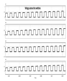
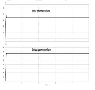
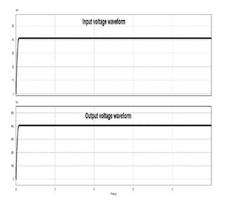
Table- 1lists thespecificationsof thevariouspartsthat make up the suggested DC/DC converter. A triangle and DCsignaliscomparedinordertoapplythegatingsignals to the gate terminal of the power switches. We may obtain equal-distance PWM pulses by comparing these twosignals,andthesepulsesarethenappliedtothegate terminals of the power switches S1 to S4. Figure 6 displays the voltage across the switches. The input and output voltage simulation waveforms are displayed in Fig. 6. 41 volts is the typical input voltage. 409V is the average output voltage as measured. The input and output power waveforms are displayed in Fig. 6. About 337Wistheinputpower.A330Waverageoutputpower has been determined. The difference between the input and output powers is minimal. Thus, the suggested DCDCconverterachieveshighvoltagegainandefficiencyof 97.9%.
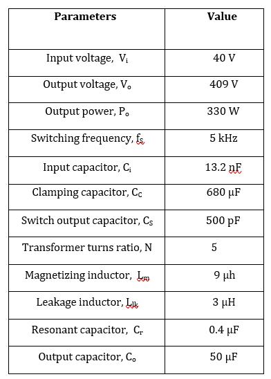
Fig. 2: shows the relationship between the clamping capacitor voltage Vc and the duty ratio D: (a) in the scenario of the traditional active-clamping circuit, and (b) inthescenarioofthedualactive-clampingcircuit.
The simulation results are given using PSIM 9.0 software tosupportthetheoreticalstudyofthesuggestedtopology.
Table -1: SimulationParameters
Fig. 3: shows the waveforms of the gate voltage (Vg1 & Vg2),theDCsignal(Vdc),andthecarriervoltage(Vtri)
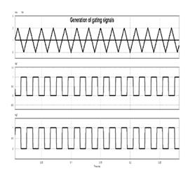
Fig. 4: Voltagewaveformsoverswitches (Vs1,Vs2,Vs3 & Vs4)
International Research Journal of Engineering and Technology (IRJET) e-ISSN:2395-0056
Volume: 09 Issue: 09 | Sep 2022 www.irjet.net p-ISSN:2395-0072
prototypes could be produced with high gain and great efficiency.
[1] B.Liu,S.Duan,andT.Cai,“PhotovoltaicDC-buildingmodule-based BIPV system: Concept and design considerations,”IEEETrans.PowerElectron.,vol.26, no.5,pp.1418–1429,May2011.
[2] C.RodriguezandG.A.J.Amaratunga,“Long-lifetime power inverter for photovoltaic ACmodules,” IEEE Trans. Ind. Electron., vol. 55, no.7, pp. 2593–2601, Jul.2008.
Fig. 5: Waveformsofinputandoutputvoltage(Vin,Vo)
[3] D.deSouza Oliveira, Jr. and I.Barbi,"A three- phase ZVS PWM DC/DC converter with asymmetrical duty cycle for high power applications," IEEE Transactions on Power Electronics, vol. 20, pp. 370377,2005.
[4] E. Serban and H. Serban, “A control strategy for a distributed power generation microgrid application with voltage- and current- controlled source converter,” IEEE Trans. Power Electron., vol. 25, no. 12,pp.2981–2992,Dec.2010.
[5] F. Blaabjerg, Z. Chen, and S. B. Kjaer, “Power electronics as efficient interface in dispersed power generation systems,” IEEE Trans. Power Electron., vol.19,no.5,pp.1184–1194,Sep.2004.
Fig. 6: Waveformsofinputandoutputpower(Pin,Po)
Ahigh-efficiencyandhigh-gainDC/DCconverterhasbeen suggested for low-voltage PV sources as a way to provide efficient PV conversion. The proposed DC/DC converter's operation has been explained. Along with the circuit operating modes and accompanying key waveforms, the converter's synthesis was explained. The suggested converter improves power efficiency by decreasing switchingpowerlosses.Highvoltageconversionratioand zero current output diode turn-off are provided by the suggestedDC/DCconvertertopology.
PSIM is used to verify the proposed DC/DC converter. At 41-V input voltage and 340-Watt output power, the suggested converter achieves a high efficiency of 98 percent. The installation of a modified PI controller for output voltage regulation opens up the possibility of furtherefficiencygains.Thiscanalsoenhancethedynamic and transient response. Future DC/DC converter
[6] K.K.Law,K.W.E.Cheng,andY.P.B.Yeung, "Design and analysis of switched-capacitor-based step-up resonant converters," IEEE Transactions on Circuits andSystemsI:Regula Papers,vol. 52, pp. 943-948, 2005.
[7] L.Zhang,K.Sun,Y.Xing,L.Feng,andH.Ge,“Amodular grid-connectedphotovoltaicgenerationsystembased onDC bus,”IEEE Trans. Power Electron., vol. 26,no. 2,pp.523–531,Feb.2011.
[8] M. Barai, S. Sengupta, and J. Biswas, “Digital controller for DVS-enabled dc–dc converter,” IEEE Trans. Power Electron., vol. 25, no. 3, pp. 557– 573, Mar.2010.
[9] M. Cacciato, A. Consoli, R. Attanasio, and F.Gennaro, “Soft-switching converter with HF transformer for grid-connected photovoltaic systems,” IEEE Trans. Ind. Electron., vol. 57, no. 5, pp. 1678–1686, May 2010.
[10] R. W. A. A. De Doncker, D. M. Divan, and M. H. Kheraluwala, "A three-phase soft-switched highpower-density DC/DC converter for high-power
International Research Journal of Engineering and Technology (IRJET) e-ISSN:2395-0056
Volume: 09 Issue: 09 | Sep 2022 www.irjet.net p-ISSN:2395-0072
applications," IEEE Transactions on Industry Applications, vol.27,pp.63-73,1991.
[11] Woo-Young Choi, “High efficiency dc–dc converter with fast dynamic response for low PV voltage sources,” IEEE Trans. Power Electron., vol. 28, no. 2, pp.706-716,Feb.2013.
[12] W.Tsai-Fu,L.Yu-Sheng,H. Jin-Chyuan,andC. YaowMing, "Boost Converter With Coupled Inductors and Buck-Boost Type of Active Clamp," IEEE Transactiocns on Industrial Electronics, vol. 55, pp. 154-162,2008.
[13] W. Y. Choi, J. S. Yoo, and J. Y. Choi, “High efficiency dc–dc converter with high step-up gain for low PV voltage sources,” in Proc. IEEE ECCE Asia, Jeju, Korea, May 30/Jun. 3, 2011,pp.1161–1163.
[14] W. Yu, J. S. Lai, H. Qian, and C. Hutchens, “Highefficiency MOSFET inverter with H6-type configuration for photovoltaic non isolated ACmodule applications,” IEEE Trans. Power Electron., vol.26,no.4,pp.1253–1260,Apr.2011.
[15] Y. Fang and X. Ma, “A novel PV microinverter with coupled inductors and double-boost topology,” IEEE Trans. Power Electron., vol. 25, no. 12, pp. 3139–3147,Dec.2010.
[16] Z. Liang, R. Guo, J. Li, and A. Q. Huang, “A highefficiencyPVmoduleintegratedDC/DCconverterfor PVenergy harvestinFREEDM systems,”IEEETrans. Power Electron., vol. 26, no. 3, pp. 897–909, Mar. 2011.