International Research Journal of Engineering and Technology (IRJET) e-ISSN: 2395-0056

Volume: 09 Issue: 08 | Aug 2022 www.irjet.net p-ISSN: 2395-0072
International Research Journal of Engineering and Technology (IRJET) e-ISSN: 2395-0056
Volume: 09 Issue: 08 | Aug 2022 www.irjet.net p-ISSN: 2395-0072
Sanjana P1 , Dr. Saju N2
1Student , EEE Department, NSS College of Engineering
2Professor, EEE Department ,NSS College of Engineering ***
Abstract - Multilevel inverters are used in industrial applications for high power and medium voltage situations. Along with the generation of high voltage levels, Multilevel inverters (MLIs) demonstrates less Total Harmonic Distortion (THD) than a normal inverter. With the generation of multi levels of voltage, formation of highquality waveforms can be facilitated. Based on the components used, there are three types of MLIs. Among those three, cascaded H bridge MLI uses lesser number of components such as capacitors and diodes. But it also requires two voltage sources and eight switches to generate five levels of voltage as output, making the system more bulky and expensive. In order to overcome the current constraints, a modified multilevel inverter with reduced number of switches and using renewable source of energy is introduced.InthismodifiedMultilevelInverter,weareusing five switches and renewable energy based voltage source to generate five levels of voltage thereby reducing the harmonics experienced by the circuit alongside make the systemlesscomplexandmorecompact.
Key Words: Multilevel inverters, Total Harmonic Distortion.
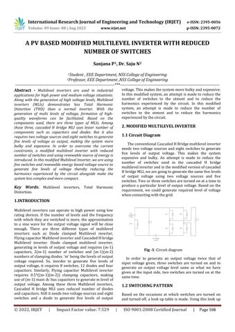
Multilevel inverters can operate in high power using low rating devices. If the number of levels and the frequency with which they are switched is more, the approximation to a sine wave for the output voltage signal will be close enough. There are three different types of multilevel inverters such as Diode clamped Multilevel inverter, FlyingcapacitorMultilevelinverterandCascadedHbridge Multilevel inverter. Diode clamped multilevel inverter, generating m levels of output voltage and requires (m-1) capacitors, 2(m-1) number of switches and (m-1)(m-2) numbersofclampingdiodes.‘m’beingthelevelsofoutput voltage required. So, inorder to generate five levels of output voltage, it requires 8 switches, 12 diodes and four capacitors. Similarly, Flying capacitor Multilevel inverter requires 0.5*((m-1)(m-2)) clamping capacitors, making useof(m-1)maindcbuscapacitorstogeneratemlevelof output voltage. Among these three Multilevel inverters, Cascaded H bridge MLI uses reduced number of diodes andcapacitors.Stillitneedstwovoltagesourcesandeight switches and a diode to generate five levels of output
voltage.Thismakesthesystemmorebulkyandexpensive. Inthismodifiedsystem,an attemptismadetoreducethe number of switches to the utmost and to reduce the harmonics experienced by the circuit. In this modified system, an attempt is made to reduce the number of switches to the utmost and to reduce the harmonics experiencedbythecircuit.
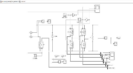
TheconventionalCascadedHBridgemultilevelinverter needs two voltage sources and eight switches to generate five levels of output voltage. This makes the system expensive and bulky. An attempt is made to reduce the number of switches used in the cascaded H bridge multilevelinverterandinthemodifiedversionofcascaded HbridgeMLI,wearegoingtogeneratethesamefivelevels of output voltage using two voltage sources and five switches.Twoorthreeswitchesareturnedonatatimeto produce a particular level of output voltage. Based on the requirement, we could generate required level of voltage whenconnectingwiththegrid.
In order to generate an output voltage twice that of input voltage given, three switches are turned on and to generate an output voltage level same as what we have given at the input side, two switches are turned on at the sametime.
Based on the occasions at which switches are turned on andturnedoff,a lookuptableismade.Usingthislookup
International Research Journal of Engineering and Technology (IRJET) e-ISSN: 2395-0056
tablewecouldeasilydeterminewhichswitchesareturned on and turned off at a particular time period and then it will be easy to develop a switching pattern. For instance, toget V1 voltageasoutput,S1 andS3 willbeturnedonand diode will beforwardbiased.Inthelookuptable,turning on of switches is represented in one's and turning off is represented in zeros. Since diode is a unidirectional device,itwillpreventbackflowofcurrentfromoccurring.
Sl:No Voltage level
S1 S2 S3 S4 S5 Diode
1 0 1 1 0 0 0 0
2 V1 1 0 1 0 0 1
3 V1+V2 1 0 1 0 1 0
4 V1 1 0 1 0 0 1
5 0 0 1 1 0 0 0
6 -V1 0 1 0 1 0 1
7 -(V1+V2) 0 1 0 1 1 0
8 -V1 0 1 0 1 0 1
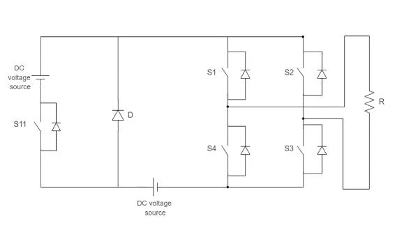
Fromthislookuptable,switchingpatternisdeveloped. If the total time period is T seconds, then from the lookup tablewecanobservethatswitchS1 isturnedonforhalfof the time period and the remaining time it is kept in off mode.
Herewearegivingaswitchingfrequencyof50Hz.So,the total time period will be around 0.02 seconds. And then we can say that switch S1 is turned on for half the time periodandthenturnedofffortheremaininghalf.Thatisit is turned on for 0.01 seconds and kept turned off the remaining period. Five levels of voltages, OV, +V, -V, +2V and -2V can be generated using this switching pattern usingonlyfivenumberofswitches.
Simulation is made using MATLAB/SIMULINK. Circuit diagram is made using blank model of MATLAB and using powergui, simulation is executed. By switching properly using pulse generator, output voltage levels can be generated.
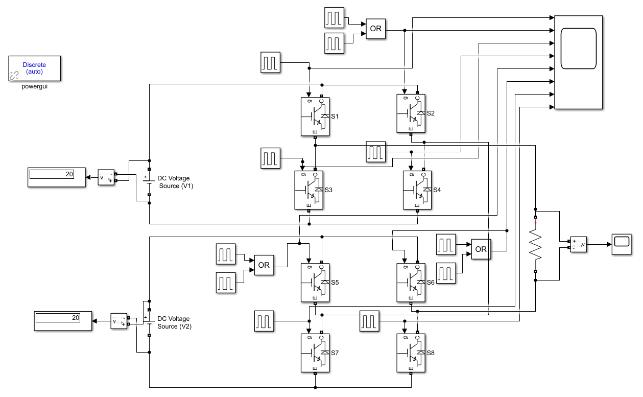
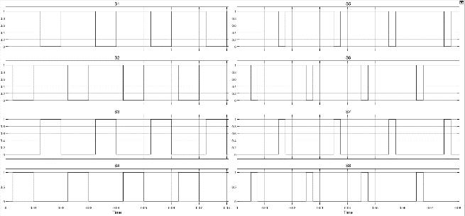
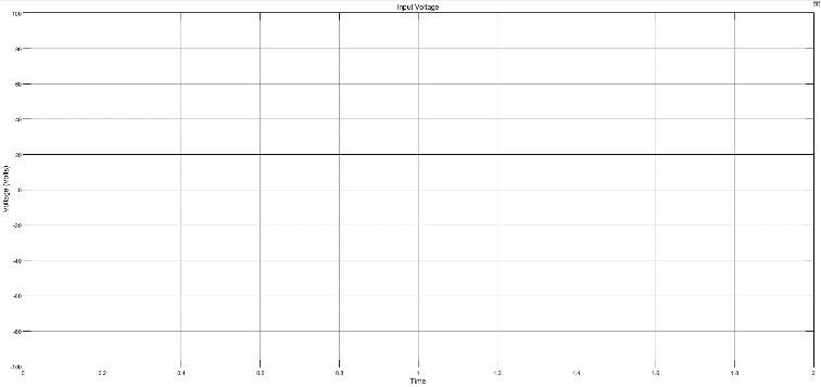
Inputvoltageof20Voltisgivenasvoltageattheinputside. Pulse generator is set with a switching frequency of 50Hz and corresponding switching is given. Output voltage waveform and gate pulses are observed. Input voltage waveformisasshowninFig3
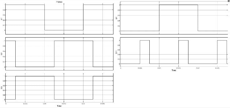
Thegatepulsesaregeneratedusingtheswitchinglook uptable,thegivenpulsesareevaluatedusingscope.Pulses givenforeachswitchesS1,S2,S3, S4, S1’,S2’,S3’,S4’.
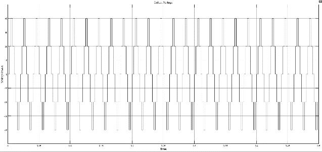
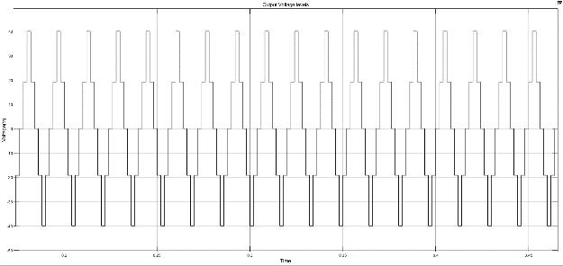
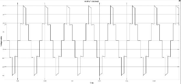
Withthegivenpulses,outputvoltageobtainedisasshown inFig4.Fivelevelsofoutputvoltagewithvoltagelevels0 Volt,20Voltsand40Voltsobtainedforaninputof20V fromDCvoltagesource.
ModifiedMultilevelinverterismadewithreducednumber ofswitchesandwithsamenumberofvoltagesourcesasin
Volume: 09 Issue: 08 | Aug 2022 www.irjet.net p-ISSN: 2395-0072 © 2022, IRJET | Impact Factor value: 7.529 | ISO 9001:2008 Certified Journal | Page 599
International Research Journal of Engineering and Technology (IRJET) e-ISSN: 2395-0056
Volume: 09 Issue: 08 | Aug 2022 www.irjet.net p-ISSN: 2395-0072
cascadedHbridgeMLI.Thefiveswitchesarearrangedina particular topology so that while turning on 2 or more switches,desiredvalueofoutputvoltagecanbegenerated.
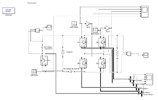
Simulation is done in MATLAB/SIMULINK. 20 V is given usingeachvoltagesourcesandgatepulsesaregivenusing repeating sequence block. Simulink model of modified MultilevelInverterisshowninFig5.
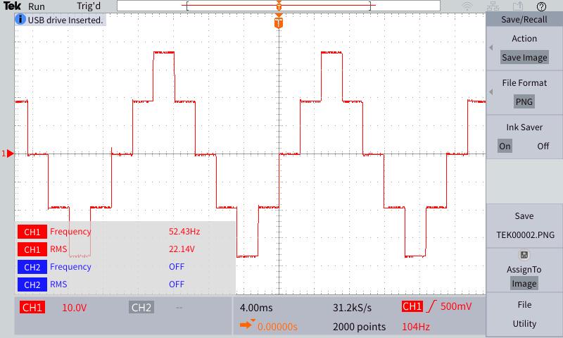
Fig -7:OutputVoltageofmodifiedMLI
Unwanteddistortionsinthepowersystemcreatesincrease in current in power system which results in high temperaturesinthecomponentsthatweareusing.So,itis crucial toanalyzeandmitigatetheharmonicsexperienced bythesystem.
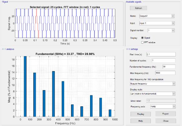
Fig -8:THDofCHBMLI
Fig -6
Input Voltage waveform, gate pulses given and output voltagewaveformisobserved.InputVoltagewaveformand GatepulsesgiventothefiveswitchesisasshowninFig 6. The output voltage waveform obtained after giving these gatepulsesisshowninFig7
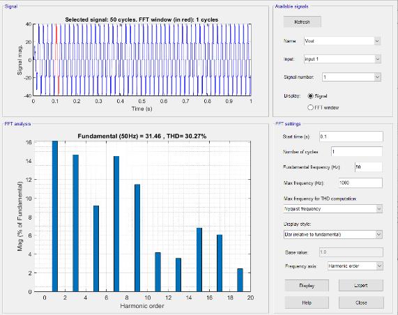
Fig -9:THDofModifiedMLI
Total Harmonic Distortion (THD) experienced by the CascadedHBridgeMultilevelinverterisshowninFig8
TheTHDobservedincascadedHbridgemultilevelinverter isaround30.27\%
TheTHDofmodifiedmultilevelinverterisaround28\%. Whichisless thantheconventional system.So wecansay
International Research Journal of Engineering and Technology (IRJET) e-ISSN: 2395-0056
Volume: 09 Issue: 08 | Aug 2022 www.irjet.net p-ISSN: 2395-0072
that, with the reduction of switches in the multilevel inverter,harmonicscaneasilybereducedtoacertainlevel.
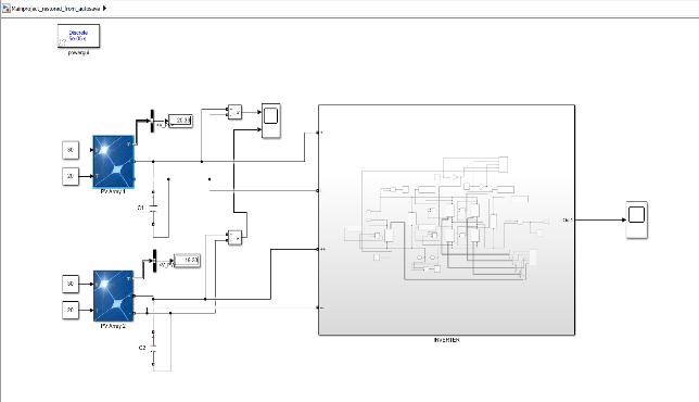
Multilevel inverters require more than one voltage sources for its proper working. Making use of DC voltage sources like batteries may make the system more bulky. By making use of renewable source of energy as the supply, its easy to give power to the system and thus it becomesmorecompact.
With the given gate pulses, output voltage waveform obtainedisasshowninFig12.
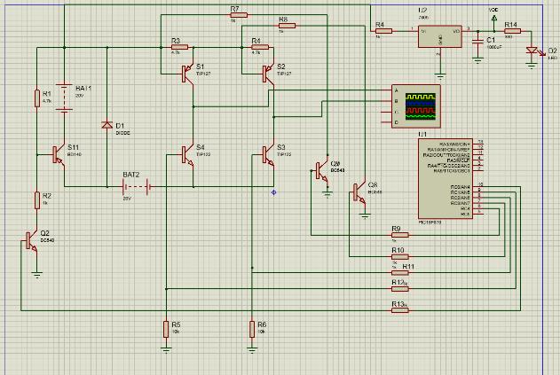
Proteus is a design software used for electronic design automation. It is used to create schematics and electronic prints and to generate PCB layout for printed circuit boards(PCBs).
Fig -10:PVbasedModifiedMLI
Programming language used is C programming using mickroC software. Switching pattern is fed within a while loopandthenpulsesaregenerated.
Fig -11:InverterSubsystem
PV array panel in MATLAB/SIMULINK is used as the voltage source for the simulation. Irradiance of 30 W/m2 and temperature of 200C is given as input to PV panel using constant block. PV panel is set with 36 cells using user defined option in PV array. If the voltage generated by each cell isaround 0.56 Volt, then the expected output voltage from the solar panel will be (0.56*36) = 20.16 Volts.FromFig10,theoutputfromsolarpanelisobserved to be around 20 Volt from one panel and 19 Volt from another panel. These two voltages are fed to the inverter subsystem shown in Fig 11. Simulation parameters is as showninlookuptable.
Irradiance 30W/m2 Temperature 200C
Cellspermodule(Ncell) 36 Resistor 100ohms
#include<xc.h> voidmain(void) { trisc=0; portc=0; delay_ms(500); while(1){ portc.f0=0; portc.f1=1; portc.f2=1; portc.f3=0; portc,f4=0; delay_us(2500); portc.f0=0; portc.f1=1; portc.f2=0; portc.f3=1; portc.f4=0; delay_us(2500);
International Research Journal of Engineering and Technology (IRJET) e-ISSN: 2395-0056
Volume: 09 Issue: 08 | Aug 2022 www.irjet.net p-ISSN: 2395-0072
portc.f0=1; portc.f1=1; portc.f2=0; portc.f3=1; portc.f4=0; delay_us(2500);
portc.f0=0; portc.f1=1; portc.f2=0; portc.f3=1; portc.f4=0; delay_us(2500); portc.f0=0; portc.f1=0; portc.f2=0; portc.f3=1; portc.f4=1; delay_us(2500); portc.f0=0; portc.f1=0; portc.f2=1; portc.f3=0; portc.f4=1; delay_us(2500); portc.f0=1; portc.f1=0; portc.f2=1; portc.f3=0; portc.f4=1; delay_us(2500); portc.f0=0; portc.f1=0; portc.f2=1; portc.f3=0; portc.f4=1; delay_us(2500);
Ports represented here refers various pins of the microcontroller. Portc.0 is 10th pin of microcontroller PIC16F676. Portc.1 represents 9th pin, portc.2 represents 8thpin,portc.3 represents 7thpinand portc.4represents 6thpinofmicrocontroller.
Microcontrollerpin10isusedforS11controlPins9,8,7,6 are for the control of switches S1, S2, S3, S4 respectively. Thus pulses are generated in each pin of the microcontrollertodriveeachswitches.
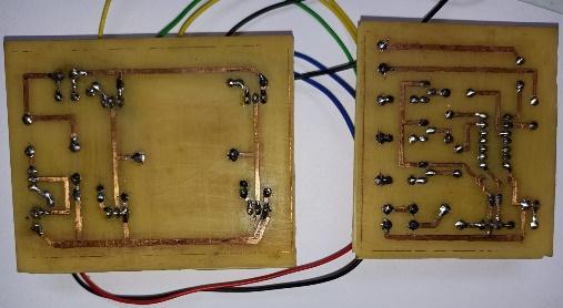
Connection using microcontroller is done using proteus softwaresothatitwillbeeasytogeneratethePCBlayout ofthewholesystem.Showninfigure13.
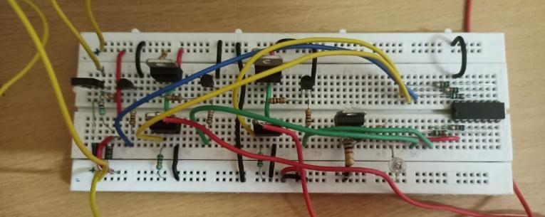
Breadboard connection of the whole circuit is made to checkthefeasibilityoftheconnectionasshowninFig14
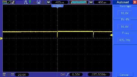
The output voltage obtained from the Digital Storage OscilloscopeisasshowninFig15
International Research Journal of Engineering and Technology (IRJET) e-ISSN: 2395-0056
Volume: 09 Issue: 08 | Aug 2022 www.irjet.net p-ISSN: 2395-0072
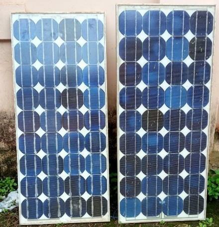
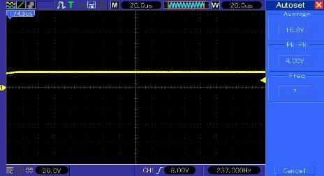
OutputfromthesolarpanelsisasshowninFig17.Thisis givenasinputtothecircuitconnection.
Fig -17:OutputfromPanel1
By keeping the DSO in measurement mode, Peak to peak voltage, mean value of voltage and frequency of the waveformiseasilyobtained. FromFig15, wecanseethat the output voltage obtained is around 79 Volts and frequencyisaround50Hz.
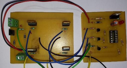
WiththeusageofPVpanel,DCvoltagesourcesthatmakes the system bulky, can be replaced. PV panel and etched circuitboardisasshowninFig16.
Peak to peak value of 16 volt and 7 volt is obtained from theoutputofsolarpanel.
Based on the input voltage waveform obtained, five level output voltage with a maximum peak to peak value of 56 Voltsandafrequencyaround50Hzcanbeobserved.
With the advancements in technology, development of cleanandmorecompactformofpowerelectronicdevices plays a pivotal role for the furtherance in aiding sustainableenergyscheme.Theroleofmultilevelinverter in that is unavoidable. Through this project aiming at reducing the number of components used in a conventionalmultilevelinverter,asmalladvancementcan be made in this arena. Initially, by comparing the structuresof modified MLIwiththeconventional oneand by evaluating the harmonics developed by both of them, we could conclude that the modified MLI demonstrates reducedharmonicsthanconventionalsystemandthereby we can speculate that the modified MLI is more advantageous and compact than conventional cascaded H bridgemultilevelinverter.
ThisprojectissupportedbyKSCSTE-SARDGovernmentof Kerala for the purchase of lab equipment. Also, thanks to allthefacultiesofElectricalandElectronicsDepartmentof NSS college of engineering, Palakkad for extending all the supportfortheimplementationoftheproject.
International Research Journal of Engineering and Technology (IRJET) e-ISSN: 2395-0056
Volume: 09 Issue: 08 | Aug 2022 www.irjet.net p-ISSN: 2395-0072
[1] Mittal, Arvind and Janardhan, Kavali and Ojha, Amit, "Multilevel inverter based Grid Connected Solar Photovoltaic System with Power Flow Control," 2021 International Conference on Sustainable Energy and FutureElectricTransportation(SEFET),2021.
[2] M. J. Uddin and M. S. Islam, "Implementation of CascadedMultilevelInverterwithReducedNumberof Components," 2021 2nd International Conference on Robotics, Electrical and Signal Processing Techniques (ICREST),2021
[3] H. Jafari, M. Hassanifar, D. Nazarpour and S. Golshannavaz, "Design and Analysis of a New Multilevel Inverter with Reduced Number of Switching Devices," 2021 12th Power Electronics, Drive Systems, and Technologies Conference (PEDSTC),2021.
[4] Y. Kumar, A. Saxena and M. Goyal, "Integration of Hybrid Cascaded Multilevel Inverter Configuration in a PV based Applications with Multicarrier PWM Technology," 2021 International Conference on Advances in Electrical, Computing, Communication andSustainableTechnologies(ICAECT),2021
2022, IRJET | Impact Factor value: 7.529 | ISO 9001:2008 Certified Journal | Page