International Research Journal of Engineering and Technology (IRJET) e-ISSN:2395-0056

Volume: 09 Issue: 08 | Aug 2022 www.irjet.net p-ISSN:2395-0072
International Research Journal of Engineering and Technology (IRJET) e-ISSN:2395-0056
Volume: 09 Issue: 08 | Aug 2022 www.irjet.net p-ISSN:2395-0072
 Kapil Budhathoki, Professor Dr. M. Asha Rani
Jawaharlal Nehru Technological University Hyderabad, India Department of Electronics and Communication Engineering, Jawaharlal Nehru Technological University Hyderabad, India ***
Abstract – The high-tech and most sophisticated facilities ever that we have been enjoying in our life have only been possible due to the conscientious research and development over a long span of time. The main focus of this project is in the design of a home automation system or a smart home providing new and exciting facility within. Based on the scheduling algorithm, status of our home is monitored through the use of various sensors. To increase the features, controlling of appliances through voice command has been incorporated. Thus this project adds flexibility addressing the potential problems faced by physically-challenged or handicapped type of people. [1]
Key Words: HomeAutomation,IoT,RoundRobin,ARM7, LPC2148,SpeechProcessing
Home automation or smart home has always been an interest for us. In such field also the technology is gradually becoming matured while providing high end security along with smart features. Providing real-time surveillance is a major concern for modern security systems.
Furthermorerapidlydevelopingtechnologydoesnotseem to fully confront the problems of physically-challenged or handicappedtypeofpeople.Thereportpreparedjointlyby theWorldHealthOrganizationandtheWorldBankinJune 2011 shows that about 15 percent of the world’s population, which accounts 785 million people, has significantphysicalormentaldisability.
Thusthisprojecthasaddressedsomeofthosecases.Bythe useofvoicerecognitionmoduledifferenthomeappliances are controlled. This helps such people to control home appliances according to their voice commands. Furthermore various sensors like PIR sensor, smoke sensorandtemperaturesensorareusedtodetectintruder, smoke and temperature. Alert messages are then sent to somepre-definedcellofthefamilymembers.[2]
This project makes use of ARM7 based LPC2148 microcontrollerandPICmicrocontrollertointerfaceallthe sensorsandvoicemodule.
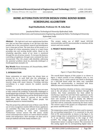
The overall block diagram of this project is as shown in figure 1 which consists of two intelligent units, i.e. two controllers. One is a main control unit which is developed on a LPC2148 board while the other unit, controlled through PIC microcontroller, is interfaced with three differentsensorstomonitorthestatusofhome.
During the hazardous situation at home, a text message is sent to the cell phone of family members through GSM modem. Also home automation has been added by interfacing a speech kit such that home appliances can be controlled according to the given voice commands. The main unit consists of GLCD to display the different parameters of home status. Here three sensors have been used that will be continually monitoring the home status. The sensors used in this project are temperature sensor, gassensorandPIRsensor.[7]
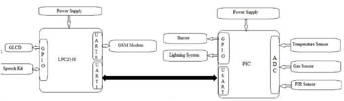
Thetemperaturesensor(LM35)hasbeenusedtomeasure the surrounding temperature. It is connected to the port PA.0 of PIC microcontroller as shown in the figure 2. Its outputvoltagevalueis proportional tothetemperature in 0C. It can measure temperature in the range of -550C to1500C. The voltage signal that is generated by the temperature sensor is analog in nature. The conversion of this analog signal into its corresponding digital value is
International Research Journal of Engineering and Technology (IRJET) e-ISSN:2395-0056
Volume: 09 Issue: 08 | Aug 2022 www.irjet.net p-ISSN:2395-0072
basedonsuccessiveapproximation method.Theanalog to digital conversion module is built in feature of PIC microcontroller.Eachanalogsampletakesabout2.44μsto convert into its corresponding digital value. The PIC16F877A microcontroller by default has 10-bit resolution,i.e.theconversionofananalogsignalresultsin corresponding10-bitdigitalnumber.[8]
5 SignalGroundCommonreferencevoltage
6 Data Set Ready (DSR) Incoming handshaking signal 7 Request To Send (RTS) Outgoing flow control signal 8 Clear To Send (CTS) Incoming flow control signal 9 RingIndicator(RI)(fromDCE)Incomingsignal fromamodem
Theresolutionisgivenbytheformula
ResolutionofADC=(+Vref–(-Vref))/(210-1) (2.1) whereVrefisreferencevoltage.
This gives the minimum voltage required to change the ADC result by one bit. Thus there are 1023 voltage steps between 0 volts and +5 volts. So each step is about 5000mV/1023 steps. Suppose the digital value of temperature sensor of 45 means 45*(5000/1023) = 220mV
Since10mV=10Cthusitcorrespondsto220C.Inthisway we can get the temperature value in degree centigrade scale.Afterconvertingtheanalogvoltagesignalintodigital form it is transmitted through the USART port of PIC microcontroller to the LPC2148 board for displaying the temperaturevalueinGLCD.Thedatatransmissionisdone throughRS232levelserialcable.Thepinconfigurationfor 9pinconnectoronaDTEdeviceisshownbelow.
1. Carrier Detect (CD) (from DCE) incoming signalfromamodem
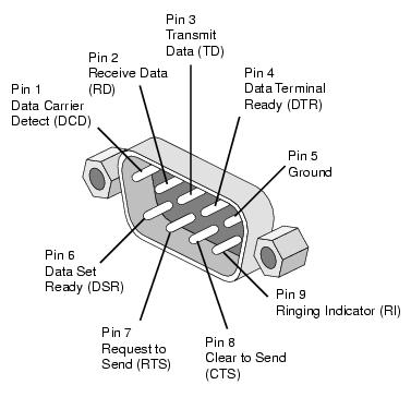
2 ReceivedData(RD)IncomingDatafromaDCE
3 TransmittedData(TD)OutgoingDatatoaDCE
4 Data Terminal Ready (DTR) Outgoing handshakingsignal
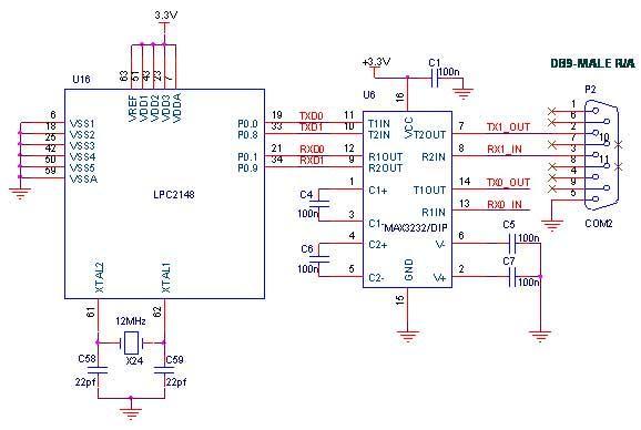
Hereweconnectonlysecond,thirdandfifthpinsforserial communication through UART ports between PIC and LPC2148 microcontrollers. Through TD wire data from a DTE device is transmitted to a DCE device. This wire is usedbyaDCEdevicetoreceiveitsdata.TheRDwireisthe one on which data is received by a DTE device. The connectionofUARTportofLPC2148microcontrollerwith DB9 is as shown in the figure 4. It is connected through MAX3232 which converts signals from RS-232 serial port tosignalssuitableforuseinTTLcompatiblelogic.Whena MAX3232ICreceivesaTTLleveltoconvert,itchangesTTL logic 0 to between +3 and +15 V, and changes TTL logic 1 tobetween-3to-15V,and viceversa forconvertingfrom RS232 to TTL. The configuration of the registers use for UART in LPC2148 and PIC microcontroller has been discussed in the later section. Once the digital data get transmitted to the LPC2148 microcontroller, it is converted into the corresponding temperature value in centigrade scale. Finally the temperature is displayed in
International Research Journal of Engineering and Technology (IRJET) e-ISSN:2395-0056
Volume: 09 Issue: 08 | Aug 2022 www.irjet.net p-ISSN:2395-0072
GLCD.TheGLCDcanbeconfiguredasdiscussedinthelater section.[3]
microcontroller.Inthiswayallthepossiblemeasureshave been applied to make people secure about the dangerous situationinhome.[10]
The next sensor that has been used is PIR sensor. It is connectedtotheportPA.2ofPICmicrocontroller.ThePIR sensor is used to detect the movement of intruder or anybodywhopassthroughbasedontheinfrared(IR)light emitted by the objects nearby. These sensors commonly use Fresnel lenses and have an effective range of ten meters. As all the objects having temperature above absolutezero,thelowerlimitoftemperatureat-273.150C, emit heat energy in the form infrared radiation which is invisible to human eye, these sensors can actually detects thechangeintheinfraredradiation.
The next sensor used is catalytic gas sensor. It has been connected to the port PA.1 of PIC microcontroller. It is usedtodetecttheleakageofgasinthehouse.Thereading ofthissensoristheoffsetvoltagegeneratedby thewheatstone bridge circuit. It is also analog in nature. Thus it is also converted into digital form based on the same successive approximation method as in temperature sensor. After analog to digital conversion completion, the digitized value is transmitted to LPC2148 microcontroller through the UART ports of PIC and LPC2148 in the same wayasexplainedearlier.Nowthisvalueiscomparedwith thepresetvaluetodeterminewhetherthereisgasleakage in the house or not. The preset value is adjusted by the potentiometerprovided.Ifthevalueobtainedfromsensor exceeds the preset value, an alert message is sent to the cellphoneofthefamilymemberthroughGMSmodem.The GMS modem is connected to the UART0 of LPC2148. The configuration of registers for UART in LPC2148 is discussed in the later section. The message is transmitted through GSM modem using AT commands. An example of GSMATcommandforsendingmessageisasshownbelow: [5]
Initially, when turned ON, the PIR sensor will adjust according to the environment. Then if there is any movement around the vicinity of the sensor, it can detect the change in intensity level of IR light. This IR radiation received is analog in nature. It is converted into digital form by the built in analog to digital conversion module whichisbasedonsuccessiveapproximationmethod.After conversionintodigitalform,thisdataistransferredtothe LPC2148 through UART ports of PIC and LPC2148. This serial transmission process has been explained earlier. Now this value is compared with the preset value to determine the intruder/human movement around the house. The preset value is set using the potentiometer provided. Thus it can be adjusted according to the environmental conditions. If the value obtained from sensor exceeds the preset value, an intruder message is displayed in the LCD and also the light bulb is turned ON. So that it provides more security during night time. The light bulb is connected through the relay connected to the portPB.1ofPICmicrocontroller [7]
Eachsensorwillmonitorthehomestatusinacyclicorder. Thesensorswillhavetheirtimeslicetomonitorthestatus or sense the physical environment. The sensors will be monitoring the home status in Round-robin fashion. Here equal time slices are assigned to each sensor in a circular order.
First the cell number to which message has to be transmitted is defined using AT command “CMGS”. After thatrequiredstring tobesentiswritten. Thus inthis way analertmessagecanbetransmitted.Furthermore,analert message is also displayed in the GLCD. As the leakage of gas is detected, buzzer is also turned ON to give notification about the dangerous situation at home. The buzzer is connected to the port PB.2 of PIC
Furthermore,homeautomationfeaturehasbeenextended using speech kit. We can control various home appliances usingthisspeechkit.Thespeechkithasbeenconnectedto the port P1.16 for turning ON the light and to port P1.17 forturningOFFthelight.Thespeechkitperformsinthree mainstepswhichareexplainedbelow.
Now research in speech processing has grown intense.Controllinghomeappliances, robots,toysthrough yourvoicecommandsseemstobethebestchoices.Inthis project also speech kit has been used to control the home
International Research Journal of Engineering and Technology (IRJET) e-ISSN:2395-0056
Volume: 09 Issue: 08 | Aug 2022 www.irjet.net p-ISSN:2395-0072
applianceslikelightbulb.Thelightbulbcanbe turnedON or OFF based on your voice commands. So it increases usability of the system as disabled or handicapped people canalsouseitatease.
The main unit of the speech kit is HM2007 speech recognition circuit. It also provides flexibility because it can be trained in any languages. For the speech kit to operate,itmustbefirsttrainedproperly.
Speechistypicallysampledatahighfrequency,e.g.16KHz overamicrophoneor8KHzoveratelephone.Thenweget adiscretesequenceofamplitudevaluesovertimedomain. A speech recognition system involves some steps as explainedbelow:
1.Convertingsoundintoelectricalsignals:Whenwespeak into microphone it converts sound waves into electrical signal. The electrical signal strength from the microphone varies in amplitude overtime and is referred to as an analoguesignalorananaloguewaveform.
2. Background noise removal: The ASR program removes allthenoiseandgetsthewordsthathavebeenspoken.
3. Breaking up words into phonemes: The words are broken down into individual sounds known as phonemes, whicharethesmallestsoundunitsnoticeable.
4. Matching and choosing character combination: this is themostcomplexphase.Theprogramhasbigdictionaryof popularwordsthatexistinthelanguage.EachPhonemeis matched against the sounds and converted into appropriate character group. This is where problem begins. It checks and compares words that are similar in sound with what they have heard. All these similar words arecollected.
5.Languageanalysis:hereitchecksifthelanguageallowsa particularsyllabletoappearafteranother.
6. After that, there will be grammar check. It tries to find outwhetherornotthecombinationofwordsanysense.
7. Finally the numerous words constitution the speech recognition programs come with their own word processor, some can work with other word processing packagelikeMSwordandwordperfect.
ThemainadvantageoftheICHM2007isthatitprovidesa completepackageforspeechdetectionpurpose.
During speech acquisition, speech samples are obtained from the microphone in real time and stored in memory for preprocessing. Speech acquisition requires a
microphone coupled with an analog-to-digital converter (ADC) that has the proper amplification to receive the voice signal, sample it, and convert it into digital speech. Thesystemsendstheanalogspeechthroughatransducer, amplifies it, and sends it through an ADC. The received samples are stored into memory on a RAM. We can easily implement speech acquisition with the HM2007 IC. The microphone input port with the audio codec receives the signal, amplifies it, and converts it into 8-bit PCM digital samples at a sampling rate of 3.57MHZ. The HM 2007 IC requiresinitialconfigurationortrainingofwords,whichis performed using a programming board. In the training process user trains this IC by speaking words into the microphoneandassigningaparticularvalueforthatword. Forexampleaworld“ON”canbeassignedavalue04or18. This can then be later connected to a microcontroller for furtherfunctions.
The speech signal consists of the uttered digit along with a pause period and background noise. Preprocessing reduces the amount of processing required inlaterstages.Generally,preprocessinginvolvestakingthe speechsamplesasinput,blockingthesamplesintoframes, and returning a unique pattern for each sample, as describedinthefollowingsteps.
1. The system must identify useful or significant samples fromthespeechsignal.Toaccomplishthisgoal,thesystem dividesthespeechsamplesintooverlappedframes.
2. The system checks the frames for voice activity using endpointdetectionandenergythresholdcalculations.
3.The speechsamplesare passedthrougha pre-emphasis filter.
An important part of speech recognition kit is training. Training involves creating a pattern representativeofthefeaturesofaclassusingoneormore testpatternsthatcorrespondtospeechsoundsofthesame class. The resulting pattern (generally called a reference pattern) is an example or template, derived from some type of averaging technique. It can also be a model that characterizesthereferencepatternstatistics.
The keypad and digital display are used to communicate with and program the HM2007 chip. The keypad is made up of 12 normally open momentary contact switches. Whenthecircuitisturnedon,“00”isonthedigitaldisplay, the red LED (READY) is lit and the circuit waits for a command.
International Research Journal of Engineering and Technology (IRJET) e-ISSN:2395-0056
Volume: 09 Issue: 08 | Aug 2022 www.irjet.net p-ISSN:2395-0072
During training every word is stored to a specific two digit number. So a particular word that has been storedcanbecleared.Afterawordnumberisentered,CLR function key pressed clears that particular word. All the saved words can be cleared at a time. For this enter 99 through keypad then CLR function key after RESTART. Duringtheclearingprocessredledwillblinkcontinuously.
To train the speech kit first any two digit number should be chosen except 00 and 99. After entering a two digit number, TRN function key is pressed and the required word is spoken. That word is saved to the corresponding wordnumber.
Ifmorethantwodigitsareenteredonlythelasttwodigits willbetakenintocount.
Forexample:
13 CLR clears the pattern corresponding to the word number13
25TRNtrainsthepatternforwordnumber25
2345TRNtrainsthepatternforwordnumber45
In this case, no voice input is accepted until WAIT pin is backto“H”state.
HereRDYissettolowandthespeechkitbecomesreadyto accept the voice input for recognizing. We must train the word patterns before beginning the recognition process. Afterthecompletionofrecognitionprocess,theresultwill appearintheD-buswiththeDENpinactive.
Thespeechkit,inthisproject,hasbeenusedtocontrolthe homeapplianceslikelightbulbinthiscase.Theturningof lightONhasbeenstoredtowordnumber07whileturning oflightOFF hasbeenstored towordnumber08. Theport P1.16 has been used to turn ON the light while port P1.17 isusedtoturnOFFthelight.[9]
Thegeneral16*2LCDshavetheirownlimitations that they can display only characters and numbers. In Graphical LCDs images can also be displayed. The
Graphical LCDs find applications in mobile screens, video gamesandotherdisplayunits.
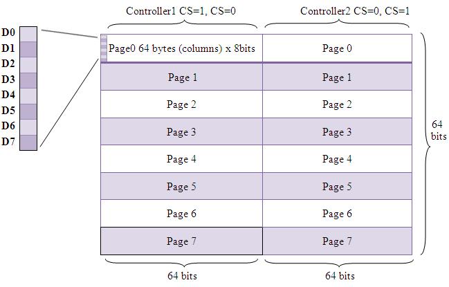
The GLCD used in my project is CFAG12864B which has a display format of 128*64 dots. The GLCD is divided into twoequalsectionsforinternaloperations.
Eachhalfiscontrolledbyacontroller.Thefigure5explains about the internal structure of 128*64 GLCD. From the figureabovewecanseethatthereare128columnsand64 rows making a total of 8192 pixels. Each half consists of eight pages. CS in the diagram above stands for controller (chip)select.Eachpageagainconsistsofeightrowsand64 columns. Thus two horizontal pages make 128 (64*2) columnsandeightverticalpagesmake64(8*8)rows.
Unlike,generalLCD,everydotinthepageshouldbetaken into considerations whether to set it high or low while displaying any character, symbol or image. To display thosecharacters,imagesorsymbolswehavetochoose an appropriatematrixsize.Thecharacterscanbedisplayedin thefollowingpattern:
A={127,9,9,127,0,0} B={127,73,73,54,00}andsoon.
International Research Journal of Engineering and Technology (IRJET) e-ISSN:2395-0056
Volume: 09 Issue: 08 | Aug 2022 www.irjet.net p-ISSN:2395-0072
register 6 Read data when High/Write data at High to Low transition (falling edge)
Enable(EN) 7 DataPin DB0 8 DataPin DB1 9 DataPin DB2 10 DataPin DB3 11 DataPin DB4 12 DataPin DB5 13 DataPin DB6 14 DataPin DB7 15 Chip selection for IC1; Activehigh CS1 16 Chip selection for IC2; Activehigh CS2 17 ResetSignal;Activelow RST 18 Output Voltage for LCD driving VOUT 19 BacklightVCC(5V) LED 20 BacklightGround(0V) LED
The CFAG12864B has 6 control bits which are used to control the operation and display data on the LCD. They arelistedbelowalongwiththeirportassignments.
Table3:Controlbitspinassignment PinNo. Symbol Function/Typical Value Port Assignment
the LCD – set high to read from the LCD to the MCU, set low to writefromtheMCUto theLCD
16 D/I Data/Instruction –tells the LCD whether ornot
data is being written to the screen or the MCU is using the data bits to perform an instruction – set high for data transfer and set low to designate and instruction is beingperformed
17 E Enable– The enableis used to clock operations to the LCD – it ends up being the clock of the LCD and when it clocks, sequential instructions are performed
C.4
C.5
The most commonly used and also confusing control bits are R/W, D/I, E. Enable must be set low and then high in order for an operation to be passed to the LCD. R/W and D/I are used to determine the mode of operation of the LCD. The following table will illustrate how these control bitsareusedtocontroloperations.
Table4:D/IandR/WmodesofOperation
D/I R/W Mode
12 CS1
Column/Chip Select 1Selects the left driver which is left half of screen
C.0 13 CS2 Column/Chip Select 2Selectstherightdriver which is right half of screen
0 0 An instruction is being written (such as defineYaddress)
0 1 MCU reads the status of the LCD – whether itisbusyorreadyforanothercommand
1 0 Data write – data is written to the display ramatwhateverX-Ycoordinateshavebeen set
15 R/W Read/Write – Selects the type of instruction being performed on
C.2
C.1 14 RST Reset – set high to reset the display, low otherwise
C.3
1 1 Data read – the data in the display RAM is readtotheMCU
International Research Journal of Engineering and Technology (IRJET) e-ISSN:2395-0056
Volume: 09 Issue: 08 | Aug 2022 www.irjet.net p-ISSN:2395-0072
Figure 6: Illustrating Left Half (or Right Half if CS2 = 1 and CS1 = 0)
There are about 8192 pixels on a 128*64 pixel GLCD screen and each pixel is controlled by a series of instructions. Figure 6 shows the left half of the screen (if CS1 is 1 and CS2 is 0). The Y address refers to which line the pixels should be written to and the X page sets the columntowhichtheywillbewrittento.
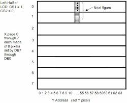
Therearebasicallythreestepsthatmustbedoneinorder to determine where the pixels will go. First the Y address must be set. The Y address actually has a counter so it needs only to be set once and then every time there is a datawriteitwillbeincrementedto thenextline.Secondly theXpageshouldbeset.Thisdetermineswhichcolumnof the screen will now be written to. Third, data write commandshouldbeissued.Everydatabitsmadehighwill bedarkenedontheYaddresslineintheXpage.Thedriver scans through the pages, using internal Y address counter to its advantage and resetting the X page (and eventually theCS)asitscansthroughthelines.
Anexampleofdisplayingawordisasshownbelow:
CHIP_SEL(TWO);//Selectingthesecondchipcontroller GLCD_CMD(0xBC);//SETXPAGETO4 GLCD_CMD(0x40);//SETYCOLTO0 GLCD_str("TEMP=");//WritingDataCommand
The process of selecting where on the screen the bit is going tobedisplayedisjust a narrowingprocess.CS1and CS2 narrow it down to half the screen. Y address narrows itdowntoa1bitwidestripeofheight64inthathalfofthe screen.Xpagepicksan8bitchunkofthis64bitstripeand
writedata writes 8 bits to that chunk. This is the way of puttingbitsonthescreen.
Here GLCD has been used to display the home status like temperature of the house. It also displays the alert message like “SMOKE DETECTED” and “PERSON DEECTED”.
ThevariousdatapinsofGLCDareconnectedtoportP0.16 to port P0.23 respectively of LPC2148 board. The other pins CS1, CS2, RS, RW, EN and RST are connected to port P1.18toportP1.23respectively.[11]
Globalsystemformobilecommunication(GSM) is a standard for mobile communication formed in 1982. A GSMmodemworksinawirelessradionetwork.HereGSM modem has been used to send text message to the family member‟s cell phone while there is any hazardous situationathome.ThisGSMmodemhasbeenconnectedto the UART0 of LPC2148 board. For the successful transmission of message UART port of LPC2148 must be configured.
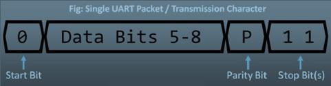
The LPC2148 contains two UARTs. In this project UART0 has been used for connecting the GSM modem. UART uses TxD (Transmit) Pin for transmitting data and RxD (Receive) Pin to receive data. UART sends & receives data in form of chunks or packets which are also referred to as „transmission characters‟. The structure of a UART datapacketisasshowninfigure7
LPC2148 has two UART blocks which are UART0 and UART1.ForUART0theTxDpinisP0.0andRxDpinisP0.1 andsimilarlyforUART1theTxDpinisP0.8andRxDpinis P0.9.BothUART0 andUART1blocksinternallyhavea 16byte FIFO (First in First Out) structure to hold the Tx and Rx data. Each byte in this FIFO represents a character which was sent or received in order. Both blocks also containtworegisterseach,fordataaccessandassembly.
The Tx has THR (Transmit Holding Register) and TSR (Transmit Shift Register). When we write data to be sent intoTHRitisthentransferredtoTSRwhichassemblesthe datatobetransmittedviaTxPin.
International Research Journal of Engineering and Technology (IRJET) e-ISSN:2395-0056
Volume: 09 Issue: 08 | Aug 2022 www.irjet.net p-ISSN:2395-0072
Similarly Rx has RSR (Receive Shift Register) and RBR (Receive BufferRegister). Whena validdata isreceivedat RxPinitisfirstassembledinRSRandthenpassedintoRx FIFOwhichcanbethenaccessedviaRBR.
We must first initialize and configure the UART block beforethosepinscanbeusedfordata transmission. Some of the registers used during data transferring are describedbelow.
U0THR(TransmitHoldingRegister):
It is an eight bit long register used to store the transmission of characters. We must set DLAB (Divisor LatchAccess)bitto0toaccessU0THRforwriteoperation.
U0RBR(ReceiveBufferRegister):
This is an eight bit long register used to store the serially receiveddata.ToproperlyreaddatafromU0RBR,wemust setDLAB=0,similartoU0THR.
U0DLLandU0DLM(DivisorLatchRegisters):
Both of these eight bit registers are combined together to form a 16-bit divisor value which is used to generate the baudrate.TheU0DLLholdsthelower8-bitswhileU0DLM holds the upper 8-bits making a total of 16 bits with the formation of “[U0DLM:U0DLL]”. As they form a divisor value, so the starting value for U0DLL is 0x01, since division by zero is invalid. Thus the starting value in combined formation is 0x0001. In order to access and use these registers properly, DLAB bit in U0LCR must be first setto1.
U0LCR(LineControlRegister):
It is an eight bit register which is used to configure the UARTblock(i.e.dataformatusedintransmission).
We should properly configure the Line Control Register whichisofthefollowingformat.
DLAB Break Control Parity Select Parity Enable Stop Bit Select Word Length Select
1. Word Length Select [Bit 0 and 1]: It is used to set the length of an individual data chunk. [00] represents the 5 bitdatalength.While[01],[10]and[11]represent6,7and 8bitdatalengthsrespectively.
2.StopBitSelect[Bit2]:Thisbitisusedtosetthenumber of stop bits to be used during the transmission of character. 0 is used for using 1 stop bit while 1 is used to representtheuseof2stopbits.
3. Parity Enable [Bit 3]: This bit is used to represent whether parity has been enabled or not. Making this bit 0 means parity generation and checking and has been disabledwhile1representsthatparityhasbeenenabled.
4.ParitySelect[Bit4and5]:Thesebitsrepresentthetype of parity that has been used. [00] represents the use of Odd-parity, [01] to represent the even parity, [10] to represent the forced 1 parity and [11] to represent the forced0parity.
5. Break Control [Bit 6]: This bit will set the break transmission.0isusedtodisablebreaktransmissionwhile 1isusedtoenableit.
6. Divisor Latch Access Bit [Bit 7]: This bit is used to set accesstothedivisorlatch.0isusedtodisableaccesstothe divisorlatchwhile1isusedtoenableit.Wecanaccessand configure the U0DLL and U0DLM registers only when it is enabled.GenerallywefirstsetDLABto1,configureDivisor LatchRegistersandagaindisableitbysetting0.
ByU0LCR=0x83; we can enable DLAB and configure those Divisor Latch registersandafterthatby U0LCR=0x03; wecandisableDLAB.
U0LSR(LineStatusRegister):
This8-bitlongregisterisusedtoknowthestatusofRxand Txblocks.Thisregisterisofthefollowingformat.
1.ReceiverDataReady(RDR)-[Bit0]:0meansthatU0RBR isemptywhile1meansU0RBRcontainsavaliddata.
2. Overrun Error (OE)-[Bit 1]: Overrun is the condition whenacharacterislostsincenodataiswrittenintoFIFOif it‟sfull.0meansOverrunhasnotoccurredwhile1means Overrunhasoccurred.
3.ParityError(PE)-[Bit2]:Whenthevalueoftheparitybit in the received character is in wrong state then a parity error occurs. 0 means parity error has not occurred while 1indicatestheoccurrenceofparityerror.
4. Framing Error (FE)-[Bit 3]: The framing error occurs when stop bit of a received character is zero. 0 means framing error has not occurred while 1 means framing errorhasbeenoccurred.
5. Break Interrupt (BI)-[Bit 4]: 0 means Break Interrupt hasnotoccurredwhile1meansithasoccurred.
International Research Journal of Engineering and Technology (IRJET) e-ISSN:2395-0056
Volume: 09 Issue: 08 | Aug 2022 www.irjet.net p-ISSN:2395-0072
6. Transmit Holding Register Empty (THRE)-[Bit 5]: 0 means U0THR contains valid data while 1 means it is empty.
7. Transmitter Empty (TEMT)-[Bit 6]: 0 means U0THR and/or U0RSR contains valid data while 1 means both U0THRandU0RSRareempty.
8.ErrorinRXFIFO(RXFE)-[Bit7]:0meansU0RBRhasno Rxerrorswhile1meansthatU0RBRhasatleastoneerror.
In the real world scenario there is a very rare chance to get the actual baud rates as desired. Most times the actual baud rate will drift a little about the desired value.Inshort,asmallamountoferrorinactualbaudrate isgenerallytolerableinmostsystems.
The main formula for calculating the baud rate is given as below:
BaudRate=PCLK in hertz/(16*(256*DLM+DLL)*(1+DIV ADDVAL/MULVAL))
wherePLCK=PeripheralClockinHertz
DLMandDLL=DivisorLatchregisters
DIDADDVALandMULVAL=Fractionalbaudrategenerator registers
The simplest method to calculate DLM and DLL is given below:
DLL=(PCLK/(16*Desired_BaudRate))%256
DLM=(PCLK/(16*Desired_BaudRate))/256
ThusforPCLK=30Mhzandforbaudrateof9600weget DLL=195and DLM=0
At first we must set DLAB to 1, thus the line control registerisinitiallyconfiguredas U0LCR=0x83; ThenwesetthevaluesforDLLandDLMasfollows U0DLM=0; U0DLL=195; InthenextstepweagainconfiguretheLCRdefiningother parametersasfollows U0LCR=0x03;
The data to be transmitted is first stored in THR. After every data transmitted, LSR is checked to know the completionofdatatransferasfollows
U0THR=data; while((U0LSR&0x40)==0);
Whenall thedata hasbeentransmittedthenthe7thbit in LSRwillbehighi.e.1.InsuchacasewhenitisANDedwith 0x40 the result will not be equal to 0. Thus the data transmission function will come out of the loop and stop transmission.Else,theANDedresultequals0andthedata transmissionprocesscontinuesanduntiltheend.
At the receiver end, the data received is stored in RBR. As the data is received, LSR is checked to know about the completionofdatareceptionasfollows while((U0LSR&0x01)==0); return(U0RBR);
When all the data reception has been completed, the first bit in the LSR will be high i.e. 1. In such a case, when it is ANDedwith0x01theresultwillnotbeequalto0.Thusthe data receptionfunction will comeout oftheloopandstop receivingthedata.Else,theANDedresultequals0andthe data reception process will continue until all the data has beenreceived.
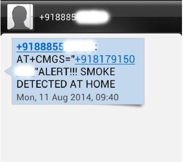
An example of GSM AT commands for sending message is asshownbelow:
UART0_SendStr("AT+CMGS=\"+918179150XXX\"\r"); delay(10);
UART0_SendStr ("ALERT!!! SMOKE DETECTED AT HOME");
First the cell number to which message has to be transmitted is initialized using AT commands. After that requiredstringissent.
MostoftheMicrochip‟sPICmicrocontrollershave built in USART Module. Here we will discuss about configuring the registers for data communication for PIC microcontrollers.
PIC16F877A USART PIC Microcontroller
TransmitStatusandControlRegister–TXSTA
Figure 8: Transmit Status and Control Register
2022, IRJET | Impact Factor value: 7.529 | ISO 9001:2008 Certified Journal | Page592
International Research Journal of Engineering and Technology (IRJET) e-ISSN:2395-0056
Volume: 09 Issue: 08 | Aug 2022 www.irjet.net p-ISSN:2395-0072
1. Clock Source Select Bit (CSRC)-[Bit 7]: This bit has no applicationinAsynchronousmodeoperationwhileusedto select master or slave mode in Synchronous mode operation.
2. 9-bit Transmit Enable Bit (TX9)-[Bit 6]: This bit when set enables the 9 bit transmission otherwise 8 bit transmission mode is used. The 9th bit is used as a parity bit.
3. Transmit Enable Bit (TXEN)-[Bit 5]: This bit when set enables the transmission. In the synchronous mode operationCERNandSRENbitsofRCSTAregisteroverrides thisbit.
4.USART mode select Bit (SYN)-[Bit4]: This bit isused to selectthemodeoftransmission.
1=Synchronousmode
0=Asynchronousmode
5.UnimplementedBit[Bit3]:Itisnotusedandreadas0.
6.HighBaudRateSelectBit(BRGH)-[Bit2]:Thisbitisused in Asynchronous mode operation and unused in Synchronous mode. Setting this bit enables High Speed whileclearingitenablesLowSpeedbaudrates.
7.TransmitShiftRegisterStatusBit(TRMT)-[Bit1]:Thisis TransmitShiftRegister(TSR)statusbit.Itisusedtocheck whether the data written to transmit register is transmittedornot.
1=TSRempty
0=TSRfull
8. 9th Bit of Transmit Data (TX9D)-[Bit 0]: This is the 9th bit of data in the 9 bit transmission mode. It is commonly usedasparitybit.
ReceiveStatusandControlRegister
1.SerialPortEnableBit(SPEN)-[Bit7]:Thisbitenablesthe serialport.
1 = Serial port enabled; configures RC7/RX/DT and RC6/TX/CKpinsasserialportpins
0=Serialportdisabled
2. 9-Bit Receive Enable bit (RX9)-[Bit 6]: Setting this bit enables 9 bit reception otherwise it will be in 8 bit receptionmode.
3.SingleReceiveEnableBit(SREN)-[Bit5]:Thisbithasno effect on Asynchronous mode and Synchronous Slave mode. Setting this bit enables Single Receive. This bit is clearedafterthereceptioniscomplete.
4. Continuous Receive Enable Bit (CREN)-[Bit 4]: Setting thisbitenablesContinuousReceive.InSynchronous mode CRENoverridesSREN.
5. Address Detect Enable Bit (ADDEN)-[Bit 3]: This bit is applicable only in Asynchronous 9 bit mode. Setting this bitenablesAddressDetect.
6. Framing Error Bit (FERR)-[Bit 2]: Detecting 1 at this position stands for Framing Error while 0 means No FramingError.
7. Overrun Error (OERR)-[Bit 1]: A high value at this positionindicatesthatOverrunErrorhasoccurred.
8. 9th Bit of received Data (RX9D)-[Bit 0]: This is the 9th bitofReceivedDataandiscommonlyusedasParityBit.
Baud Rate Generator provides the required clock for the data transmission and reception. USART module has a dedicated 8-bit baud rate generator that supports both Synchronous and Asynchronous modes. The 8-bit SPBRG registercontrolsthetimeperiodofthefreerunningtimer. Baud rate can be calculated from the following equations; whereFOSCistheclockfrequencyofthemicrocontroller.
International Research Journal of Engineering and Technology (IRJET) e-ISSN:2395-0056
Volume: 09 Issue: 08 | Aug 2022 www.irjet.net p-ISSN:2395-0072
3. GO/DONE: It gives the A/D Conversion Status. Setting this bit initializes A/D Conversion and will be automaticallyclearedwhentheconversioniscomplete.
4. ADON: This bit is used to switch ON/OFF the ADC module.Setting1turnsONwhile0turnsOFFthemodule.
1. ADFM: It is an ADC Result Format select bit. Two 8 bit registers(ADRESHandADRESL)areprovidedto storethe 10-bit result of A/D Conversion. When ADFM is 1, the result will be right justified, i.e. Most Significant Bits of ADRESHwillbereadas0.WhenADFMis0,theresultwill beleftjustified,i.e.LeastSignificantBitsofADRESLwillbe readaszero.
2. ADCS2: It is used to select A/D Conversion Clock in associationwithADCS1andADCS2ofADCON0register.
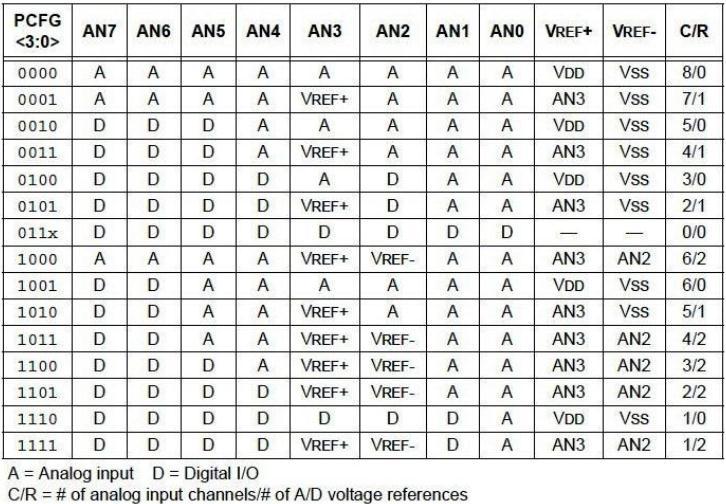
3. PCFG3-PCFG0: These are the A/D Port Configuration Control bits. Each pin among AN0 – AN7 is configured as analog,digitalorreferencevoltageinputsaccordingtothe statusoftheseconfigurationbitsasgivenbelow.
This sets the A/D Conversion Clock to Fosc/8 and also selects the Analog Channel 0. Finally the ADON set to 1 turnsONtheconvertermodule.
Now the format of storing the A/D result and A/D Port ConfigurationControlbitsissetasfollows: ADCON1=0x02;
This sets the A/D Result Format to left justified such that the Least Significant Bits of ADRESL will be read as zero. Nextthreeanaloginputchannelsareselected.
Now we configure the Transmit Status and Control Registerasfollows:
TXSTA=0x24;
This sets 8-bit asynchronous mode of transmission. Also transmit is enabled with High Baud rate. The Transmit Shift Register Status bit sets TSR full.The Receive Status andControlRegisterisconfiguredasfollows: RCSTA=0x90;
This configuration enables serial port and sets 8-bit reception. It also sets continuous reception. Here no framingerror,nooverrunerrorhavebeenset.[4]
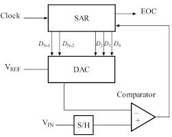
It is a technique used by the A/D conversion blocks for the process of analog to digital conversion in LPC2148 board. This technique performs binary search through all possible quantization levels before finally converging upon a digital output for each conversion. The successive approximation technique for analog to digital conversionhasfourmajorcomponents:
The sensors have been connected to the PORTA of PIC microcontroller.SothePORTAmustbeconfiguredasinput port.Thisisdoneasfollows:
TRISA=0xFF;
ThentheA/DConversionClockandanaloginputchannels areconfiguredas ADCON0=0x41;
International Research Journal of Engineering and Technology (IRJET) e-ISSN:2395-0056
Volume: 09 Issue: 08 | Aug 2022 www.irjet.net p-ISSN:2395-0072
1.Asampleandholdcircuittoholdtheinputvoltage,Vin
2. An analog voltage comparator that compares Vin with the output of the internal DAC and feeds the result of comparison to the successive approximation register (SAR).
3. A successive approximation circuit provides an appropriatedigitalcodeofVintotheinternalDAC.
4. A DAC supplies the comparator with an analog voltage equaltothedigitalcodeoutputoftheSAR. Initiallythesuccessiveapproximationregisterisinitialized in such a way that the most significant bit (MSB) is made equal to 1. Then this code is fed into the DAC which then generates the analog equivalent of this digital code. It is then compared with the sampled input voltage. If this analog voltage exceeds Vin, the comparator causes SAR to reset this bit otherwise the bit is left as 1. In the similar way,thenextbitissetto1andbinarysearchiscontinued until every bit in the SAR has been tested. The resulting code will be the digital approximate value of the sampled inputvoltageandisfinallyoutputbytheSARattheendof conversion(EOC).[6]
In this project all the objectives have been successfully achieved. We are able to control the home appliances through voice commands. The speech kit recognizes the given voice commands and controls the home appliances accordingly. The temperature is measured by a temperaturesensorLM35anditsvalueisdisplayedinthe GLCD.ThegassensorisusedtodetectthepresenceofLPG gas leakage or smoke with in the house. If it detects gas leakageorsmokewithinthehome,abuzzerwillturnONto notify the situation and also a text message is sent to the cell phone of family member. The GSM modem is used to send the text message. The GSM modem has been interfacedwiththeLPC2148board.
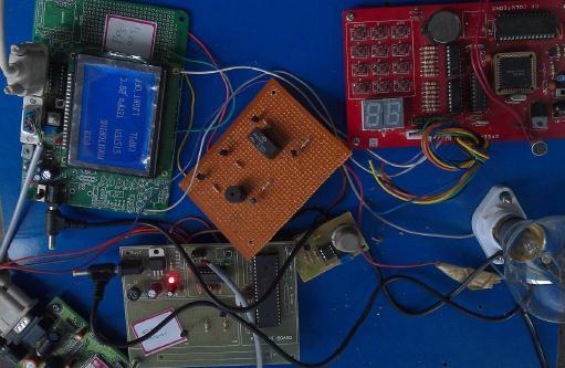
Thefigure14,asshownabove,demonstrates thelight OFF situation of my project. It was turned OFF accordingtothegivenvoicecommand.Allthemodules havealsobeenshownhere.Itisalsoshowingthevalue of temperature as “TEMP=280C” in the GLCD. The “LIGHTOFF”situationisalsodisplayedintheGLCD.
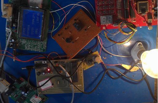
In the figure 15 we can see the light has been turned ON. It was turned ON by the voice command given throughspeechkit. Thelightbulbhasbeenconnected throughrelayasitneedshighervoltageleveli.e.220V.
The figure 16 shows the message that is received at the cell phone when some gas leakage or smoke is detected at home. As soon as the gas sensor detects hazardous situation at home, an alert message is immediately sent to the cell phone of family members throughGSMmodem.
International Research Journal of Engineering and Technology (IRJET) e-ISSN:2395-0056
Volume: 09 Issue: 08 | Aug 2022 www.irjet.net p-ISSN:2395-0072
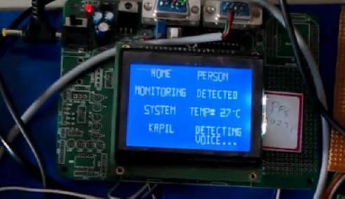
Inthe figure17wecansee that“PERSON DETECTED”has been displayed in the GLCD. As a PIR sensor detects some movementarounditsperipheral,itwillsensethechangein IR radiation. Then the message is displayed in the GLD aboutthesituation.
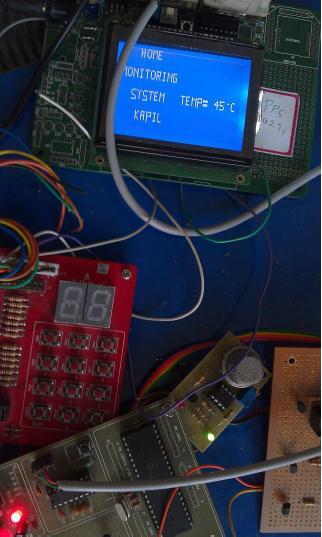
The figure 18 shows the led glowing when temperature reaches certain value. Here temperature limit has been adjusted to 450C. So as temperature reaches the preset valueledwillglowtoindicatethetemperatureexceed.
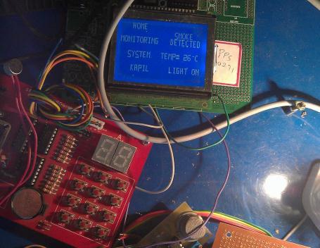
From the figure 19 as shown above, we can see the alert messagebeingdisplayedintheGLCDaftergasleakagewas detected by the sensor. The gas sensor was brought in contactwiththelighterthatcontainedbutanegas.
Figure 19: Figure to show when smoke detected
The speech kit used is not capable of recognizing long phrases. So it should be trained with short words only. Furthermore in the part of home automation only turning lightONandOFFhasbeentakenintoconsiderations.Other featuresforhomeautomationhavenotbeenincluded.The sensors have been used to monitor the home status in round-robinfashion.Othermethodscanbeimplemented.
In the case of future enhancement, high quality speech kit can be used so that it can recognize long phrases also. In case of providing home automation, some more features required in the home can be included. Also using RTOS othersuitableschedulingalgorithmscanbeincorporated.
Figure 18: Led glowing when temperature exceeds the limiting value
[1] Bo Cui and Tongze Xue, Design and Realization of an Intelligent Access Control System Based on Voice Recognition, 2009 ISECS International Colloquium on Computing,Communication,Control,andManagement [2] Rakesh V S, Sreesh P R and Sudhish N George, An Improved Real-Time Surveillance System for Home Security System using BeagleBoard SBC, Zigbee and FTPWebserver [3] Andrew N. SLOSS, Dominic SYMES and Chris WRIGHT “ARM System Developer‟s Guide Design and OptimizingSystemSoftware” [4]LPC214xUserManual,www.nxp.com/ [5]http://en.wikipedia.org/wiki/ARM7 [6]SuccessiveapproximationADC,
International Research Journal of Engineering and Technology (IRJET) e-ISSN:2395-0056
Volume: 09 Issue: 08 | Aug 2022 www.irjet.net p-ISSN:2395-0072
http://en.wikipedia.org/wiki/Successive_approximati on_ADC
[7]PassiveInfraredSensor, http://en.wikipedia.org/wiki/Passive_infrared_sensor
[8]LM35Precisiontemperaturemeasurementand calibration, http://www.magicsnotebook.com/lm35.html
[9]Speechrecognition, http://en.wikipedia.org/wiki/Speech_recognition
[10]ATCommandsInterfaceGuide,05thApril2002, WAVECOM
[11]LCD-128H064A, http://www.vishay.com/displays/list/product37329/