Studies On Switching Losses In Electric Vehicle Drive Train System
Rashmi S Hugar1, Dr S Vasudevamurthy21PG Student, Department of EEE, Dr. AIT, Bengaluru, Karnataka, India
2Associate Professor, Department of EEE, Dr. AIT, Bengaluru, Karnataka, India ***

Abstract The losses in a converter is an important aspect for the development of converters with performant features such as high reliability and efficiency, cost-effectiveness and high-power density. Power losses are generally controlled by modification of electric parameters in interleaved boost converter and cascaded H-bridge multilevel inverter. Batterypowered electric vehicle technology is gaining importance. In internal combustion engine vehicles power loss is more. EVs (Electric vehicle) use electric motor instead of an internal combustion engine. In order to reduce losses in EVs powertrain system is used. powertrain system comprises of interleaved boost converter and cascaded H bridge inverters. Interleaved boost converter is used to reduce the current stress and cascaded H-bridge multilevel inverter(MLI)isusedtoreducethevoltagestress.The analysis of power loss in each switch of interleaved boost converter and cascaded H-bridge multilevel inverter is investigated. The interleaved boost converter and cascaded H-bridge multilevel inverter model are developed, and simulated in MATLAB by usingSimulinksoftware.Simulationresultindicatethat a significant reduction loss is achieved by using interleaved boost converter and cascaded H-bridge multilevel inverter. A prototype model of hardware is implemented and the results are validated with simulation.
Keywords—Interleaved boost converter, cascaded H-Bridge MLI, power loss model.
1.INTRODUCTION
Battery-powered electric vehicle technology is becoming more significant in the modern era. Power electronic converters contain a significant amount of semiconductor components. Researchers are working to develop an effective and dependable powertrain system because the powertrain is responsible for transferring stored energy from the vehicle's battery system to the motors [1]. Power electronics inverters must operate distortion-free, electromagnetically compatible, have high-power factor and be extremely reliable while converting AC/DC. Compared to conventional silicon (Si) technology, wide band gap (WBG) semiconductor presently have higher-
levelmaterial properties and have better performance in high power EV applications [2]. Policymakers & stakeholders arecurrently working onadvance market share for electric cars. Power electronics experts are working to improve EV power electronic systems through increased power density and reducing cost to thesystem,size,andvolume.TheDC/ACinverteristhe essential section in EV, controls the battery power as well as drives the electric motor. The development of converters with excellent reliability and efficiency, low cost, and high-power density depend onthe losses of a converter. The modelling approach using software like LT spice or Saber is lengthy simulation period. By incorporating the small subintervals in the waveform duration of the inverter half bridge and also determining the transitional period for power dissipation, switching energies are estimated to use switchon,switchoff,aswellasriseandfalltimingsfor both Ids (MOSFET (drain-source) current) and Vds (MOSFET (drain-source) voltage) [5]. Datasheet charts canbeusedtodeterminetheelectrothermalproperties of MOSFETs. In this paper, an inverter model is proposedwhichrepresentstheoperationalbehaviorof a real inverter. The proposed system involving interleaved boost converter and h-bridge inverter, which is subsequently translated to a multi level inverterenablespreandpost-analysisofthesystemby modifying the operational switching frequency, circuit characteristics, and control architecture. Furthermore, the losses are measured and compared with conventional system. A prototype hardware model is implementedandverifiedwiththeresults.
International Research Journal of Engineering and Technology (IRJET) e-ISSN: 2395-0056
Volume: 09 Issue: 08 | Aug 2022 www.irjet.net p-ISSN: 2395-0072
2.SYSTEM DESCRIPTION
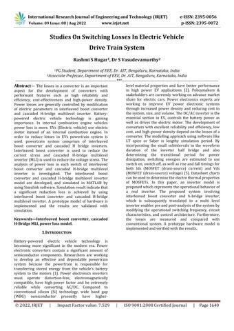
Theblockdiagramfortheproposedsystemisprovided inFig1:
Fig 1 : Proposedsystemconfiguration
Inthis,thedcvoltagesourceisprovidedforinterleaved boost converter in which the source voltage is getting boosted and provided to H-Bridges individually in the five level Cascaded H-Bridge Multi Level Inverter (CHBMLI) connected to R load. The losses are less in theabovementionedsystemcomparedtoconventional system as the current stress in dc-dc converter switch is reduced due to interleaving of the converters and voltagestressacross theinverterswitchesarereduced as it deals with only half the system voltage. Total power losses of the inverter, based on conduction loss andswitchingloss,areprovidedbelow:
IftheMOSFETisnotconducting:
Fig 2:Powerlossmodelofinverter
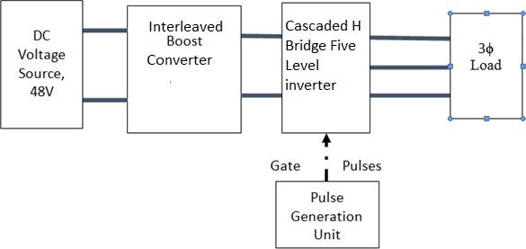
Theconductionlossofthehalf-twobridge'sswitchesis determined by internal on-state resistance and transientcurrent,asshowninequationbelow:
Thetotalpowerlossesofconductionaredescribedas:
The conduction loss of the half-two bridge's diodes is determined by the internal resistance of the diode, the voltage drop across the diode, and the transient current,asshowninequation below
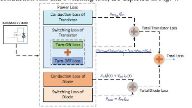
The power loss equations during switching of the halfbridgearegivenas:
Fs is the switching frequency. From all of the above equations of the switching loss, the total power losses ofswitchingaredescribedinequation:
3.INTERLEAVED BOOST CONVERTER
Thecircuitof interleavedboostconverterisprovidedin Fig3
Volume: 09 Issue: 08 | Aug 2022 www.irjet.net p-ISSN: 2395-0072
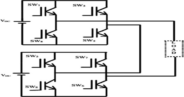
4. FIVE LEVEL CHBMLI INVERTER
Multilevel Inverters (MLI) are popular and available in hundreds of thousand inverters areavailable worldwide. Multilevel inverter have several benefits as well as capabilities. Cascaded H Bridge inverter is one of them (CHB). Overall, the CHB multilevel inverter's advantage is on improving output signalperformanceandeliminationofhigherpossibility of power device failure The specified single phase 5levelCHBMLIisshowninFig4.
Fig 3: Circuitconfigurationofinterleavedboost converter
WhenthedeviceS1isswitchedon,thecurrentflowing through the inductor iL1 grows linearly. During this time, power is stored within the inductor L1. When S1 is switched off, diode D1 conducts and the energy stored in inductor slopes down with such a slope determined by the difference in input and output voltage. The inductor starts to discharge and the currentistransferredtoloadviadiodes.S2isturnedon after half a switching period of S1, completing a same cycle of operations. Because the output capacitor combines both power channels, the effective ripple frequency is double that of a single-phase boost converter. The input current ripple has a small amplitude.
The following equations are used to design the boost converter circuit parameters The boost converterswitchgatesignaldutyratiois:
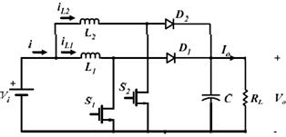
The following equation provides the inductor of a boostconverter: Theinductorripplecurrentis:
Theoutputcapacitanceoftheboostconverteris:
The output capacitor ripple voltage is determined byusing
Fig 4:FivelevelCHBMLI
Multilevel inverters have been created as a means of overcoming drawbacksof conventional inverters. They have some impressive features, including the ability to generate output voltage and current withleastamount of distortion and ability to operate at low switching frequencies.
Asaresultofmultiplyingitsinputvoltagesource(Vdc), the single phase 5-level CHBMLI produce five steps of output, including 2Vdc, Vdc, 0, -Vdc, and -2Vdc. The resulting AC output voltage swing across zero level from +2Vdc to -2Vdc. The function of Multilevel inverters are determined by the switch-close and switch-open states of each semiconductor device. The inverter's output value is determined by the switching state configurations. There are five possible configurations for the switching state in the five-level CHBMLI. Each configuration output voltage can be explainedas:
a) Mode 1:
InthisoperationtheS1,S2,S5,S6,areclosed,hencethe outputvoltageis2timeofVdc
International Research Journal of Engineering and Technology (IRJET) e-ISSN: 2395-0056
Volume: 09 Issue: 08 | Aug 2022 www.irjet.net p-ISSN: 2395-0072
Fig 5:Mode1equivalentcircuitof5levelCHBMLI
b) Mode 2:
InthisoperationtheS1, S2,S6,S8,areclosed,hence theoutputvoltageisVdc.
Fig 8:Mode4equivalentcircuitof5levelCHBMLI
e) Mode 5:
InthisoperationwhenS3S4,S7S8,areclosed,hence theoutputvoltageis2timeof–Vdc(negativepolarity).
Fig 6:Mode2equivalentcircuitof5levelCHBMLI
c) Mode 3:
In this operation the S2 S4, S6 S8 are closed, hencetheoutputvoltageis0volt
Fig 9:Mode5equivalentcircuitof5levelCHBMLI
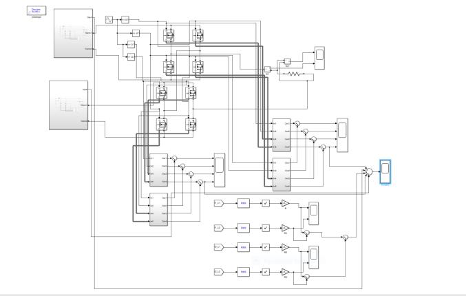
5. SIMULATION & HARDWARE RESULTS
The simulation circuit for the conventional single phaseinverterisprovidedinFig10:
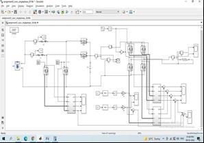
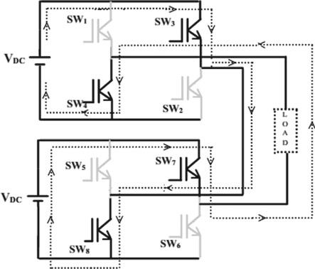
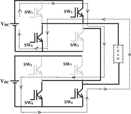
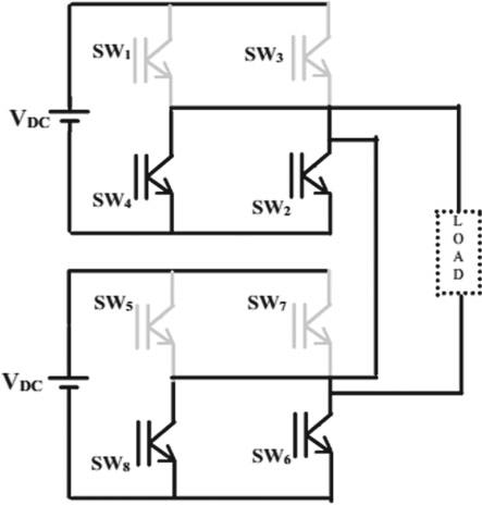
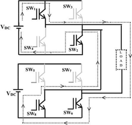
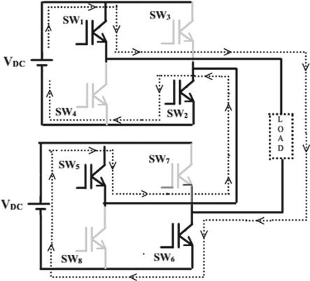
Fig 7:Mode3equivalentcircuitof5levelCHBMLI
d) Mode 4:
In this operation when S3 S4, S6 S8, are closed, hence theoutputvoltageis–Vdc(negativepolarity)
Fig 10:Simulationcircuitofconventionalsystem
International Research Journal of Engineering and Technology (IRJET) e-ISSN: 2395-0056
Volume: 09 Issue: 08 | Aug 2022 www.irjet.net p-ISSN: 2395-0072
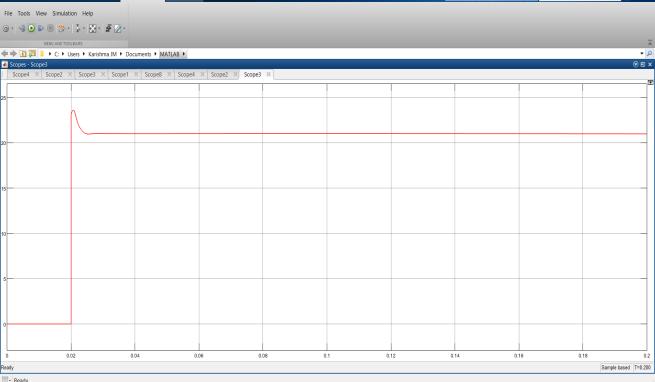
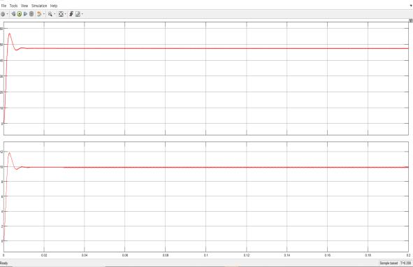
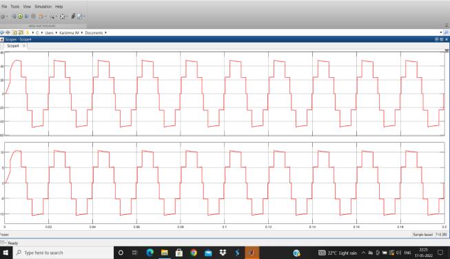
The single phase H-Bridge inverter in this system uses a battery with 12V DC voltage source that is increased to 48V by an interleaved boost converter. At eachstage,thelossesarecalculatedandtotallossesare computed Fig11representinterleavedboostconverter outputvoltageandcurrent:
Fig 13:Invertervoltageandcurrent
The output voltage is around 48V and current is around 10A. The inverter switch losses are provided below:
Fig 11:Interleavedboostconvertervoltageandcurrent
The output voltage is 48V and current is 11A. The Interleavedboostconverterswitchlossesareprovidedin Fig12:
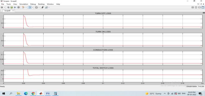
Fig 12:SwitchinglossesofInterleavedboostconverter
The boost converter total switching loss is 0.65W. The invertervoltageandcurrentisshowninFig13.
Fig 14:Theinverterswitchlosses
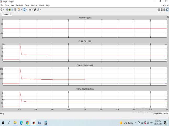
Thetotalswitchlossforinverterisaround19.5W.The overall switching losses including inductor core loss are providedinFig15:
Fig 15: Switchinglossesofconventionalsystem
The total losses are around 21W. The simulation circuit for the conventional three phase inverter is providedinFig16:
International Research Journal of Engineering and Technology (IRJET) e-ISSN: 2395-0056
Volume: 09 Issue: 08 | Aug 2022 www.irjet.net p-ISSN: 2395-0072
Theboostconvertertotalswitchlossis0.875W. Fig19providetheinvertervoltageandcurrent:
Fig 16: Simulationcircuitofconventionalthreephase system
12V DC is boosted to 48V by the interleaved boost converterandprovidedtothethreephaseinverter.The lossesarecalculatedateachstageandsumofthelosses arecomputed
Fig 17 show the output voltage and current of the interleavedboostconverter:
Fig 19: Inverterloadvoltageandcurrentofthreephase system
Theoutputvoltageisaround30Vandcurrentisaround 11A.TheinverterswitchlossesareprovidedinFig20:
Fig 17:Interleavedboostconverteroutputvoltageand current
Output voltage is around 48V and current is around 11A. The boostconverter switchlosses are provided in Fig18.
Fig 20: InverterSwitchinglosses
Thetotalswitch loss for inverter is around20.1W. The overall switching losses including inductor core loss in Fig21:
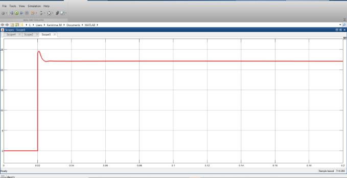
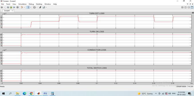
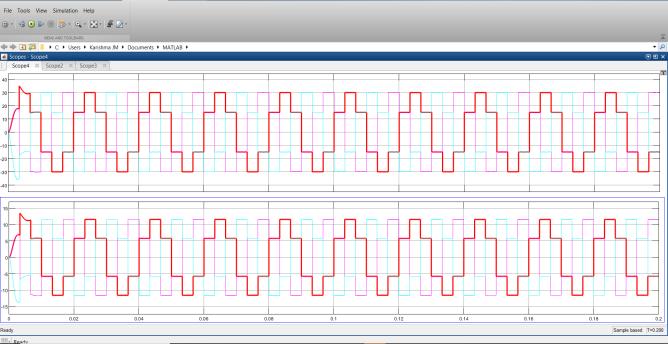
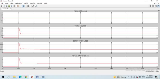
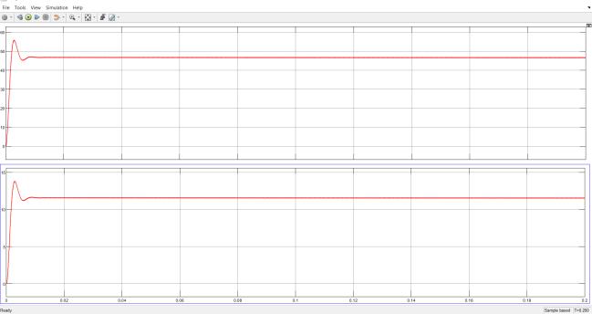
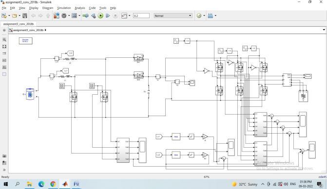
Fig 18: SwitchinglossesofInterleavedboostconverter
Fig 21: Overallswitchinglossesincludinginductor coreloss
The total losses are 22.1W. The simulation circuit for the proposed single phase 5 level CHBMLI isprovided inFig22:
International Research Journal of Engineering and Technology (IRJET) e-ISSN: 2395-0056
Volume: 09 Issue: 08 | Aug 2022 www.irjet.net p-ISSN: 2395-0072
Theboostconverterswitchinglossis0.1W.
TheinvertervoltageandcurrentisshowninFig25.
Fig 22: Simulationcircuitofproposedsystem
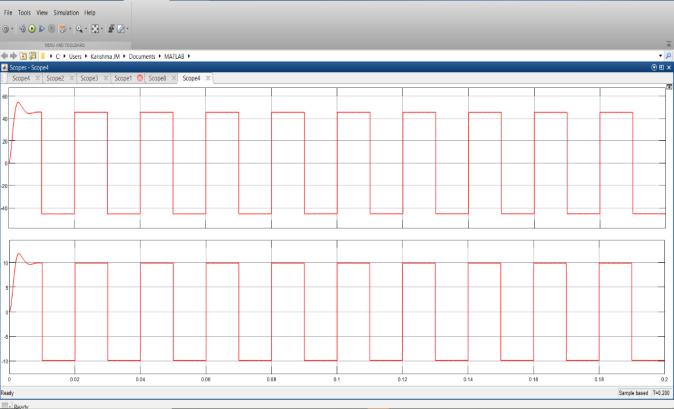
The battery of 12V is provided as source and it is boostedto24Vbytheinterleavedboostconverterand providedtoH-BridgeandoutputvoltageofcascadedHBridge inverter is 48V. The losses are calculated at eachstageandthesumofthelossesarecomputed.Fig 23 show the output voltage and current of interleaved boost converter
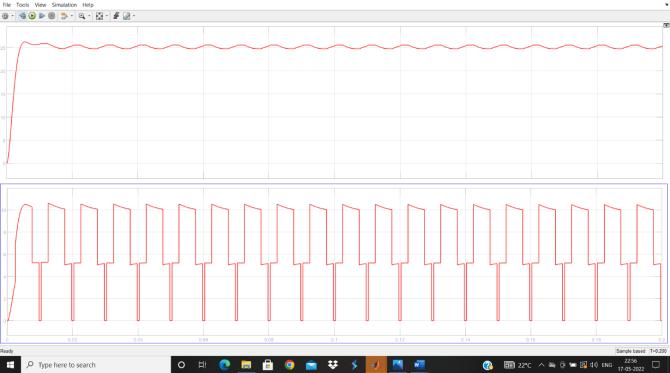
Fig 25:Inverterloadvoltageandcurrent
The inverter output voltage is 48V and current is 10A. TheH-BridgeswitchinglossesareshowninFig26.
Fig 23: Interleavedboostconvertervoltageandcurrent
Theoutputvoltageisaround25Vandcurrentisaround 11A. The interleaved boost converter switching losses areprovidedFig24:
Fig 26 :Switchinglossesof5levelinverter
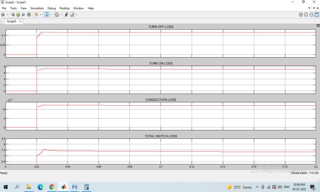
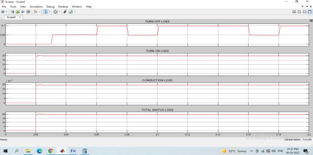
The total switch loss for inverter is 7.5W. Fig 27 represent the overall switching losses including inductor core loss
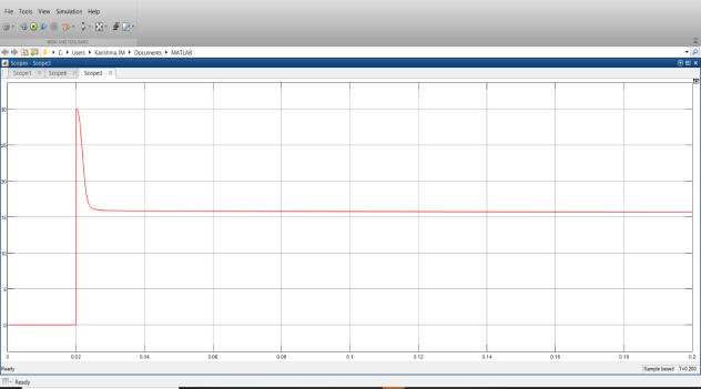
Fig 27: overallswitchinglossesofproposedsystem
Fig 24: SwitchinglossesofInterleavedboostconverter
Thetotallossesare15.75W.
6. Hardware Implementation
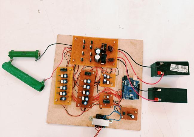
AsinglephaseACsupplyof230V,50Hzissteppeddown to12Vandconvertedto12VDCusingadioderectifier The rectified dc voltage is provided to 5V and 12V Voltage regulator. 5 V supply Arduino micro controller which generates the pulses according to the control strategy.12Vto drivercircuittodrivePowerElectronic switchesoftheproposedinverter.Itcanbedesignedby connecting two single phase bridge converters in cascade on load side. The interleaved boost converter boost DC voltage from 12 V to 24 V to s supply two HBridge converters. The load voltage is around 48 V. Fig 28showthehardwareimplementation.
The load voltage of the five level inverter is shown in Fig29:
Fig 28 :Hardwarecircuitofproposedsystem
A 230 V / 12 V, 0.75A stepdown transformer supply the switching circuit, controller, Pulse width modulation (PWM), signal generator and driver circuits. Rectified voltage is supplied to Arduino and driver IC TLP 250 and 5V regulator from which the bufferIC.
Arduino Atmega328 generate 50 Hz square wave, controlallthesignals,andprovidethegatesignaltothe MOSFET drivers that drive the switches. PWM IC TL494 is used for providing pulses to boost operation. The generated pulses are provided to buffer IC which isolates the driver circuit components and the controller. The output of buffer IC and the driver IC triggertheswitchesaccordingtopulses.
Fig 29 :5levelInvertervoltage
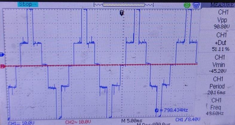
Thefirstlevelisaround24Vandsecondlevelisaround 24Vwhichprovidesthepeakacloadvoltageas48V.We getthefivelevelsas+48V,+24V,0,-24Vand-48V.
7. CONCLUSION
A power conversion system with boost converterand inverter is designed for providing power to single phase and three phase loads of 500 W from battery source. In order to reduce the current stress across the boost converter switch, the interleaving concept is used and the power losses were measured. Further by use of cascaded structureinverter topology, the voltage stress across the inverter switches are reduced and corresponding power losses were measured. The total power loss for conventional single phase inverter system is 21W and conventional three phaseinverterlossesis22.1W.Thelosseswithcascaded structure of multilevel inverter is 15.75W. The percentage of reduction of losses is around 25.1%. The simulation for the proposed system is carried out for a powerratingof500W.
A power conversion system with boost converterandinverterisdesignedandimplementedfor providingpower of 150 W to single phase . Due tocost considerations, a prototype hardware is implemented fortheproposedsystem.Intheimplementedhardware system,thepowerlossis14W.
REFERENCES
NO.8,P.1569,2019.
International Research Journal of Engineering and Technology (IRJET) e-ISSN: 2395-0056
Volume: 09 Issue: 08 | Aug 2022 www.irjet.net p-ISSN: 2395-0072
[2]. J. Reimers, L. Dorn-Gomba, C. Mak, and A. Emadi, “Automotive traction inverters: Current status and future trends,” IEEE Trans. Veh. Technol., vol. 68, no. 4, pp.3337–3350,2019.
[3]. Z. Zhou, M. S. Kanniche, S. G. Butcup, and P. Igic, “High-speed electro-thermal simulation model of inverter power modules for hybrid vehicles,” IET Electr. Power Appl.,vol.5, no. 8,pp.636–643, 2011.
[4]. B. N. Torsæter, “Evaluation of Switching Characteristics, Switching Losses and Snubber Design foraFullSiCHalf-BridgePower Module.”NTNU, 2016.
[5]. B. Agrawal, M. Preindl, B. Bilgin, and A. Emadi, “Estimatingswitchinglosses forSiCMOSFETswithnonflatmillerplateauregion,” in 2017 IEEE Applied Power Electronics Conference and Exposition (APEC), 2017, pp. 2664–2670.
[6]H.Rasool,A.Rasool,A.A.Ikram,U.Rasool,M.Jamil, and H. Rasool, “Compatibility of objective functions with simplex algorithm for controller tuning of HVDC system,” Ing. e Investing.,vol.39,no.3,2019.