International Research Journal of Engineering and Technology (IRJET) e ISSN: 2395 0056

Volume: 09 Issue: 07 | July 2022 www.irjet.net p ISSN: 2395 0072
International Research Journal of Engineering and Technology (IRJET) e ISSN: 2395 0056
Volume: 09 Issue: 07 | July 2022 www.irjet.net p ISSN: 2395 0072
Abstract primarily, testing printed circuit boards was manualandbasedontheboardstructure,wasalsolimited by the chip complexity. Also, it requires expensive testers andfixtures[1]
Theperformanceoftestersdependsbasicallyonthedevice properties. To enhance tester performance, the efforts should be focused on improving testing speed through decreasingtheinterconnectionsbetweenthetesterandthe deviceundertest[2].Thecomplexityoftheinterconnections betweenthedeviceundertest(DUT)andthetesterbecame oneofthemajorshowstoppersinevaluatingthehealthof DUT[3].Tosurpasstheseconstraints,weintroduceanew test methodology based on star test topology (STT) for connectingmultipledevices.Suchtopologyprovidesameans ofarbitrarilyobservingtestresultsandsourceteststimulus. The model requires minimal on chip/board resources (pins/nets). Also, it is not limited by the chip function or complexity.Thenewmethodologyinvolvesdevelopingone sharedtestaccessport(TAP)overtheentirePCBandare designoftheon chipDFTcircuitry.
Keywords Start test topology, STT, integrated circuit testing, bidirectional data line, higher functionality, test accessport.
The traditional testing methods is based on the board structure,alsoitslimitedbysuperfinechippackages,double sidedboards,conformalcoating,multi chipmodules(MCMs), andchipcomplexity.Also,itrequiresexpensivetestersand fixtures.Insuchtests,chipfunctionscanbeignoredforshorts testingandmustbeconsideredforcontinuitytests[5]
Theperformanceoftestersdependsbasicallyonthedevice properties.Toenhancetesterperformance,theeffortsshould befocusedonimprovingtestingspeedthroughdecreasing theinterconnectionsbetweenthetesterandthedeviceunder test.ThecomplexityoftheinterconnectionsbetweentheDUT and the tester became one of the major showstoppers in evaluatingthehealthofDUT[6].
Embedding memory and microcontroller units inside the testers also causes many disadvantages. It increases cost, size, and complexity of the tester. On the other hand, decreasingmemorysizeleadstoaproportionaldecreasein thenumberofdevicesthatcanbediagnosedbythetester. Versatileandmulti facetedtesterscanbemanufactured,but
***
the cost will be more expensive. The rapid growth in the complexityofcircuits
requires a parallel and continuous development in tester microcontrollers,creatingadifficultchallenge[7]
To surpass these constraints, we introduce a new test methodologybasedonJTAGandIEEE1149.1Std.Thenew methodologyinvolvesdevelopingonesharedtestaccessport (TAP)overtheentirePCBandare designoftheon chipDFT circuitry. Such improvements will lead to a significant reduction in the complexity of testing nets, resources, and pinsconnections[8].
Thenewmethodologyusesstartesttopologyforconnecting multiple devices; such topology provides a means of arbitrarily observing test results and source test stimulus. The model requires minimal on chip/board resources (pins/nets). Also, it is not limited by the chip function or complexity [9]. Moreover, test access is not limited by the physicalfactorsoftheboardandthetestgenerationishighly automated.
Inthenewmethodology,onlyonebidirectionaldatalineis utilized in order to carry data between the TAP and each deviceundertest.Therefore,onetestaccesspinisrequired for each DUT. The new architecture will definitely help in reducinganyresultantyieldlossduetotheprovencontact problems[10,11]
Manyfeaturesandadvantagesareachievedbyusingthenew methodology. One such feature is the considerable cost reductionduetoutilizingonlyoneTAPtointerfaceall on board devices, and also due to the high simplification in boundaryscancircuits.FurtheradvantageisthateachDUTis diagnosed separately without any correlation with other DUTs.Moreover,unliketheIEEE1149.1Std,thereisnoneed toembedinstructions,identifications,orbypassunitsinside integratedcircuits[12].
Aspreviouslymentioned,thenewmethodologyusesSTTto connect all the peripherals. Each DUT is connected to the central test access port TAP using point to point connections. The TAP acts as a hub and the DUTs are consideredasclients.Theconnectiondoesnotnecessarily have to resemble a star in order to be classified as a star topology,butalloftheDUTsaccesspinsmustbeconnected to one shared TAP. All traffic that traverses the testing
International Research Journal of Engineering and Technology (IRJET) e ISSN: 2395 0056
Volume: 09 Issue: 07 | July 2022 www.irjet.net p ISSN: 2395 0072
networkhastopassthroughthisTAP.Itselectsthetargeted DUT to be tested. It also forwards the test pattern and returnsthecorrespondingtestdataoutput(TDO)pattern. ToselectadifferentDUT,thecomputertransmitsatestreset signal (TRST) followed by a new data packet. The star topologyisaneasiertopologytodesignandimplement.
The most important advantage of STT is that it responds immediately to any node failure. Only one DUT will be affectedifanerroroccurs,whiletheentirecircuitremains running. Because ofthis, diagnosinga singledevice for an errorordefectissupposedtobeeasy.
In STT, the computer broadcasts test data input (TDI) packets to several DUTs via TAP, and the computer can easily identify any failed DUT. Because of its simplicity in testability, managing the STT using connected DUTs is consideredatriviallysimple Moreover,bySTT,failurescan belocatedeasilybyalogicalanalysisand,asaresult,itcan besimplydiagnosed.
ThenewsystemarchitectureisillustratedinFigure1;ithas TAPactingasmainhubandtheDUTsrepresentthenodes. Each DUT exploits only one pin to interface the TAP. Therefore,testsignalsaredirectlytransferredfromTAPto theDUTwithoutpassingthroughotherdevices.Toprevent driveconflictsamongtheDUTs,theTAPcontrollerhandlesa directaddressingmethod.
When a data packet is received by the TAP input line, the portreadstheaddressinformationinthepacketheaderto determine its ultimate destination. Then, using serial to parallel shift registers and de multiplexer circuits, it forwards the test packet to the next DUT on its journey; therefore,TAPperformsthe"datatrafficcontrol"functionon thecircuit.
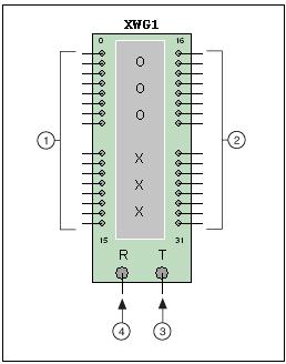
Each DUT has its own test hub TH. It is the circuit that interfacesmultipleinputsandoutputsoftheDUTandmakes themactasasinglenetworksegment.Theserialsignalthat isintroducedattheinputoftheTHappearsattheparallel outputsoftheTH.Itisspecializedhardwarethatforwards datapacketsbetweenTAPandDUTinputsandviceversa.
The circuit is designed and simulated before starting hardwarebuilding.WeusedtheNationalInstruments(NI) Multisim simulation and circuit design software version 12.0.1. It is sophisticated software that gives advanced designandanalysisfeaturesinordertooptimizeefficiency, shorten time and reduce design errors toward prototype. IntuitiveMultisimtoolsresultinsaved(PCB)iterationsand significantsavingsindesigncosts.
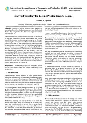
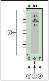
In order to simulate transmitting test patterns by the computer,weusedthe“WordGenerator”instrumentthatis available in the software. It can send digital words (bit patterns)intodigitalcircuits.Theinstrumentisdepictedin Figure1.
The output pins (1) which appear on the left side of the instrumentarethelastsixteenbitsinthe32 bitword,while theoutputpins(2)ontherightsideof theinstrumentare thefirstsixteenbitsinthe32 bitword.Label“T”refersto theexternaltrigger(T)terminal3,label“R”isassignedfor thedata readyterminal(4).
International Research Journal of Engineering and Technology (IRJET) e ISSN: 2395 0056
Volume: 09 Issue: 07 | July 2022 www.irjet.net p ISSN: 2395 0072
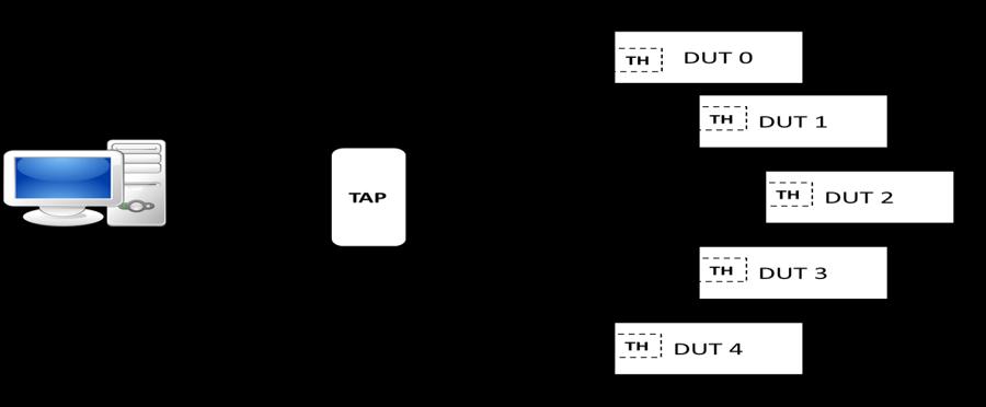
The word generator settings can be entered by double clickingontheinstrumentface.Figure1showsthesettings screenforthewordgeneratorinstrument.Asseenclearlyin thefigure,theoutputterminals(1)correspondtothoseon the icon. The buffer (2) generates pre defined patterns or savesdigitalpatterns.
resetsignalisgeneratedbythecounterunittostoprunning theloadingcontrolunit.
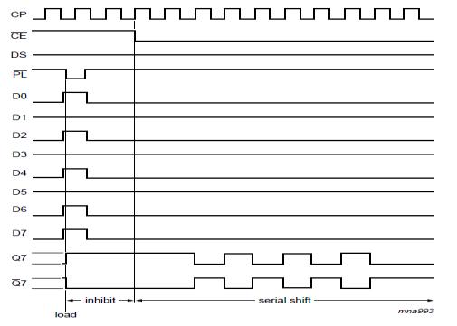
The circuit output signals are captured using the Logic Analyzerinstrument.Itcandisplayupto16digitalsignalsin acircuit.Thisinstrumentoffersanimprovedtiminganalysis and rapid data acquisition of logic states to help perform troubleshooting and design very large systems. Figure 3 showsthe icon ofthelogic analyzerinstrument.Section1 indicatestheinputterminals,section2istheexternalclock terminal,section3istheclockqualifierterminal,andsection 4isthetriggerqualifierterminal.
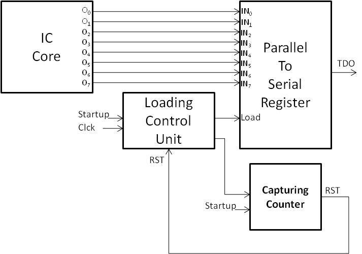
The circuit diagram shown in Figure 4 represents a TDO transmitterforafour outputIC.Theloadingcontrolunitis formedofaDflipflop(74HC74D).Itpossessesthreeinputs: startup,clock,andreset.Atthemomentthestartupsignal turnstohigh,theDflipflop generatesa loadsignal tothe shift register and the counter starts running. When the counterfinishescounting,itsendsaresetsignaltotheDflip flopcausingunloadfortheshiftregister.
The TDO transmitter circuit carries out capturing the responsesignalsoftheICundertestandbroadcastingitina serialmanner.Itincludesthreemainunits:loadingcontrol unit, parallel to serial shift register, and counter unit, as illustratedinFigure.ThestartupsignalgeneratedbytheTDI driver unit returns to play an important role in activating this unit; it stimulates the loading control unit to load the shiftregisterandalsoitswitchesonthecapturingcounter circuit.Thecapturingperiodisdeterminedbythecapturing counterrunningtime.Attheendofthecountingperiod,a
Since we utilize only one IN/OUT pin for testing, the TDO shouldbeshiftedoutserially,bitbybit.Forthisreasonwe usedaNXP 74HC165Nshiftregistertoperformparallelto serial shifting.The74HC165isa high speedSi gateCMOS devicethatcomplieswithjointelectrondeviceengineering
2022, IRJET | Impact Factor value: 7.529 | ISO 9001:2008 Certified
International Research Journal of Engineering and Technology (IRJET) e ISSN: 2395 0056
Volume: 09 Issue: 07 | July 2022 www.irjet.net p ISSN: 2395 0072
council(JEDEC)standard7A.Itispin compatiblewithalow powerSchottkyTTL(LSTTL).
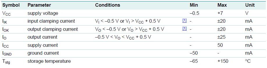
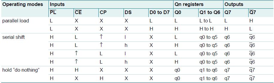
The 74HC165 are 8 bit, parallel load registers with complementaryserialoutputs.Theparallelinputdata(D0 D7) will be loaded asynchronously into the register if the parallelload( )inputis0.Otherwise,datapenetratesthe registerseriallybitbybitatthedateserial(DS)inputand shiftoncetotheright(Q0Q1Q2,etc.)witheachrising edgeclockpulseifandonlyifthe( )inputis1.Hence,by tying the DS input to the Q7 output we allow parallel to serialconverterexpansionofthesucceedingstage.Oneinput is allowed to be used as an active LOW clock enable (CE) input since the clock input is a gated OR structure. The assignmentfortheinputpinsCPandCEisarbitrary;itcan be rearranged based on the layout convenience. For predictableoperation,therisingedge(LOWHigh)ofthe inputCEcanonlytakeplacewhileCPisHigh.Toavoidany data shifting while is activated, either theca or the CE signals must be High before the rising edge of signal.Table4illustratesthefunctionaldescriptionforthe serialoutshiftregister.
Theproposedtestingcircuitwassimulatedsuccessfullyby NIMultisimsoftware.Itsmoothlytransmittedtestpatterns and received the corresponding response patterns. The circuit succeeded in testing four ICs accurately. Also, the hardware was built and ran successfully. It performed a precisetestingforseveralICs.
TheICresponsepatternmustbesettledontheshiftregister inputs for N clock pulses where N is the number of IC outputs.Thepatternwillbeloadedwhilethe inputislow. Whenthestartupsignalturnstohigh,the inputreceives aHighsignalfromtheDflipflopandtheshiftregisterstarts serializingthepattern(Figure 4 7).
Thisregisterischosenalsobecauseofitscapabilitytodeal withexcesscurrentsthatmayresultfromdefectiveICs.As listedinTable2,theregistercanaffordaninputclamping current of up to 20 mA. Moreover, it can be embedded in high temperature industrial integrated circuits with a temperatureupto150oC.
ThedrivingArduinosourcecodewaswritten,compiled,and loadedsuccessfully.Itpromptstheusertoentertheinitial values and accordingly drives the TAP interface. All the systempartssuccessfullyintegratedtogethertoperforman advancedandsophisticatedtest.
[1] C.A.Miller,"Contactlessinterfacingoftestsignalswitha deviceundertest",ed:GooglePatents,2011.
[2] M.H.Tehranipour,N.Ahmed,andM.Nourani,"Testing SoC interconnects for signal integrity using extended JTAGarchitecture", Computer AidedDesignofIntegrated Circuits and Systems, IEEE Transactions on, vol.23,pp. 800 811,2004.
[3] N.Ahmed,M.Tehranipour,andM.Nourani,"Extending JTAG for testing signal integrity in SoCs", in Design, Automation and Test in Europe Conference and Exhibition, 2003,2003,pp.218 223.
International Research Journal of Engineering and Technology (IRJET) e ISSN: 2395 0056
Volume: 09 Issue: 07 | July 2022 www.irjet.net p ISSN: 2395 0072
[4] B.Vermeulen,T.Waayers,andS.Bakker,"IEEE1149.1 compliantaccessarchitectureformultiplecoredebug on digital system chips", in Test Conference, 2002. Proceedings. International,2002,pp.55 63.
[5] L.Meng,Y.Savaria,Q.Bing,andJ.Taillefer,"IEEE1149.1 baseddefectandfaulttolerantscanchainforwaferscale integration", in Defect and Fault Tolerance in VLSI Systems, 2003. Proceedings. 18th IEEE International Symposium on,2003,pp.18 25.
[6] V.D.Agrawal,"Testingforfaults,lookingfordefects",in TestWorkshop(LATW), 201112thLatinAmerican,2011, pp.1 1.
[7] I.M.FilanovskyandB.Moore,"Contactlesstestingofon chip oscillator operation", in Circuits and Systems (ISCAS), 2012 IEEE International Symposium on, 2012, pp.2605 2608.
[8] M. Scandiuzzo, S. Cani, L. Perugini, S. Spolzino, R. Canegallo,L.Perilli, et al.,"Input/OutputPadforDirect Contact and Contactless Testing", in European Test Symposium (ETS), 2011 16th IEEE,2011,pp.135 140.
[9] E.J.Marinissen,D.Y.Lee,J.P.Hayes,C.Sellathamby,B. Moore,S.Slupsky, et al.,"Contactlesstesting:Possibility orpipe dream?",in Design, Automation&TestinEurope Conference & Exhibition, 2009. DATE'09.,2009,pp.676 681.
[10] G.P.AcharyaandM.A.Rani,"Surveyofteststrategies for System on Chip and it's embedded memories", in Intelligent Computational Systems (RAICS), 2013 IEEE Recent Advances in,2013,pp.199 204.
[11] M. Moganti, F. Ercal, C. H. Dagli, and S. Tsunekawa, "Automatic PCB Inspection Algorithms: A Survey", Computer Vision and Image Understanding, vol.63,pp. 287 313,1996.
[12] M.MogantiandF.Ercal,"ASubpatternLevelInspection SystemforPrintedCircuitBoards", ComputerVisionand Image Understanding, vol.70,pp.51 62,1998.
2022, IRJET | Impact Factor value: 7.529 | ISO 9001:2008 Certified Journal