Impact of Gate Length Modulation On a Al0.83Ga0.17N/GaN Dual Double Gate MOSHEMT for Radio Frequency Application
1PG Scholar, Department of Electronics and Instrumentation Engineering, Odisha University Of Technology and Research (OUTR), (Formerly College of Engineering and Technology), Bhubaneswar, Odisha, India
2Assistant Professor, Department of Electronics and Instrumentation Engineering, Odisha University Of Technology and Research (OUTR), (Formerly College of Engineering and Technology), Bhubaneswar, Odisha, India

3Professor, Department of Electronics and Instrumentation Engineering, Odisha University Of Technology and Research (OUTR), (Formerly College of Engineering and Technology), Bhubaneswar, Odisha, India ***
Abstract This work come across the capable strength of comparison of AlGaN/GaN under lap DG MOS HEMT and Dual DG MOS HEMT with variation of different gate length and has been investigated in Visual TCAD simulation. The device channel is a wideband mesh matched channel. of Al0.83Ga0.17N and slender band Gallium Nitride sheet, along with SiO2, Al2O3 and high K HfO2 as the dielectric of gate The key device performance parameters of analog and RF analysis is completed for a variety of different gate length (Lg). In scaling down of gate length (Lg) then increment in the drain current (ID), cut off frequency (fT), trans conductance (gm) happen and reduced in intrinsic gain (Av) and trans conductance generation factor(gm/ID) with respect to 1nm oxide thicknesses. The use of the double 2 DEG hetero structure helps to obtain outstanding device linearity and it also give the higher current according to gate length and from this simulation work we have revealed that the Dual Double Gate MOS HEMT's drain current is very high than DG MOS HEMT drain current i.e. 66.67%, and also found the peak cutoff frequency of approx 1766 GHz in DDG MOSHEMT. These results denote the capability of Al0.83Ga0.17N/GaN based Dual Double Gate MOSHEMT can be acceptable replacement for high current and high frequency performance
Key Words: DG MOS HEMT, DDG MOS HEMT, Gate Length, AlGaN/GaN 2 DEG hetero structure, TGF, Intrinsicgain, Cutofffrequency
1. INTRODUCTION
High electron mobility transistors based on AlGaN/GaN arethebesttransistorforhighfrequencyimplementation (HEMTs)[1] Because of the different band gap energies, an AlxGa1 xN/GaN hetero structure is produced when the AlGaN barrier is formed on a reasonably thick layer of GaN. [2 6]. In the upper region of the GaN layer, close to the boundary, the band bends, and electrons form a two dimensional conductive channel [7,8]. The 2 dimensional electrongas(2DEG)[9]features,whichariseattheAlxGa1 xN/GaNhetero structurewithouttheneedforanydoping
and are used to increase the frequency execution of AlGaN/GaN HEMTs, govern the execution of AlGaN/GaN HEMTs[10].By adding holes from the [p type] AlGaN to thehetero structure ofAlGaN andGaN,the2DEGdensity is raised. This can lead to conductivity modulation.AlxGa1−xNwithAlformationofabout0.83and GaN formation of about 0.17, and high quality AlxGa1 xN/GaN hetero structure[11]been fill out by the process ofmetalorganicchemicalvapordeposition(MOCVD).
Double Gate MOSFET structure has single material[12] that revealed increased exemption to short channel effects, but Double Gate MOS HEMT hetero structure[13 17]hasIII Vhetero structurelayerintothechannel offer high drain current. HEMTs are used inSoCsand it also known for low noise amplifiers and high drain current applications.HEMTtransistorsareuniqueanditisableto operate at very higher frequency than ordinary transistors, in low power amplifiers, satellite receivers, mobile phones, voltage converters, radar equipment, as well as in the defense sector. It is also employed in high frequencygoodslikethese.
As far as we are aware, 2 DEG's RF performance of AlGaN/GaN hetero structure based Dual Double Gate MOS HEMT device with variation of gate length has not been demonstrated yet. So we investigated the parameterssuchasID,gm,TGF(gm/ID),intrinsicgain(Av) and fT and comparable to the specifications of DG MOS HEMTanditsrangeofgatelengths(Lg).
2. DEVICE STRUCTURE
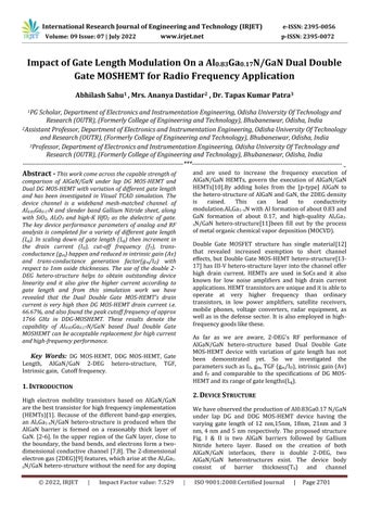
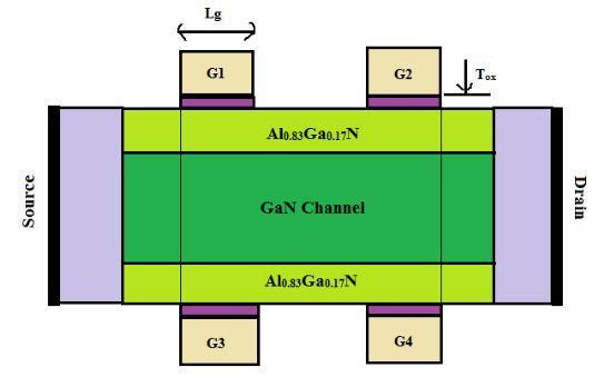
WehaveobservedtheproductionofAl0.83Ga0.17N/GaN under lap DG and DDG MOS HEMT device having the varying gate length of 12 nm,15nm, 18nm, 21nm and 3 nm, 4 nm and 5 nm respectively. The proposed structure Fig. I & II is two AlGaN barriers followed by Gallium Nitride hetero layer. Based on the creation of both AlGaN/GaN interfaces, there is double 2 DEG, two AlGaN/GaN heterostructures exist. The device body consist of barrier thickness(Tb) and channel
thickness(Tch)withupperandlowerbarrierthickness(Tb) of3nmandchannelthicknessof10nm,whereTsi = TCh + 2.Tb The conduction band edge of the AlGaN layer is offset with respect to the channel, and reducing traps at the interface through mesh matching with the GaN layer. Thelengthsofthesourceanddrainarefixed.Lun=5nm, and the high K HfO2 dielectric material's are of 1nm for both upper and lower gate oxide thicknesses (Tox). Both the structure consist of gate with different length i.e in DG MOS HEMT there is 12nm, 15nm, 18nm and 21nm gate length is used while in DDG MOS HEMT3nm, 4nm and 5nm gate length is used and they having width of 1umandconsistsofmaterialAlwithmaximummeshsize 0.1um.Then typedopingconcentrationinthesourceand drain regions is high ND = 1018 cm 3 and the valuation of devicestructureisenumeratedinTABLEI&II.
Table 1: DeviceStructureParameters
Parameter Value
Gatelength(Lg) 12nm,15nm, 18nm, 21nm(For DG)and3nm,4nm,5nm(ForDDG)
Underlaplength(Lun) 5nm AlGaN layer thickness (Tb) 3nm
GaN layer thickness(Tch) 10nm Oxide layer thickness(Tox) 1nm
Table 2: Parametersandit'sDopingProfile
DopingProfile Value
Source[n+ Type] 1018 cm 3
Drain[n+ Type] 1018 cm 3 Channel[pType] 1017 cm 3 BarrierThickness(Tb) 1017 cm 3
3. RESULT AND DISCUSSION
Fig 1: CrosssectionofanAlxGa1 xN/GaNbasedDGMOS HEMT[10]
3.1 Variation of Gate Voltage with respect to Drain Current with different Gate Lengths and Comparison of Transconductance values
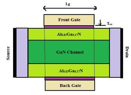
The ID Vg output characteristics of a symmetrical underlap DG andDual DGMOS HEMTare observed using Visual TCAD at variation of different lengths of gate voltages(Vg)isvariedfrom 1Vto1.5Vwithapaceof0.05 V with constant drain voltage 1V. The current increases when the gate to source potential is changed because therearemorecarriers,or2 DEG,inthechannel.
Fig 3: ID Vg characteristicofDualDGMOS HEMTat differentgatevoltageswhereLg =(3,4,5)nmwith1nm oxidethickness.
Table-3: DrainCurrentComparisonForDGandDualDG MOS HEMT
Double Gate Dual Double Gate 0.003A/um 0.009A/um 66.67%
Hereweobserved,theeffectofscalingdownofgatelength iscauseoftheincrementindraincurrentandat3nmgate length ID is about 0.009A/um (9A/mm)and at 12nm gate length ID is about 0.003A/um (3A/mm) of two different MOS HEMTs that is Dual DG and DG respectively and at1nm Tox, the drain current of Dual DG is 66.67% more than DG MOS HEMT. Comparing with an existing paper[10]theID is0.0025A/umwhichislowervalue.
A transconductance gives current with directly proportional to its input voltage. Transconductance is the proportion of alteration of drain current to the alteration of gate voltage. Comparing both the MOS HEMTs with different gate lengths and we observed the plot between gatevoltageandtransconductanceinFig.6
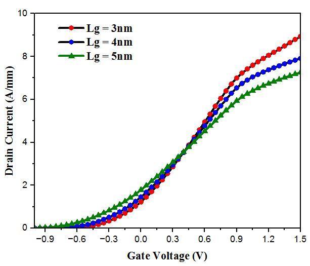
Fig 4: ID Vg characteristicofDGMOS HEMTatdistinct gatevoltageswhereLg =(12,15,18,21)nmwith1nmoxide thickness.
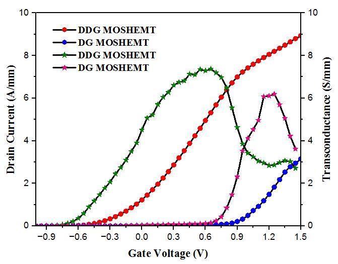
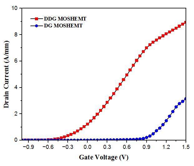
Fig 6: ID Vg andTransconductancecharacteristicofDG andDualDGMOS HEMTat1nmoxidethickness.
Table 4: ObservationofTransconductanceat1nmOxide Thickness Lg=12nm Lg=3nm 6.2×10 3 7.37×10 3
Fig 5: ID Vg characteristicofDGandDualDGMOS HEMT at1nmoxidethickness.
Afterobserving thetransconductancevaluesandtakethe transconductancepeakvaluesofbothMOS HEMTswe foundthatanincreaseintransconductanceiscausedbya decreaseingatelength.Approximately16%higher
International Research Journal of Engineering and Technology (IRJET) e ISSN: 2395 0056
Volume: 09 Issue: 07 | July 2022 www.irjet.net p ISSN: 2395 0072
transconductance of Dual DG MOS HEMT than DG MOS HEMT. The significance of gm is that if more transconductancethenamplificationwillalsogreater.
3.2 Variation of Drain Voltage with respect to Drain Current with different Gate Length and Comparison of conductance values
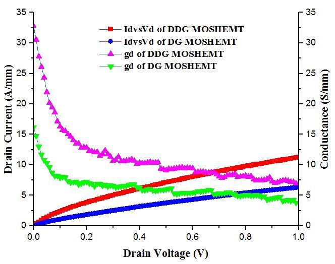
The ID VD features of a symmetrical system's output underlapDGandDualDGMOS HEMTareobservedusing VisualTCADatdrainvoltage(VD)isvariedfrom 0Vto1V with a step of 0.01 V with constant gate voltage (Vg) 0V. When the drain bias is low, when the drain bias is large, thecarrierdensitydependsonthesaturateddrivecurrent, and thelinear drive currentis exactly proportional to the conductance.
Here,Cox istheoxidecapacitanceofdevice,ID isthedrain current, W is the device width, LG is gate length, μn is the electronmobility,VGS isgatetosourcevoltagewhileVDS is draintosourcevoltageandVT isthresholdvoltage.
CapacitanceOxideofthedeviceis, (4)
Where Ɛr= relative permittivity or dielectric persistent of high Kdielectricmaterial,Ɛ0istheconstantpermittivityof 8.854×10 12 F/mandTox isoxidewidthofdevice.
3.3 Comparison of High K HfO2 dielectric with
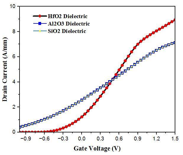
SiO2and Al2O3
High KmaterialssuchasHfO2,ZrO2 andTiO2 havehigh Kvaluesthat ishigher than 3.9.This high k material that is HfO2 is responsible for increase the transistor drive currentandthetransistorswitchingspeed.
Table 5: ValuesofDielectricMaterial
DielectricMaterial ConstantValue
HfO2 25 SiO2 3.9 Al2O3 9
Fig-7: ID VD andconductancecharacteristicofDGand DualDGMOS HEMTat1nmoxidethickness.
A) Model Equations:
The drain current equation of a n channel MOS HEMT in cut offregionis,
ID = 0 Where,[ VGS< VT ] (1)
The drain current equation of a n channel MOS HEMT in linearregionis, (2) Where, The drain current equation of a n channel MOS HEMT in saturationregionis, (3) Where,
Fig 8: Comparison of different dielectric of ID Vg characteristicofDualDGMOS HEMTat3nmgatelengthat differentgatevoltageswith1nmoxidethickness.
3.4 RF Analysis
In this work, we observing the effect of Lg on the small signal RF parameters like cut off frequency (fT), transconductance generation factor (1/V), transconductance (gm) and intrinsic gain (Av) The frequency fT is the one at which the current gain equals one.Amajorroleforhigh speeddigitalapplicationsisthe fT
A) Model Equations:
The proportion of the variation the drain current to the alteration of the gate voltage with constant drain voltage isknownastrans conductance(gm),andtheproportionof the variation of the drain current to the alteration of the drain voltage with persistent gate voltage is known as conductance(gd).
Where, VDS isconstant (5)
Where, VGS isconstant (6)
ForRFapplications,thecut offfrequencyis, (7) (8)
Where, gm is the transconductance and gd is the output conductance CGisthetotalgatecapacitance.
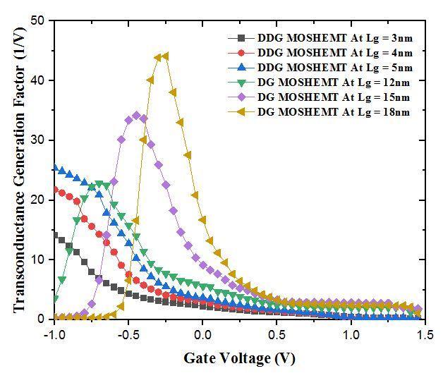
B) DG and Dual DG MOSHEMT Transconductance Generation Factor Comparison
Transconductance generation factor (TGF) is the proportion of gm to ID and is an major parameter for analog applications. TGF determine the available gain Where gm stands for gain and Id stands for consumption. A low TGF means that the capacitive load circuit consumes a lot of power due to the reduced input drive capacity. As Lg decreases ID increases and because this TGFdecreases.
Fig 9: ComparisonofTGFofDualDGandDGMOS HEMT at[3,4,5]nmand[12,15,18]nmgatelengthrespectivelyat differentgatevoltageswith1nmoxidethickness.
Here, we observed that the peak TGF value of DG MOS HEMTis44.1V 1 atLg=18nmandlowervalueof22.5V 1 at Lg=12nm,whileinDualDGMOS HEMTupperTGFvalue is 25.4V 1 at Lg = 5nm and lower value of 14.12V 1 at Lg = 3nm. So reduction in gate length is responsible for reductioninTGFandthisweobservedfromFig.9.
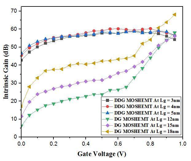
C) Comparison of Intrinsic Gain of both DG and Dual DG MOSHEMT
For circuits like as operational amplifiers, instrumentation amplifiers, and others that call for significantincreases,theinherentgainofaMOSHEMTisa crucial number. You can think of intrinsic gain as the productofgmandRo.
Where, (9)
Fig 10: ComparisonofIntrinsicgainofDualDGandDG MOS HEMTat[3,4,5]nmand[12,15,18]nmgatelength respectivelyatdifferentgatevoltageswith1nmoxide thickness.
Volume: 09 Issue: 07 | July 2022 www.irjet.net p ISSN: 2395 0072
Here, we observed that the peak gain value of DG MOS HEMTis68dBatLg=18nmandlowervalueof56dBat
Lg=15nm,whileinDualDGMOS HEMTuppergainvalue is60.3dBatLg=4nmandlowervalueof59dBatLg=3nm. FromabovevaluationweconcludedthatthegainofDual DG MOS HEMT is bit more than DG MOS HEMT. As we know how much of gate length is decrease then the intrinsic gain is also decrease and this proposed theory plotgraphicallyinFig.10.
D) Effect of Energy Band and Surface Potential in AlGaN/GaN Interface
The valence band of the AlGaN barrier approaches the FermilevelatthesurfacewhenthethicknessoftheAlGaN area is raised. This makes it easier for electrons to move from the AlGaN barrier's valence band to the conduction band of GaN, which leads to a concentration of holes at the surface. As a result, at the surface, a positive sheet charge forms, and at the AlGaN/GaN interface, a corresponding negative sheet charge (2DEG) does the same.
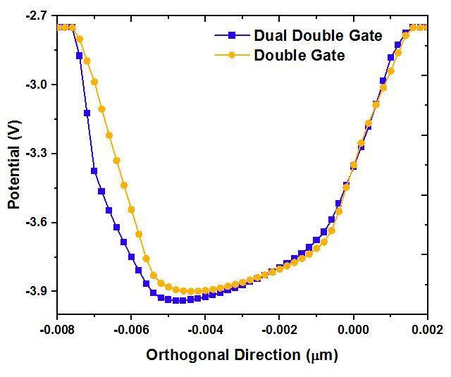
Fig-12: SurfacePotentialdiagramoftheDualDGMOS HEMTandDG MOSHEMTbasedAlGaN/GaN heterostructure.
From above Fig.11&12, the double 2 DEG is present on bothsideoftheAlGaN/GaNinterfaceanditgoesbelowto 0 value and forms corresponding negative sheet charge and the potential of this heterostructure is also comes good.
E) Comparison of Cut-Off Frequency of both DG and Dual DG MOSHEMT
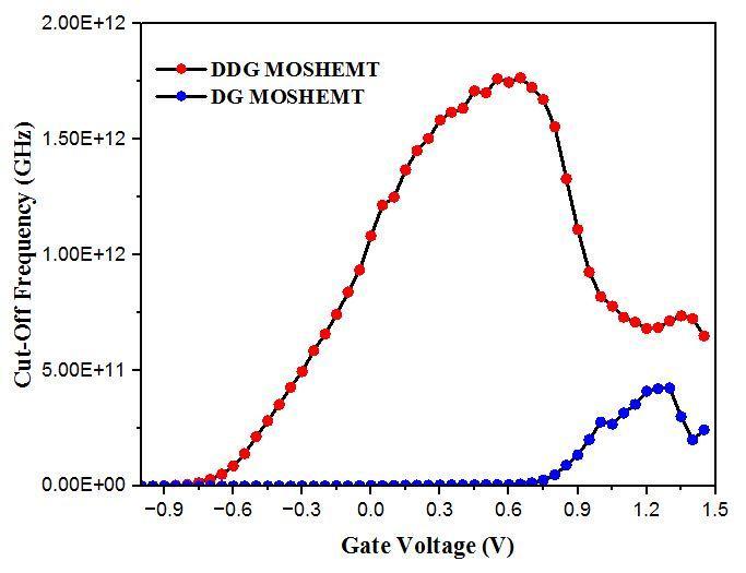
The cut off frequency (fT) is a main parameter for high speed digital applications and for high frequency amplifiertuning.Fordownscalingofdifferentgatelengths ofboththeMOS HEMTsdevicescauseshighfrequency.
Fig 11: BandstructurediagramoftheDualDGMOS HEMTandDG MOSHEMTbasedAlGaN/GaN heterostructure
Fig-13: ComparisonofCut offfrequencyofDualDGand DGMOS HEMTat3nmand12nmgatelengthrespectively atdifferentgatevoltageswith1nmoxidethickness.
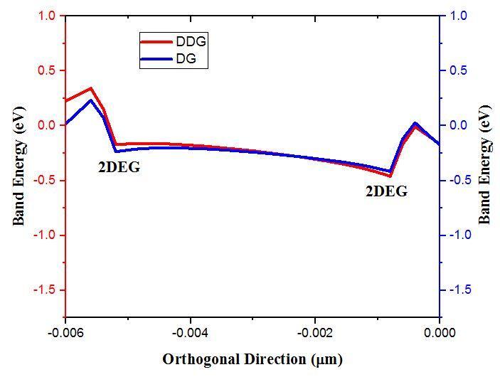
Table-7: Observationof Cut Off Frequencyof1nmOxide ThicknesswithDifferentGateLength
Lg 3nm 12nm 1766.4 424.2
Here,wefoundthatthepeakfT valueofDGMOS HEMTis 424.2 GHz at Lg = 12nm, while in Dual DG MOS HEMT peak value is 1766GHz. So we concluded from TABLE VII. that the downscaling of gate length very important and for this high frequency range it used in modern technologies like in telecommunication sector to prevent interference between different users and it is working at sub millimeterwavefrequenciesuptoTHzrange
4. CONCLUSION
Using Visual TCAD simulation, the Radio Frequency operationofAlGaN/GaNhetero structureDGandDualDG MOS HEMTs is investigated for various types of gate lengths. The newly proposed AlxGa1 xN/GaN Dual DG MOS HEMT heterostructure for observing various RF parameterswithlessgatelengthandcomparedittowith DGMOS HEMT'sparametersandithasalsodifferentgate lengths. In this paper, we observed how a device is more reliable and give better performance by downscaling the gatelength(Lg).Thissimulationresultsspecifiedthat,the AlxGa1 xN/GaN Dual DG MOS HEMT give more drain current at 3nm gate , while DG MOS HEMT obtain this at 12nm gate length of 1nm oxide thickness. However, the AlxGa1 xN/GaN MOS HEMTsrequireDual DG formationto control the SCEs flaw brought on by their small electron effectivemassandnarrowbandgap Agreaterlinearityis achieved by the development of a double 2 DEG at both hetero interfaces, which increases the transconductance with a double hump characteristic. In this work we took 1nm oxide thickness and observed each at different gate lengths.Wefoundthatwhengatelength(Lg)decreasesin the drain current(ID), trans conductance (gm) and cut off frequency (fT) increases. We observed the highest drain currenti.e0.009A/um (9mA/um) at1nmoxide thickness from ID Vg characteristic. The peak transconductance value is 7.37 × 10 3 S/um at 3nm gate length with minimum oxide thickness and for this gm value the cutoff frequency is also higher in number i.e. approx 1766GHz (1.7THz)andforthisthepotentialofusingAlxGa1 xN/GaN Dual DG MOS HEMT is useful device community and for sub millimeter wave antenna application, at defense sectorforcommunicationpurpose.
REFERENCES
[1] Verma, M. and Nandi, A., 2020. Design and analysis of AlGaN/GaN based DG MOSHEMT for high frequencyapplication. Transactions on Electrical and Electronic Materials, 21(4),pp.427 435.
[2] Mitra, R., Roy, A., Mondal, A. and Kundu, A., 2022. Influence of Symmetric Underlap on Analog, RF and Power Applications for DG AlGaN/GaN MOS HEMT. Silicon, 14(5),pp.2329 2336.
[3] Verma, M., & Nandi, A. (2018, January). DC analysis of GaN capped AlGaN/GaN HEMT for different gate drain spacing. In 2018 2nd International Conference on Inventive Systems and Control (ICISC) (pp. 1337 1340).IEEE.
[4] Tschumak, E., R. Granzner, J. K. N. Lindner, F. Schwierz, K. Lischka, H. Nagasawa, M. Abe, and D. J. As."NonpolarcubicAlGaN/GaNheterojunctionfield effect transistor on Ar+ implanted 3C SiC (001)." Applied Physics Letters 96, no. 25 (2010): 253501.
[5] Khan,A.N.,Jena,K.A.N.J.A.L.O.C.H.A.N.,Routray, S., & Chatterjee, G. (2022). RF/Analog and Linearity Performance
[6] EvaluationofLattice matchedUltra thinAlGaN/GaN Gate Recessed MOSHEMT with Silicon Substrate. Silicon,1 10.
[7] Bouguenna, D., Kermas, N. and Djellouli, B., 2015. High performance of cubic AlxGa1 xN/GaN double gateMOS HEMTs. Int Res J Eng Technol (IRJET), 2(9), pp.2072 2077.
[8] Fletcher, A.A. and Nirmal, D., 2017. A survey of Gallium Nitride HEMT for RF and high power applications. Super lattices and Microstructures, 109, pp.519 537.
[9] Panda, D.K. and Lenka, T.R., 2018. Compact thermal noise model for enhancement mode N‐polar GaN MOS‐HEMT including 2DEG density solution with twosub‐bands. IET Circuits, Devices & Systems, 12(6), pp.810 816.
[10] Mukherjee, H., Kar, M., & Kundu, A. (2022). Enhancement in analog/RF and power performance of underlapped dual gate GaN based MOSHEMTs with quaternary InAlGaN barrier of varying widths. Journal of Electronic Materials, 51(2), 692 703.
[11] Pardeshi, H. (2015). Analog/RF performance of AlInN/GaN underlap DG MOS HEMT. Superlattices andMicrostructures, 88,508 517.
[12] Pardeshi,Hemant,etal."Effectofunderlapandgate length on device performance of an AlInN/GaN underlap MOSFET." Journal of Semiconductors 33.12 (2012):124001.
International Research Journal of Engineering and Technology (IRJET) e ISSN: 2395 0056
Volume: 09 Issue: 07 | July 2022 www.irjet.net p ISSN: 2395 0072
[13] Canales, B.G., Carmo, G.J. and Agopian, P.G., 2021, August. The conduction mechanisms analysis of AlGaN/GaN MOSHEMTs with different source/drain electrodeconfigurations.In 2021 35th Symposium on Microelectronics Technology and Devices (SBMicro) (pp.1 4).IEEE.
[14] Ghosh, Sneha, et al. "Study of effective graded oxide capacitance and length variation on analog, rf and power performances of dual gate underlap MOS HEMT." Silicon 14.7(2022):3383 3393.
[15] Baskaran, S., et al. "Impact of High K and Gate to Drain Spacing in InGaAs/InAs/InGaAs based DG MOS HEMT for Low leakage and High frequency Applications." IETE Journal ofResearch (2021):1 11.
[16] Viswanathan, S., Pravin, C., Arasamudi, R.B. and Pavithran, P., 2022. Influence of Interface trap distributions over the device characteristics of AlGaN/GaN/AlInN MOS‐HEMT using Cubic Spline Interpolation technique. International Journal of Numerical Modelling: Electronic Networks, Devices andFields, 35(1),p.e2936.
[17] Sujatha, G., et al. "Noise Characterization of InAs Based Composite Channel DG MOSHEMT with Different Gate Dielectrics." Silicon 14.5 (2022): 1925 1933.
[18] Swain,R.,Jena,K.andLenka,T.R.,2017.Modellingof capacitance and threshold voltage for ultrathin normally off AlGaN/GaN MOSHEMT. Pramana, 88(1),pp.1 7.