International Research Journal of Engineering and Technology (IRJET)
e-ISSN: 2395-0056
Volume: 09 Issue: 07 | July 2022
p-ISSN: 2395-0072
www.irjet.net
Power Efficient 4 Bit Flash ADC Using Cadence Tool Mr. Tilak Kumar L1 Assistant Professor, Department of Electronics and Communication Engineering, Global Academy of Technology, Bengaluru, Karnataka, India Chandan A2, Chethankumar K M3, Dommeti Venkata Sai Krishna Vasanth4, Hemant5 Student, Department of Electronics and Communication Engineering, Bengaluru, Karnataka, India ---------------------------------------------------------------------***---------------------------------------------------------------------
Abstract - ADCs are the essential building blocks of digital
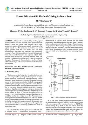
thermometer to binary code encoder are the three components that make up a Flash ADC. The use of a resistor ladder produces several reference voltages. The comparator array compares the incoming analog input to these created reference voltages to produce the associated thermometer code. These thermometer codes are input into the digital encoder, which turns those into the corresponding binary codes.
systems and are now used in a wide range of applications to enhance them and make them perform better than analog alternatives. When analog signals are converted to digital signals and then processed in real-time and mixed signal systems, flash ADC has several uses. For many applications, a high speed and low power ADC is absolutely necessary. The architecture of choice where the highest sample rate and moderate resolution are required is flash ADCs. Despite being the quickest type now available, flash ADC requires a huge number of integrated circuits to implement. Using the Cadence tool, this simulation is performed using 180nm technology. Tabulated simulation results have been documented. Key Words: Flash ADC, Resistor Ladder, Comparator, Encoder; Power Dissipation
1.INTRODUCTION The improvement of integrated circuit technology over the past ten years has sped up the development of digital signal processors. Additionally, digital processing has the benefit of being more noise-resistant. The analog-to-digital converter functions as an interface for both analog signals and the digital signal processing system as a result. Wireless communication systems ongoing speed improvements have led to enormous demands on high-speed, low-resolution analog-to-digital converters power and speed standards.In actuality, processing, testing, and storing of digital signals are made simple. In order to process the analog signal, we convert it to a digital signal. An analog-to-digital converter could be used as the bridge to do this. Researchers are looking into new model strategies for in an ADC in an effort to boost performance while lowering power consumption. Due to the fact that flash ADC design commonly plays a major part in other forms of ADCs, it becomes progressively important in all other forms of ADCs, including pipelined and multi bit sigma delta ADCs.
Fig - 1: Block Diagram of 4-bit Flash ADC Of all ADC types, flash or parallel converters operate at the fastest speed. As seen in Fig. 1 They employ two resistors and one comparator for each quantization level (2-1). (a resistor string DAC). Each of the two values from the reference voltage is put into a comparator. Once the input voltage has been compared to each reference value, the comparators output generates a thermometer code.
Fig-1 illustrates the block diagram for an N-bit Flash ADC. A resistor ladder, a comparator arrangement, and a
© 2022, IRJET
|
Impact Factor value: 7.529
|
ISO 9001:2008 Certified Journal
|
Page 1419