International Research Journal of Engineering and Technology (IRJET) e ISSN: 2395 0056

Volume: 09 Issue: 06 | June 2022 www.irjet.net p ISSN: 2395 0072
International Research Journal of Engineering and Technology (IRJET) e ISSN: 2395 0056
Volume: 09 Issue: 06 | June 2022 www.irjet.net p ISSN: 2395 0072
Department of Electrical and Electronics Engineering,Bapatla Engineering College,Andhra Pradesh,India ***
Abstract - This paper presents a dual inductor based current fedbidirectionalisolatedsnubberlessdc/dcconverter for fuel cell and photovoltaic inverters. This proposed converter provides a higher voltage conversion and zero switch turn off voltage spike without snubber circuit. Most of the dc/dc converters require additional components and snubber for reduce voltage spikes. But in this paper, to eliminate the voltage spike problem by adding soft switching features to the operated converters. Thus, the soft switching technique avoids the need of snubber circuit, voltage across the switches is naturallyclampedandvoltage across switch is independent of the duty cycle. A formal mathematical design parameters are discussed for 300W converter
Key Words: Bidirectional Converter, dc/dc converter , fuel cells, renewable energy sources, soft-switching
Inrecentyearsthegreenenergyandcleanenvironmentis attractedtheattentionofindustriesandcommonmen.With the concept of smart system like smart grid, smart industries,alternativeenergysources,smarttransportation, hybridmicro grid,andefficientsmartpowerconversionis gettingincreasingimportancedaybyday.Alternativeenergy sources(solarPV,Wind)cannotbeuseddirectlybecausethe output isunregulatedandlowpower output. Therefore,a powerconverterisneededtoconverttheiroutputwhichis regulated and high power output. Maximum power from alternativeenergysourcesis extractedandsuppliedto dcgridsandlocalloads.Mainlytheconvertersareusedin solar based electric vehicle charging station due to low power output of the solar PV systems. So, the boost convertersareusedinthisapplicationstoimprovethefuel efficiency,utilizationandthe currentrippleofthefuelcell stack must be minimized [1]. DC/DC conversion is very important in fuel cellor photo voltaic inverters. Several converter topology techniques have been reported [2] [10].Allthesoft switchingconvertertechniquesarestudied andhasjustifiedcurrent fedhalfbridgetopologyissuitable forfuelcellapplications[2] [4].Intheyear2004,theauthors R.Gopinathetal.emphasison
Active clamping zero voltage switching PWM current fed half bridgeisolateddc/dcconverter[11].Anactive clamp helpsinachievingsoftswitchingofdevicesandabsorbsthe
turn offvoltagespikeacrosstheswitches.Anactiveclamp dissipates1%oftheoutputpower.
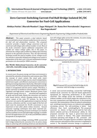
Fig 1:Conventionalhard switchedcurrent fedhalf bridge isolateddc/dcconverter.
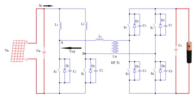
Fig 2:ProposedZCScurrent fedhalf bridgedc/dc converterwithfullbridgeonsecondary.
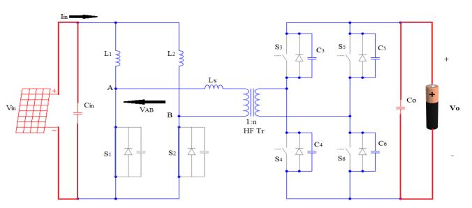
A novel zero current switching current fed half bridge isolated dc/dc converter for fuel cell based applications isproposed for improving performance of the power converter. The voltage across the switches is clamped withoutsnubbercircuitwhichmakesthereductioninsize, lowcost,compactnessandhighefficiency.Intheproposed converter,thecommutationisdonebynaturalcommutation and switchingtransitionlossesarereducedandnegligible circulating current. The soft switching is better load efficiency than hard switching(Fig.1). The proposed converter as shown in Fig.2 can be used for fuel cells, electric vehicles and has a bi directional ability. In this proposed converter the input is given from solar and output is stored in battery. This paper demonstrates converter operation and design of the converter and simulationresults.Thepaperlayoutisasfollows.Operation oftheconverterandanalysisoftheconverterisexplainedin section 2 The detailed converter design is explained in
International Research Journal of Engineering and Technology (IRJET) e ISSN: 2395 0056
Volume: 09 Issue: 06 | June 2022 www.irjet.net p ISSN: 2395 0072
section3.Theproposedconverteranalysisanddesignare verifiedbysimulationresultsusingMATLABinsection4
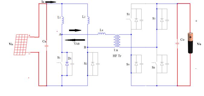
Inthis section,steady stateoperationandanalysiswithZCS high step up dc/dc converter have been explained. The following assumptions are made for converter analysis:1)Boost inductors L1 and L2 are large enough to maintainconstantcurrent.2)Magnetizinginductanceofthe highfrequency(HF)transformerisinfinitelylarge.3)Lsisthe series leakage inductance of the transformer, and all the componentsareideal.TheswitchesofprimarysideS1and S2areoperatedwithgatesignalswhicharephaseshiftedby 180o.The primary side duty cycle is denoted by D and secondarysidedutycycleisdenotedbyds.Here,theprimary sidedutycycleisalwaysgreaterthan50%andsecondary sidedutycycleisalwayslessthan50%.
Theconverteroperationduringdifferentintervalsinahalf cycleisexplainedusingtheequivalentcircuitsshowninFig 3 10.
Interval a (t0<t<t1):In the first interval, primary side switchesS1andS2areconductedandsharing50%eachof the input current. Power is fed to the load by output capacitorandswitchcurrentsandinductorcurrentsarehalf ofthesupplycurrenti.eiL1=iL2=iS1=iS2=Iin/2.
Interval c (t2<t<t3):Inthisinterval,diodeD1oftheswitch S1 starts conducting at t=t2. The currents through the transformerandtheswitchesS2, S4,andS5areincreasing withthesameslope.AttheendofthisintervalcurrentsiLs andiS2reachtheirpeakvalue.Thepeakvaluedependsupon the pulsewidth of the gating signal applied to secondary switches.
Interval d (t3<t<t4):Inthisinterval,secondarysideswitches S4andS5areturnedoffatt=t3.Thecurrentonthesecondary side is taken over by diodes D3 and D6 across secondary switchesS3andS6.
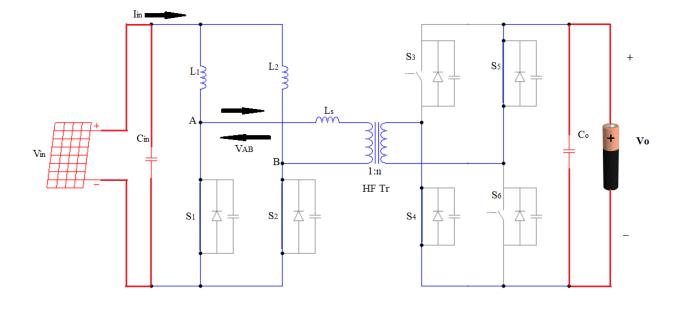
Fig 3
Interval b (t1<t<t2): In this interval, secondary side switches S4 and S5 are turned on at t=t1.It causes voltage Vo/ntoappearacrosstheprimaryofthetransformer, and transformerleakagecurrentiLsstartsbuildingup.Hence,the inductor current iL1,which was earlier flowing through switch S1,is diverted to the primary of the transformer. Therefore,currentiS1 throughswitchS1startsdecreasing linearly,andcurrentiLsstartsincreasing.Attheendofthis interval,switchS1currentreduceszero,causing ZCS turn offsincethegatingsignalhasnotbeenremovedyet.
Interval e (t4<t<t5): Inthisinterval,thesnubbercapacitor acrosstheprimaryswitchS1chargestovoltageVo/n.
International Research Journal of Engineering and Technology (IRJET) e ISSN: 2395 0056
Volume: 09 Issue: 06 | June 2022 www.irjet.net p ISSN: 2395 0072
Interval f (t5<t<t6): Inthisinterval,thetransformerprimary voltage is zero. Therefore, a constant current Iin/2 flows throughitsprimary.switchS2conductsfullinputcurrentIin. Output capacitor C0 is charged by constant current Iin/2n throughthediodesD3andD6.
Interval g (t6<t<t7): During this interval, at t=t6,primary switch S1 is turned on. The snubber capacitor across it dischargesthroughtheseriessnubberresistance,andswitch voltagereducestozeroattheendofthisinterval.
Interval h (t7<t<t8): In this interval, a negative voltage Vo/n appears across the transformer primary, and its primary currentstartsfallingfromIin/2.switchS1current startsincreasing,currentiLsistransferredtoswitchS1.This is the zero current turn on of switch S1.at the end of this interval at t=t8,current iLs reduces to zero, and switch currentiS1increasestoIin/2.
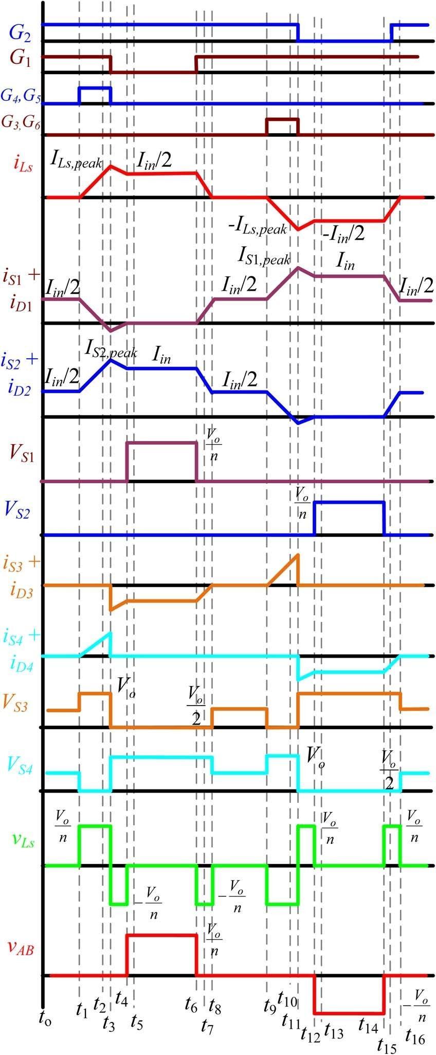
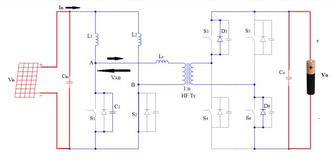
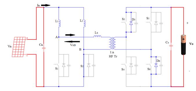
Fig-11: OperatingwaveformsofproposedZCStwo inductorcurrent fedhalf bridgeisolateddc/dcconverter
International Research Journal of Engineering and Technology (IRJET) e ISSN: 2395 0056
Volume: 09 Issue: 06 | June 2022 www.irjet.net p ISSN: 2395 0072
Fig.10
For next half cycle, the intervals are repeated in a similar sequence with other symmetrical devices conducting to completethefullcycle.
In this section, the procedure for converter design is explained by a design example for the following specificationschosenforfuelcellinverterapplication:input voltageVin=24V,Output voltageV0 =350V,Outputpower P0 =300W,andswitchingfrequencyfs=100KHZ.
1)Theaverageinputcurrentis
Assuminganidealefficiency of100%,Iin=12.5A.
2)Themaximumvoltageacrosstheprimaryswitchesis (1)
3)Inputandoutputvoltagesarerelatedas (2)
4)SeriesinductanceLsiscalculatedusing (3)
5)Thermscurrentthroughtheprimaryswitchesisgivenby (4)
6)High frequencytransformerdesign:Thetransformerturn ratio is selected to gain low conduction losses in primary switches. The efficiency of the converter depends upon lossesinprimaryswitchesduetoconductionofhighcurrent.
In HF transformer the losses are copper losses and core losses. The selection of transformer with high turns ratio
requires lower voltage rating switches [using(1)] and low ON stateresistancethisrequirementleadslowerconduction loss.TheleakageinductanceofthetransformerLsdecreases withtheincreaseofturnsratio,thusimprovingthepower transferringcapabilityoftheconverter.Powertransferring ability is limited by the leakage inductance of the HF transformer.Inthisregard,whentheconverterworksinthe reverse direction regenerative braking is happen and absorbstheenergy,smallerleakageinductancewillresultin smallerdutycycleloss.However,higherturnsratioyields higherswitchRMScurrent[from(2)and(4)].Theswitches are selected based on the emerging maximum voltage required for theEVchargers.The maximum valueofduty ratiocorrespondingtoaninputvoltageof24Viscalculated usingequation(2)fordifferentvaluesoftransformerturn ratioandkeepingthesecondarydutyratiods to0.05.Using correspondingON stateresistancetheconductionlossesin primaryswitchesaredetermined.
Theprimaryturnsandsecondaryturnsofthetransformer isdeterminedforvariousturnratios,forallcaseskeepthe maximum flux density in core identical. Gauge winding is selectedbasedonprimarywindingandsecondarycurrents, andwindingresistancesarecalculated.
Here,low costdevicesofsimilarvaluesareselectedbased onvoltagerating.Here,dsissetto0.05.Usingequation(3), theleakageinductanceoftransformerisdeterminedtobeLs =6.22 .Thepeakvoltageacrossthesecondaryswitchesis equal to output voltage V0.Peak and rms values of the transformerprimarycurrentare (5) (6)
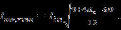
7) ThenecessaryconditionofZCSofprimaryswitchesis (7)
For ensuring ZCS, the value of ds is kept a little higher than the critical value given by equation (7). For this additionaltime,theantiparalleldiodeoftheswitchconducts. However,inordertolimitthecirculating and peakcurrent throughthecomponents,ds shouldnotbehigherthanthe criticalvalue.

8)Boostinductors:Theboostinductorvaluesaregivenby (8)
Where in istheboostinductorripplecurrent.
For in =1A,L=176 H.
International Research Journal of Engineering and Technology (IRJET) e ISSN: 2395 0056
Volume: 09 Issue: 06 | June 2022 www.irjet.net p ISSN: 2395 0072
9) Secondary switches: The peak current through the secondaryswitchesis
(9)
10)Outputcapacitor:ThevalueofoutputfiltercapacitorC0 is (10)
Where V0istheallowablerippleinoutputvoltageandC0= 4.2 Ffor V0=0.5V.ItsvoltageratingisequaltoV0=350V.
Fig 12:Equivalentcircuitduringintervalsaandh
In section 2 steady state analysis of the converter is explained. The devices used in practical converter system haveparasitic.Duetooutputcapacitancetheperformanceof the converter does not change, it slightly transforms the operatingwaveformsduringafewintervals.
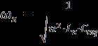
The effect of the output capacitance of the secondary switches is prominent in intervals a and h. At the end of interval h the transformer secondary current reduces to zero.Theequivalentcircuitduringthisintervalisasshown inFig.12.Theresonantfrequencyisgivenby (11)
Where, Ceq is the equivalent capacitance across the secondary side transformer. Considering all device capacitances tobeequal.
Ceq =C3 =C4 =C5 =C6 (12)
During intervalathevoltageacrosstheswitchcapacitances aregivenby
(13)
(14)
Currents through the primary of the transformer iLs and secondaryisec aregiven (15) (16)
In this section, simulation results for a 300W,100KHZ converter design are presented. For this converter Gate pulses G1,G2,G3,G4,G5,G6are triggered for the switches S1,S2,S3,S4,S5,S6respectively.Simulationwasperformedon MATLABtoverifytheanalysisanddesignoftheconverter.
Table 5
In below table the output voltage, current and power are calculated theoretically for different turns ratios for constantcapacitorrating.
Outputvoltageandcurrentvariationsfordifferentnvalues
Turns ratio (n)
Capacitor rating Voltage Current Power
2.5 4.6 F 317 0.93 294.81
3.5 4.6 F 325 0.91 295.75
4 4.6 F 350 0.858 300.05
5 4.6 F 340 0.86 292.4
6 4.6 F 347 0.84 291.48
From the above table, concluded that for different turns ratios output voltage and current are varies but output powerisapproximatelyconstant.Atturnsratio4theoutput voltageishighascomparedwithotherturnsratios.Fromthe aforementioned discussion, designs with n=4 and 4.5 are competitive.However,withlowswitchrmscurrent,i.e.,low lossesandbetterdutycyclerangeforvoltageregulationover wide fuel cell voltage range, n=4 is selected for this application.
International Research Journal of Engineering and Technology (IRJET) e ISSN: 2395 0056
Volume: 09 Issue: 06 | June 2022 www.irjet.net p ISSN: 2395 0072
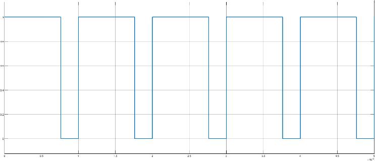
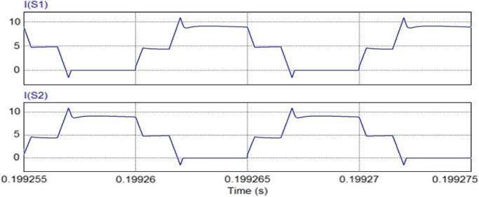
Fig-13:Simulationcircuit
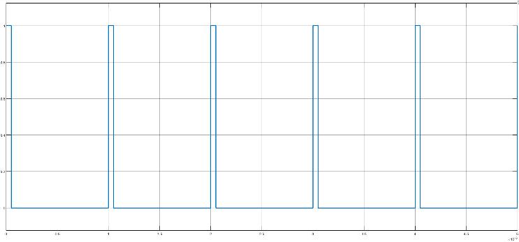
Fig 14:gatepulse(G1)
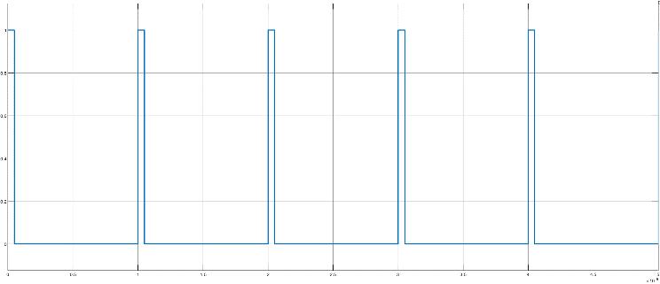
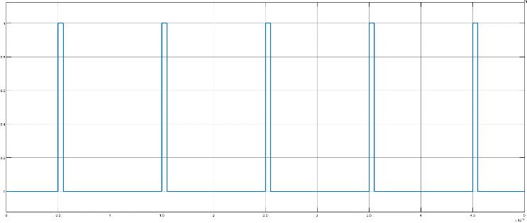
Fig 18:gatepulse(G5)
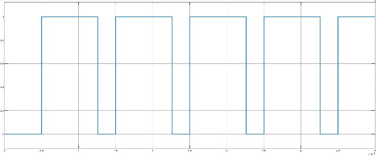
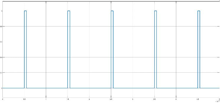
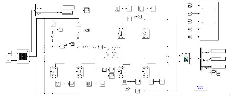
Fig 19: gatepulse(G6)
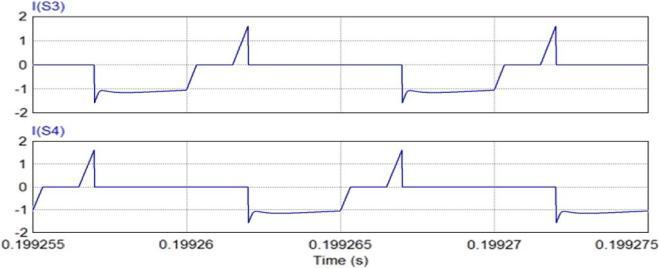
Fig 20illustratesZCSturn offoftheprimaryswitches.The resultsclearlyshowthateachswitchcurrentreacheszero naturallyandtheantiparallelbodydiodeconducts,causinga zerovoltageacrosstheswitch.Therefore,aswitchturn off snubberisnotneeded.Inaddition,thecurrentsthroughthe switchesbuildupwithasloperesultingintheirzero current turn on.
Fig 15: gatepulse(G2)
Fig 16:gatepulse(G3)
Fig 17: gatepulse(G4)
Fig.20.Currentintheprimary sideswitchesshowingZCS turn off.
Fig 21 describes the current through the secondary switches,includingthecurrentthroughtheirbodydiodes. The results show the zero current turn on of secondary switches as the current starts conducting from zero and buildsupwithaslopethatdependsuponthereflectedvalue ofLs.Voltagebecomeszerowheneitherthediodeconducts or the switch is turned on. When switches S4 and S5 are conducting, the voltage across switch S3 is Vo. Voltages acrossalltheswitchesbecomeVo/2,whencurrentthrough the antiparallel diode reaches zero. Fig 22 also shows the voltage across the primary of the transformer. Whenever oneoftheprimaryswitchesisturnedoff,outputvoltageis
International Research Journal of Engineering and Technology (IRJET) e ISSN: 2395 0056
Volume: 09 Issue: 06 | June 2022 www.irjet.net p ISSN: 2395 0072
reflectedacrosstheprimaryofthetransformer.VoltageVAB iszeroduringconductionofboththeprimaryswitch.
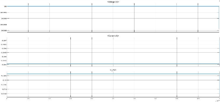
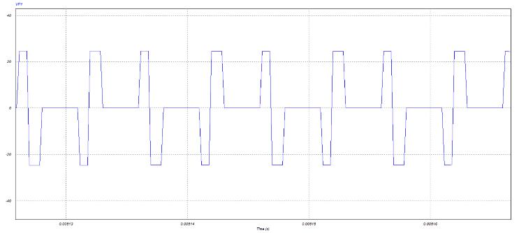
Fig 21:CurrentflowingthroughthesecondarySide switches
Thispaperhasproposedanovelcurrent fedconverterthat providesasecondary side modulation basedsolutionwhich eliminatesswitchturn offvoltagespikeproblem.Becauseof thisrelievestheneed of extra snubbercircuit,makingthe proposed concept novel and snubber less. This reduces component count and peak current through the primary switches, and size of the transformer has been reduced. Voltageoftheprimary sideswitchesisclampedatreflected output voltage. Therefore, a design with selection of low voltage devices is possible. Low voltage and low current devicesarelesscostlyandresultincompactconverters.In addition, such devices have low ON state resistance, resultinginlowconductionlosses,andenhanceconverter efficiencyandmaintainssoftswitchingofallthedevicesas wellasnaturalorzero currentcommutationofbodydiodes ofprimarydevicesaswellassecondarydiodes,resultingin lowswitchinglosses.Steady stateoperation,analysis,and design of the proposed converter have been presented effectivelyandproposedconverterhasbidirectionalpower flowability.Thus,thisconvertertopologyissuitableforlow voltagehigh currentapplicationssuchasfuelcell,PV, and batterysourceapplications.
Fig-22: Voltageacrosstheprimaryofthetransformer
Fig.23 shows the transformer primary current. The simulationwaveformofcurrentiLsmatcheswiththatofthe analysisperformedinSectionII.TheripplefrequencyofiL1 and iL2 is the same as switching frequency fs = 100 kHz. Since these two currents are phase shifted by 180◦ , the ripple frequency of input current Iin is 200 kHz, which is twicetheswitchingfrequencyfs.
[1]S.K.Mazumder,R.K.Burra,andK.Acharya,“Aripple mitigatingandenergy efficientfuelcellpower conditioning system,” IEEE Trans. Power Electron., vol. 22, no. 4, pp. 1437 1452,Jul.2007.
[2]S.Han,H.Yoon,G.Moon,M.Youn,Y.Kim,andK.Lee,“A newactive clampingzero voltageswitchingPWMcurrent fedhalf bridgeconverter,”IEEETrans.PowerElectron.,vol. 20,no.6,pp.1271 1279,Nov.2005.
[3] S. J. Jang, C. Y. Won, B. K. Lee, and J. Hur, “Fuel cell generationsystemwithanewactiveclampingcurrent fed half bridgeconverter,”IEEETrans.EnergyConvers.,vol.22, no.2,pp.332 340,Jun.2007.
Fig 23:Currentacrosstheprimaryofthetransformer
[4]A.K.Rathore,A.K.S.Bhat,andR.Oruganti,“Widerange ZVSactive clampedL Ltypecurrent fedDC DCconverter for fuel cells to utility interface: Analysis, design and experimentalresults,”inProc.IEEEEnergyConvers.Congr. Expo.,2009,pp.1153 1160.
[5]J.Mazumdar,I.Batarseh,N.Kutkut,andO.Demirci,“High frequency low cost DC AC inverter design with fuel cell source home applications,” in Conf. Rec. IEEE IAS Annu. Meeting,2002,pp.789 794.
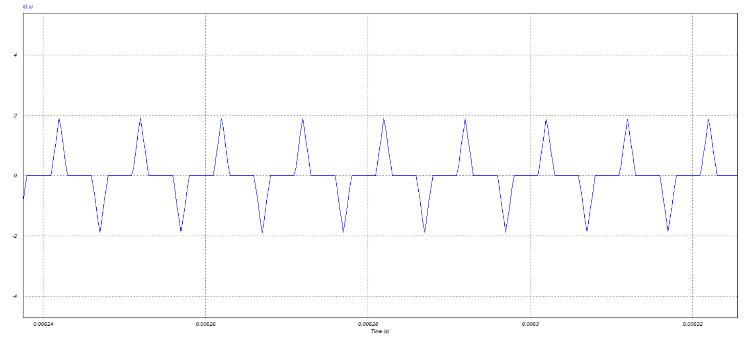
Fig 24:Outputvoltage,outputcurrentandinputcurrent waveforms
[6]Y.J.Song,S.K.Chung,andP.Enjeti,“Acurrent fedHFlink directDC/ACconverterwithactiveharmonicfilterforfuel cellpowersystems,”inConf.Rec.IEEEIASAnnu.Meeting, 2004,pp.123 128.
International Research Journal of Engineering and Technology (IRJET) e ISSN: 2395 0056
Volume: 09 Issue: 06 | June 2022 www.irjet.net p ISSN: 2395 0072
[7] J. Wang, F. Z. Peng, J. Anderson, A. Joseph, and R. Buffenbarger, “Low cost fuel cell converter system for residentialpowergeneration,”IEEETrans.PowerElectron., vol.19,no.5,pp.1315 1322,Sep.2004.
[8]R.Gopinath,S.Kim,J H.Hahn,P.N.Enjeti,M.B.Yeary, and J. W. Howze, “Development of a low cost fuel cell inverter system with DSP control,” IEEE Trans. Power Electron.,vol.19,no.5,pp.1256 1262,Sep.2004.
[9]M.H.Todorovic,L.Palma,andP.Enjeti,“Designofawide inputrangeDC DCconverterwitharobustpowercontrol schemesuitableforfuelcellpowerconversion,”inProc.IEEE APEC,2004,pp.374 379.
[10] M. J. Khan, M. T. Iqbal, and J. E. Quaicoe, “Utility interactive fuel cell inverter for distributed generation: Design considerations and experimental results,” in Proc. IEEECan.Conf.Elect.Comput.Eng.,2005,pp.583 586.