International Research Journal of Engineering and Technology (IRJET) e ISSN:2395 0056

Volume: 09 Issue: 06 | June 2022 www.irjet.net p ISSN:2395 0072
International Research Journal of Engineering and Technology (IRJET) e ISSN:2395 0056
Volume: 09 Issue: 06 | June 2022 www.irjet.net p ISSN:2395 0072
Department of B.Ed, Bijoy Krishna Girls'College, Howrah 711 101 West Bengal, India. Pin: 711 101. ***
Abstract In this report, we have primarily studied the influence of manganese incorporation on structural, optical and ethanol sensing properties of copper oxide ) (CuO thin films synthesized by successive ion layer adsorption and reaction (SILAR) technique. The materials have been characterized using X ray diffraction and optical properties were measured by UV VIS spectrophotometric. Reduction in grain size in doped films up to a certain extent of doping (tentatively 5%) were confirmed from XRD analysis, beyond which there is a reverse tendency. Increase in band gap in doped films were observed up to 5% doping level which could be associated with enhanced carrier density in doped films. Maximum sensitivity of 87% in the presence of 1500 ppm ethanol at the operating temperature 1800C was obtained for 5% doped film.
Keywords: CuO thin film; SILAR; Optical band gap; Ethanolsensitivity.
Nanostructured cupric oxide ) (CuO is one of the important transition metal oxide semiconductor materials having unique optical and electrical properties. CuO has demonstrated its potential in solar cell [1], gas sensor [2 4], superconducting material [5 6], magnetic storage devices[7]andphotovoltaicdevices[8] Thenarrowband gap ofCuO at ~1.2 eV makes it useful for photoconductive andphotothermal applicationsandas an antibacterial agent[9]. Accordingly,besidesitsabundance distribution, chemical stability and environmental friendliness, CuO nanostructures have attracted considerable attention due to its interesting electrical and opticalproperties[10].Variousresearchershavereported these properties forCuO and dopedCuOthin films. The p type conductivity is believed to be due to generation of cation vacancies in the CuO structure [11]. The p type oxides have a tendency to exchange lattice oxygen with air and this is useful in maintaining stoichiometry of the oxides. Another advantage of p type oxides is that
the temperature dependence of conduction in high temperature range is considerably less than that of n typeoxides.Thephysicalandchemicalpropertiesof CuO thinfilmcanbeaffectedbydopingintermsoftheresulting optical, electrical, and structural properties. Influence of various dopants such as zinc ) (Zn , lead ) (Pb , lithium ) (Li and iron ) (Fe on structural, morphological and optical properties of CuO has been reported by various groups [12 15]. Zinc and Nickel doping has been reported to influence the ferromagnetic properties of CuO, the extent of which depends on the amount of dopant ions. Ismail et al, [16] present structural properties of Mn dopedCuOthinfilmspreparedbychemicalspraypyrolysis technique.Rahmanetal.[17]studies bandgaptuningand p to n type transition in Mn doped CuO nanostructured thin films. Zhu et al. [18] describes in their work to structural and magnetic properties of Mn doped CuO thin films, Mustafa et al presents preparation Doped CuO Thin Film and Studies of Its Antibacterial Activity. There is not any report the doping effect on ethanol sensitivity in CuO thin film of manganese ion. Out of number of chemical techniques, CBD is one through which films of thin layers of uniform thickness can be coated on large area. The technique is relatively simple and economic for mass production processes. We have actually adopted successive ion layer adsorption and reaction (SILAR) technique in this work to synthesize Mn thin films which is a modified version of CBD. Both SILAR and CBD involve the same principle where film formation takes place through ion by ion deposition of cations and anions on nucleating sites on the immersed surfaces. While in CBD, deposition of thin films occurs due to substrate maintained in contact with dilute chemical baths containing cationic and anionic solutions together, in SILAR, deposition occurs by immersing the substrate in separately placed cationic and anionic precursors. The onlycommonprobleminCBDisprecipitateformationand wastage of material since the ions combine to form nuclei in the solution also, apart from the substrate. This is avoided in SILAR [8]. Also doping with metal ions at low temperaturescanbeconvenientlycarriedoutusingSILAR technique.
International Research Journal of Engineering and Technology (IRJET) e ISSN:2395 0056 Volume: 09 Issue: 06 | June 2022 www.irjet.net p ISSN:2395 0072
In view of this, the present work was taken up primarily to study the influence on Mn doping on structural, optical and ac electrical conductivity in SILAR synthesized CuOthinfilm.Thus, inthepresentstudy,we have successfully synthesized O Mn Cu x x 1 x( 0.00, 0.01,0.03,0.05and0.07)thinfilmsbySILARmethod.The effect of different doping concentrations of Mn on structural,optical,ethanolsensingpropertiesof CuO thin film has been investigated and compared with those for undoped CuO thinfilms.
CuOthin film was deposited on microscope glass slide substrates cleaned prior to deposition. The substrate was kept overnight in freshly prepared chromic acid solution whichwasfollowedbyrinsingindistilledwaterandfinally ultrasonic cleaning in equivolume mixture of acetone and alcohol.Itwasalternatelydippedinacationicprecursorof copper thiosulphate complex and an anionic precursor of 1.0 M potassium hydroxide solution KOH . The copper thiosulphate complex was prepared by adding sodium thiosulphate 3 2 2 O S Na in copper sulphate O H SO Cu 2 4 2 .5 until a colorless solution results. The cleaned substrate was first dipped in hot KOH solution maintainedat70oCusingaconstanttemperaturebathand then dipped in copper complex solution kept at room temperature.Thedippingtimeineachbathwas5seconds and 25 such dipping cycles were performed to get a uniform thin film. One complete set of dipping involves dipping of the substrate in cationic and anionic precursor respectively. The reaction between 2Cu ion andOH ion takes place on the substrate surface leading to the formation of O Cu2 thin film [19] which on subsequent heat treatment in air at 400oC leads to the formation of CuO film. A thin blight brown adhesive film was formed on the substrate. Manganese doping was carried out by adding appropriate amount of manganese sulphate in cationicprecursor.
Thephaseidentificationandcrystallineproperties of the samples were studied by X ray diffraction (XRD) method with the help of a Bruker (D8 advance) x ray diffractometer using Ni filtered CuK radiation (=1.5418 Å). The diffraction data were recorded in the angular range 20o 80o and the experimental peak positions were compared with standard Joint Committee of Powder Diffraction System (JCPDS) files and Miller
indices were assigned to the peaks. The surface morphology study was performed using FESEM. The absorbance data was measured using double beam spectrophotometer (Shimadzu, UV 1800) at room temperature. The band gap of the films was calculated from the absorption edge of the spectrum. Gas sensing experiments were carried out by placing the sample in a testchambermadeofglass.Copperwireswithconducting silver paste were used for the electrode. Temperature variation was recorded using a sensitive thermocouple placed inside the closed glass test chamber. Change of electrical resistance in the presence of the target gas was measured using at Keithley 6514 DMM set up. Requisite amounts of the target gas were passed over the sample usingaregulatedflowmeter(flowrateof1Lpermin).
Figure1showstheXRDpatternsof CuO andMn doped CuO thin films. Prominent diffraction were peaks observedat~35.94o and~39.16o correspondingto( 111) and (111) diffraction planes which can be associated with monoclinic copper oxide [JCPDS file no. 89 5899]. The other minor peaks at ~32.53o , 49.32o, 54.21o, 58.82o , 62.21o, 66.67o, 68.48o and 75.51o also compares well with monoclinicCuO. The corresponding diffraction planes are (110), (20 2), (020), (202), 3 11 , 1 31 , (220) and 2 22 respectively. The crystallite size was calculatedusingScherer’sformula[20]: cos k D
where k is the Scherrer constant, is the full widthathalfmaximum(FWHM)intensityofthediffraction peakforwhichtheparticlesizeistobecalculated, isthe diffraction angle of the concerned diffraction peak and is the wavelength of X ray used. The average value of crystallite size estimated was found to decrease from ~37.1 nm forCuO to ~25.4 nm for 5% CuO Mn : . The value was however found to increase to ~26.6 nm for 5% CuO Mn : . It is apparent from the figure that the diffraction peaks get broadened with enhancement in dopinglevelupto5%,abovewhichthereisareductionin width of the diffraction peak. Thus, the particle size decreasesuptoa certainlevel of Mn incorporation,above whichthereisareversetendency.
International Research Journal of Engineering and Technology (IRJET) e ISSN:2395 0056
Volume: 09 Issue: 06 | June 2022 www.irjet.net p ISSN:2395 0072

Fig 1: X raypowderdiffractionpatternsofofCuOandMn dopedCuOthinfilm
In order to find a possible reason behind such enhancementinparticlesize,theaverage microstrain inthefilmsweredeterminedusingoftheformula[20]: 4 cos
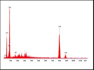
Figure 2 shows the variation of average microstrain and particle size of the samples with doping and they are found to vary in an opposite manner to each other. The strain was found to increase from 3 10 3.72 ~ for CuO to 3 10 6.82 ~ for 5% doping andthenwasfoundtotrimdownto 3 10 15 6 ~ for7%. CuO Mn : Accordinglythereductionofparticlesizeup to 5% doping level might be due enhanced strain leading toenhancedpolycrystallinityinthesamples.
Mnincorporation(%)
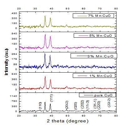
Fig -2:VariationofgrainsizeandmicrostrainCuOand CuO Mn : thinfilms
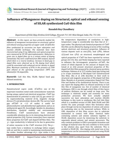
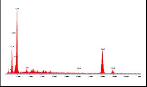
Incorporationof Ni wasalsoconfirmedfromEDX measurement. Figure 3(a) shows the EDX pattern of pure CuOand3(b)for5%Mndoped CuO film. EDXspectrum confirmedthepresenceof Cu ,O andMnelementsinthe deposited film. Some amount of Si was found to be present which appears from the glass substrate used for filmdeposition. (a)
International Research Journal of Engineering and Technology (IRJET) e ISSN:2395 0056
Volume: 09 Issue: 06 | June 2022 www.irjet.net p ISSN:2395 0072

(b)
Fig 3: (a)and(b)showsEDXpatternof CuOand CuO Mn : thinfilms
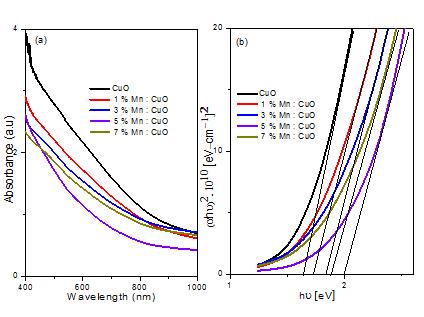
Figure 4 (a) shows the plot of absorbance as a functionofwavelengthforpureanddoped CuO thinfilms in the wavelength range 400 1000 nm. Band gap energy g E wasderivedfromthemathematicaltreatmentofthe data obtained from the absorbance vs. wavelength for direct band gap CuO[21] using the following the relationship:
where is the frequency and h is the Planck’s constant. A is a temperature independent constant for a direct band gap semiconductor and temperature dependent constantforanindirectbandgapone.Fordirectbandgap semiconductor,thisisgivenby[22]:
where o is the electrical conductivity at absolute zero, o n istherefractiveindexand u E istheUrbachenergy.The energy intercept of the plots of 2 h versus photon energy h yields g E for direct transition as shown in figure 4(b). The value of band gap was found to increase with increasing dopant concentration up to 6% doping level.Beyondthislevel ofdoping,thebandgapwasfound
todecrease.Theobservedvalueswere~1.61eVfor CuO anditincreasedto~1.95eVfor5%Mndoping.Thevalue however decreased with further Mn incorporation and it was~1.86eVfor7%Zndoping.Thebandgapvalueswere anaverageofthreemeasurementsindifferentareasofthe film. There was a dispersion of ~0.02 eV about the observed value. The observed result is in contrast to that reported for Mn incorporatedCuO thin films where dopinghasbeenreportedtoreducethebandgap.Rahman et al. [17] on the other hand reported a decrease in band gapinCuO nanoparticles dueto Mndoping.Although no such report on Mn dopedCuO thin films is reported in the literature to the best of our knowledge, such an observation of band gap enhancement with increasing dopinglevel mightbeduetofamiliarBurstein Moss effect [23,24] where carrier density is increased due to dopant incorporation in host semiconductor. Such an effect has been observed for Ni dopedCdO films [25] and In doped CuO[26]. This also indicates that manganese ions substitute copper ions in the lattice structure up to a certain level of doping. Decrease in band gap beyond a certain level of doping might be due to excess manganese ions going to interstitial sites (instead of substitutionally replacingcopperionsinthelatticesites). Fig 4:
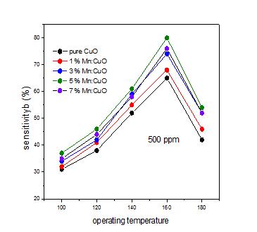
The gas sensing characteristics for fixed concentration of 500 ppm ethanol gas in air was carried
International Research Journal of Engineering and Technology (IRJET) e ISSN:2395 0056
Volume: 09 Issue: 06 | June 2022 www.irjet.net p ISSN:2395 0072
out for all samples. Fig. 5 the variation of percent sensitivity %) (S as a function of temperature. The performance of CuO thin film as a gas sensor is related to the changes in electrical resistance induced by adsorption/desorption of the target gas molecules on its surface.Asairisexposedonfilmsurface,oxygenmolecule gets absorbed on the sensor surface leads to formation of oxygen ion species such as 2 2 ,O O and O ions by trapping electron from conduction band and effectively decrease resistance of the CuO film sensor (increase conductivity).Thisreactioncanberepresentedas
Now when ethanol (reducing gas) is exposed to the sensing film surface, ethanol molecules interact with chemisorbed oxygen species and releasing electrons that recombine with holes as a result decrease electrical conductance which in turn increase the sensor resistance. This mechanism is known as the ionosorption model [27] andthesensingsreactionisgivenby;
g O H g CO ads O ads OH H C 6 ) ( 2 3 ) 2( 2 ) ( 6 ) ( 5 2
g O H g CO ads O ads OH H C 12 ) ( 2 3 ) 2( 2 ) ( 2 6 ) ( 5 2
Percentsensitivity(S%)ofthethinfilmsensorisdefined as %100 airgas air
RR S R
where Rair isthe resistance ofthesampleinairand Rgas is the resistance in presence of target gas. The maximum sensitivity has been achieved at much lower operating temperature of 180oC for 5% doped film thin films. The grain size of the CuO sensor is in the order of few nm, so sensing body consists of pores between the grains. Transport of gas between the pores occur accordingly to Knudsendiffusionequation[28]
Fig- 5: thevariationofpercentsensitivity %) (S asa
functionoftemperatureforallsetofdepositedfilmsof CuO
When ethanol vapor gas exposed on surface thin filmchemisorbedoxygenionspeciesinteractwithethanol moleculesandtherebyreleasingelectronwhichrecombine withholestodecreaseelectricalconductivity.So,itisclear gas sensing is directly proportional to grain size. Moreover,increaseinporosityduetocauliflowerstructure increasestheeffectivesurfaceareaasaresultsreactionof target gas molecules with chemisorbed species increases. As the 30 dipping cycle deposited CuO thin film shows more crystalline with highest grain size and high porosity comparable to others so it shows highest response for ethanol sensing. Temperature dependence of the sensing material i.e., maximum sensing response at operating temperature (180oC) can be understood as follows: at lower temperatures the absorbed ethanol molecule has not get enough energy to overcome the activation energy barrier to react with absorbed oxygen species and at high temperatures gas absorption is too difficult as surface reactivity increased adequately in that temperature. Thus at some in between temperature sensor performance is reachesmaximumvalue[29]
where r is the pore radius, M the molecular weight of the gas,RthegasconstantandTthetemperature.
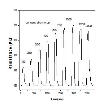
Fig. 6 shows the response and recovery characteristicsof5%dopedfilmatoperatingtemperature inpresenceofdifferentconcentration ethanol gas. Before thetargetgasisexposed,thesensormaterial ispermitted to equilibrate in air at the operating temperature for a certainperiodoftime.Assoonastargetgasisexposed,the resistance increases very sharply initially and then
International Research Journal of Engineering and Technology (IRJET) e ISSN:2395 0056
Volume: 09 Issue: 06 | June 2022 www.irjet.net p ISSN:2395 0072
increases slowly to reach saturation value gas R when reaction between chemisorbed oxygen species and target gasmoleculesiscomplete[30] Fig6showsthegassensing performance increase with increase of concentration of target gas and maximum sensitivity is observed at 1000 ppm, for further increase of gas concentration up to 1000ppm sensitivity remains almost constant. The enhancement in sensitivity with concentration can be explainedfromthefactthathigherconcentrationoftarget gas implies higher number of reactants available for surface reaction and further increase of concentration saturates number of reactants become saturate which in turn saturate sensitivity. The observed response time (timetakenfor90%oftotalresistancereductionaftergas is on) is ~ 50 sec and the recovery time (recovering the initial resistance after gas is off) is ~85sec. The overall sensing performance of the deposited film is good comparable with previous reported literature [31]. Although no systematic results were generated for ammonia and acetone, the material was found to be very low sensitive to 1000 ppm ammonia (8%) and acetone (5%)atmaximumoperatingtemperature.
synthesized by SILAR technique. Manganese could be successfullydopedinCuO thinfilmbythistechnique.The structural,opticalandelectricalcharacteristicsofthefilms were found to be a sensitive function of doping level. Decrease in grain size and enhancement in disorder was found from XRD analysis up to 5% doping, beyond which there is a reverse tendency. Similarly, the band gap in doped films also shows inflexion at this particular level of Mn incorporation. The band gap increase with up to this particular level of doping and then decreases. Incorporation of Mn was confirmed from EDX measurements. 5% Mn doped CuO film shows excellent gas sensing ability with 87% sensitivity for 1000 ppm ethanolatmuchloweroperatingtemperatureof180oC.
[1] K, Han K and M Tao, “Electrochemically deposited p n homojunctioncuprousoxidesolarcells,”SolEnergyMater SolCellsvol 93,2009,pp.153 157
[2]S Steinhauer, EBrunet, TMaier, G Mutinati,A Kock,O Freudenberg, C Gspan, W Grogger, A Neuhold, R Resel, “Gas sensing properties of novel CuO nanowire devices,” SensorsandActuatorsBvol.187,2013,pp.50 57
[3]KattiV,DebnathA,MutheK,KaurM,DuaA,GadkariS, GuptaS,SahniV(2003)MechanismofdriftsinH2Ssensing properties of SnO2: CuO composite thin film sensors preparedbythermalevaporation.SensorsandActuatorsB 96:245 252
[4]ZoolfakarAS,AhmadMZ,RaniRA,OuJZ,BalendhranS, Zhuiykov S, Latham K, Wlodarski W, Zadeh KK (2013) Nanostructured copper oxides as ethanol vapour sensors, SensorsandActuatorsB185:620 627
[5] Zheng X, Xu C, Tomokiyo Y, Tanaka E, Yamada H, Soejima Y (2000) Observation of charge stripes in cupric oxide,PhysRevLett85:5170 5173
Fig 6: showstheresponseandrecoverycharacteristicsof 5%MndopedCuOthinfilmatoperatingtemperaturein presenceofdifferentconcentrationethanolgas.
In the presented work, we have primarily reportedtheinfluenceofMnincorporationonacelectrical conductivity, dielectric relaxation mechanism and impedancespectroscopycharacteristicsof CuO thinfilms
[6]TokuraY,TakagiH,UchidaS(1989)Asuperconducting copper oxide compound with electrons as the charge carriers.Nature337:345 347
[7]FanH,YangL,HuaW,WuX,WuZ,XieS,ZouB(2014) Controlled synthesis of monodispersed CuO nanocrystals. Nanotechnology15:37 42
[8] Jayakrishnan R, Kurian AS, Nair VG, Joseph (2016) MR Effect of vacuum annealing on the photoconductivity of CuO thin films grown using sequential ionic layer adsorptionreaction.MatChemPhys180:149 155
International Research Journal of Engineering and Technology (IRJET) e ISSN:2395 0056 Volume: 09 Issue: 06 | June 2022 www.irjet.net p ISSN:2395 0072
[9]YousefA,BarakatNA,AmnaT,Al DeyabSS,HassanMS, Hay AA, Kim HY (2012) Inactivation of pathogenic Klebsiella pneumonia by CuO/TiO2 nanofibers: A multifunctionalnanomaterialviaone stepelectrospinning. CeramInt38:4525 4532
[10] Khmissi H, Sayed AME, Shaban M (2016) Structural, morphological, optical properties and wettability of spin coated copper oxide; influences of film thickness, Ni, and (La,Ni)co doping.JMaterSci51:5924 5938
[11] Wang C, Fu XQ, Xue XY, Wang YG, Wang TH (2007) Surface accumulation conduction controlled sensing characteristic of p type CuO nanorods induced by oxygen adsorption.Nanotechnology18:145506 14510
[12] Sonia S, Annsi IJ, Suresh PS, Mangalaraj D, Viswanathan C, Ponpandian N (2015) Hydrothermal synthesis of novel Zn doped CuO nanoflowers as an efficientphotodegradationmaterialfortextiledyes.Mater Lett144:127 130
[13] Chand P, Gaur A, Kumar A, Kumar UG (2014) Structural and optical study of Li doped CuO thin films on Si (100) substrate deposited by pulsed laser deposition. ApplSurfSci307:280 286
[14]BayansalF,GulenY,SahinB,KahramanS,CetinkaraH (2015) CuO nanostructures grown by the SILAR method: influence of Pb doping on the morphological, structural andopticalproperties.JAlloyCompd619:378 382
[15]BasithNM,VijayaJJ,KennedyLJ,BououdinaM(2013) Structural, optical and room temperature ferromagnetic propertiesofFe dopedCuOnanostructures.PhysicaELow DimensSystNanostruct53:193 199
[16] Ismail MJ, Khodair ZT, Mahmood MK (2021) structuralpropertiesofMn dopedCuOthinfilmsprepared by chemical spray pyrolysis technique. Materials Today: Proceedings.49:3558 3567.
[17] Rahaman R, Sharmin M, Podder J (2022) Band gap tuning and p to n type transition in Mn doped CuO nanostructuredthinfilms[J].J.Semicond,43(1).
[18]ZhuH,ZhaoF,PanL,ZhangY,FanC(2007)Structural andmagneticpropertiesofMn dopedCuOthinfilms,Appl. Phys.101,09H111.
[19]MustafaAH,SadeerMM,DuhaSA(2018)Preparation Doped CuO Thin Film and Studies of Its Antibacterial Activity,ACTAPHYSICAPOLONICAA135(4).
[20] M. Dhanam, R. P. Rajeev, P. K. Manoj, Mater. Chem. Phys. 107, 289(2008)
[21] Balamurugan B, Mehta BR (2001) Optical and structural properties of nanocrystalline copper oxide thin films prepared by activated reactive evaporation. Thin solidfilms396:90 96
[22]SayedAM,MorsiWM(2013)Dielectricrelaxationand optical properties of polyvinyl chloride/lead monoxide nanocomposites.PolymCompos34:2031 2039.
[23]BursteinE(1954)Anomalousopticalabsorptionlimit inInSb,PhysRev93:632
[24] Mondal S, Bhattacharyya SR, Mitra P (2013) Effect of Al doping on microstructure and optical band gap of ZnO thin film synthesized by successive ion layer adsorption andreaction.PramanaJPhys80:315 326
[25]YakuphanogluF(2011)Preparationofnanostructure Ni doped CdO thin films by sol gel spin coating method. J Sol GelSciTechnol59:569 573
[26] Yildiz A, Horzum S¸ Serin N, Serin T (2014) Hopping conduction in In doped CuO thin films. Appl Surf Sci 318:105 107
[27] Saaédi A, Yousefi R (2007) Improvement of gas sensingperformanceofZnOnanorodsbygroup Ielements doping,J.Appl.Phys.122
[28] Terry PA, Anderson M,Tejedor I (1999) Catalytic dehydrogenation of cyclohexane using coated silica oxide ceramicmembranes,J.PorousMater.6267 274.
[29] Liu J, Wang X, Peng Q, Y. Li (2005) Vanadium pentoxide nanobelts: Highly selective and stable ethanol sensormaterials,Adv.Mater.17764 767.
[30] Zoolfakar AS, Ahmad MZ, Rani RA, Ou JZ, Balendhran S, Zhuiykov S, Latham K, Wlodarski W, Kalantar Zadeh K (2013) Nanostructured copper oxides as ethanol vapour sensors,SensorsActuators,BChem.185620 627.
[31]Gopalakrishna D, VijayalakshmiK,RavidhasC(2013) Effect of annealing on the properties of nanostructured CuOthinfilmsforenhancedethanolsensitivity,Ceram.Int. 39,7685 7691.