International Research Journal of Engineering and Technology (IRJET) e ISSN: 2395 0056

Volume: 09 Issue: 06 | Jun 2022 www.irjet.net p ISSN: 2395 0072
International Research Journal of Engineering and Technology (IRJET) e ISSN: 2395 0056
Volume: 09 Issue: 06 | Jun 2022 www.irjet.net p ISSN: 2395 0072
Monisha J R1 , Dr. S G Srivani2
1PG Student, Department of Electrical and Electronics Engineering, RV College of Engineering, Bengaluru 2Professor, Department of Electrical and Electronics Engineering, RV College of Engineering, Bengaluru ***
Abstract Near Field Communication (NFC) is a short range wireless standard used in data exchange and transaction applications. The NFC standard establishes the connectivity with counterpart with a touch. The NFC technology is evolved from the existing contactless identification and interconnection technologies. This paper presents an NFC system design using NXP PN5190 reader IC. An antenna with symmetrical matching is designed for 13.56 megahertz. The NFC system is designed to operate in Low Power Mode to minimize the current andpower utilization. A Flybackconverterpresentinpower supplyunit ofNFC system isdesignedtooperateforlowpowerapplications.TheFlyback converter achieves an output voltage and output current of 3.3V and 0.1A respectively from the input supply of 12V. The NFC system designed finds its application in access control, point of sale (POS) and Internet of things (IOT).
Key Words: Near Field Communication (NFC), Low Power Mode, proximity, Radio frequency Identification (RFID), Load Modulation, Rectangular Antenna
NearFieldCommunication(NFC)isawirelessstandard fordatatransmissionwithinashort rangeathighfrequency based on Inductive coupling. This technology has evolved from existing Radio frequency Identification (RFID) technology.Thistechnologyisoptedwhenthereisaneedto transfer data immediately and fast. The basic principle of operation is “touch to communicate” which indicates that bringingNFCenableddevicesincloseproximitytoeachother establishes connection for data transmission. The transmissionrangeoftheNFCstandardiscloseto10cmand frequencyofoperationis13.56megahertz.Therateofdata transmissionofferedbyNFCisintherangeof106Kbit/sto 424Kbit/s[1] [8].
TheNFCcomprisesofapollerandatleastonelistener. Thepoller/initiatorhastheabilitytopowerupthepassive listener/target device by generating RF field actively. The NFCtechnologyallowsanNFCenableddevicesuchasmobile to accept data from a tag that is in close proximity to the poller.TheNFCpassivetagconsistsofasiliconchipandan antenna.Thepassivetagdoesnotcontainaninternalpower sourceratheritmakesuseoftheRFfieldgeneratedbythe reader to power up its inner circuitry. The average power consumptionoftheNFCsystemisincreasedduetoreadingof suchpassivetag[1] [8].
NFCisjustnotaninterfacetoexchangedata butalso provides a way to transfer energy to the communication partner called the transponder. Communication with such transponderincreasestheaveragepowerconsumptionofthe systemconsistingofNFCReader,Wirelesscommunication channelandatransponder.TheNFCfindsitsapplicationin lock/unlock andignitecar,payments,transportation,door accessetc.
TheintegrationofNFCintodeviceshasthedrawbackof increasingthedevice’senergyconsumption.Especiallywhen theNFCReaderisasmartphone,duringthereadingprocess theaveragepowerconsumptionofNFC Readerincreasesby upto107%.
UsingNFCsystemsforapplicationslikewirelesspayment, itismandatorytoaddsecurity.Alltheweakspotsmustbe securetopreventattackersfromgainingunauthorizedaccess to the system. To secure the wireless transmission, encryption algorithms like Advanced Encryption standard (AES)canbeused.Theusageofsuchalgorithmsleadstoan increasedenergyconsumptionduringtransmission.
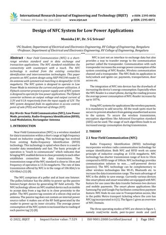
Radio Frequency Identification (RFID) technology incorporateswirelessradiocommunicationtechnologyfor unique identification. Both NFC and RFID work on same principle of inductive coupling at 13.56 megahertz. NFC technologyhasshortertransmissionrangeof4cmto10cm comparedtoRFIDrangeof100cm.NFCtechnologyprovides communication solution to non self powered device (passive). The NFC technology can be complementary to other wireless technologies like Wi Fi, Bluetooth etc. to increasethedatatransmissionrange.Themainadvantageof NFCistheabilitytosaveenergy.Currentlyvariousdevices likesmartphoneandsmartwearablesareequippedwithNFC featureforusecaseslikedatatransferbetweentwodevices and mobile payments. The smart phone applications like SamsungPayandGooglePayfacilitatescontactlesspayment feature.NFCfindsitsusecaseinTransportationaccess,like in the publicMetro transport ticketing where the coinhas NFCtagincorporatedinit[1].Thefigure1givesanoverview ofNFCDomain.
ThethreeoperatingmodesofNFCareshowninfigure1, namely read/write mode, peer to peer mode and card
International Research Journal of Engineering and Technology (IRJET) e ISSN: 2395 0056
Volume: 09 Issue: 06 | Jun 2022 www.irjet.net p ISSN: 2395 0072
emulation mode. The Card Emulation Mode consists of an active NFC reader and a Passive NFC card in the communicationsetup.TheNFCreaderreadstheinformation stored in the passive tag. In Read/Write Mode the NFC enableddevicecanreaddatafromtagorwritesinformation totheNFCtag.TheNFCtagispoweredbythemagneticfield andsendsresponsetotherequest.InPeer toPeerModetwo NFCenableddevicescommunicatewitheachother.ThePeer to Peermodeenablesdevicestoconnectandinteractwith each other to exchange data, money transfer and social networking.
The critical issue in embedded devices is the power utilizationduetowhichthereisaneedforextendedbattery life.Thetwoscenariosinwhichsystemspowerconsumption canbeconsideredarewhenthesystemisinuseandwhen thesystemisinidlestate.Thesolutiontothisproblemisthe deployment of the low power CPU modes. The power managementinembeddedsystemscanbeachievedeitherby firmwarepowermanagementorperipheralpowerdown.
Firmware Power management The two measures firmware can into consideration to keep the power utilization minimum are to switchoffthesystemperipheralswhenitisnot inuseandtoregulatethevoltageandfrequency oftheCPUbasedontheperformanceneeds.
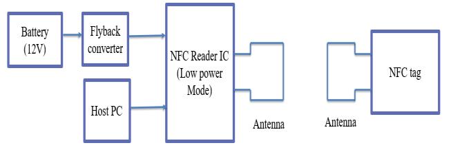
The basic NFC System is shown in figure 2. The NFC systemconsistsmainlyofthreecomponents aTag,aReader and a Controller. A Tag, also called a pulse transceiver consists of a semiconductor chip and an antenna. An electronic control module, RF module and an antenna is presentinthereaderdevice.Acontrollercomponentofthe NFCsystemisusuallyaPC[1].
NFC communication establishment involves three activities
PowertransferforcommunicationbyRFfieldof theNFCReader.
Modulationofthefield.
LoadModulationofthefield.
Peripheral Power Down The very common approachtosaveenergyinembeddedsystemis to switch it off. The complete system turn off whennotinuseisnotrecommendedbecausea fullypowereddowndevicemaytakesometime tostartup.So,theembeddedsystemshouldbe designed such a way that the peripherals and subsystemsmaybeturnedonoroffbyfirmware temporarily. Therefore, an alternate to the systempowerdownisthelowpowermodes.
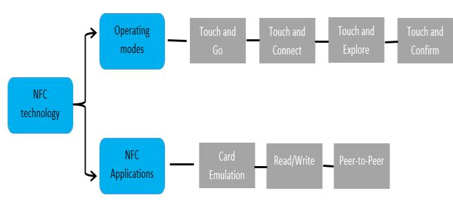
The proposed NFC reader include low voltage power domains into their architecture and offer when it is associatedwithpowermodes,embeddedpowerstates.The low power mode of operation to reduce the energy consumptionischosenbyacommandinapplicationrunning onthesystem[2].
TheBlockdiagramoftheNFCSystemproposedisshown infigure3.
The tag and a reader in the NFC system have radio frequencycommunicationbetweenthem.Eachtagconsistsof unique identification number and an antenna. The NFC Reader will use unique identification number of the tagto
International Research Journal of Engineering and Technology (IRJET) e ISSN: 2395 0056
Volume: 09 Issue: 06 | Jun 2022 www.irjet.net p ISSN: 2395 0072
establish communication. The read distance of the NFC reader dependent on the antenna parameters such as the shape, size, frequency etc., surrounding environment and others[1].

The NFC Reader communicates with host PC via host interfaces,whichcanbeeitherofI2C,SPI,USBorserialUART. In the proposed system the Reader IC is considered to be PN5190IC.ThereaderICcanbecustomizedtooperateinlow powermodeinorderminimizecurrentconsumptionviaa softwareapplicationflashedontoit.Thevariouslowpower modesinwhichreaderICcouldoperatearesuchasStandby mode, Suspend mode and ultra low power card detection mode. The reader IC have several other features and interfaces accommodated in the chip to meet the requirements of different use cases. The NFC Reader comprisesofanantennawhichischosentoberectangular patch antenna. The main issue in the design of the NFC systemistheantennaalignmentwiththereader[1].

Thechoiceofrightantennadependsontheapplication requirements.Intheprocessofchoosingtherightantenna therearetradeoffsbetweenapplicationsrequiringmaximum readdistance(consumeslargepower)andapplicationswith strict power budgets (results in short read range). The balancebetweenthetwoextremescanbeachievedwitha blendofpowerefficiencyandperformance,whichcanbemet withthelatesthigh performancereadersfeaturingultra low powercarddetection.Intheproposedsystemarectangular antennaischosenbecauseitisasymmetricalantennawith equalpowerdistribution.Thebillofmaterialandthenumber ofcomponentsisreduced.Thefigure4givesanexampleof rectangular antenna and dimensions. The inductance of antennacanbecalculatedusingfollowingformulas:
(1)
(2) (3)
(4) (5)
where: =lengthinmm =widthinmm =trackthicknessinmm w=trackthicknessinmm =numberofturns
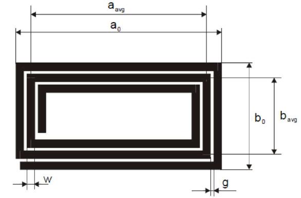
Theabove mentionedparametersarecalculatedtodesign anantennaforNFCreader.Theantennadimensionsare = 45mm, =45mm, =3,w=200µm,g=400µm,t=35µm. Theinductancevalueofanantennaobtainedbytheabove mentionedequationsis1.2837µH.
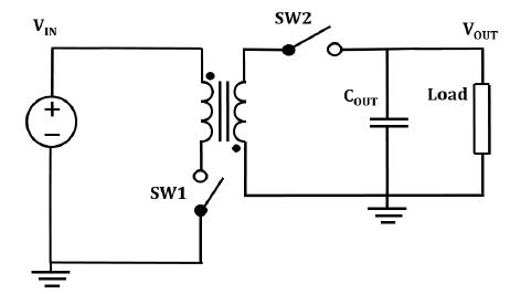
ThepowersupplyunitoftheNFCsystemcomprisesofa batteryof12Vandaflybackconverterhasbeenincorporated forDC DCconversion.Theflybackconverterwillstepdown thebatterysupplyvoltageto5V/3.3V.Theflybackconverter is a DC DCconverter topology like boostconverter having similar structure and performance. The converter stores energywhencurrentflowsusinganinductorandsupplies energywhenthepowerisremoved[9].
Flyback switch mode power supply is most commonly used SMPS circuit for low output power applications. The flybackconverterhastwooperationphases:whenthepower frominputsideisbeingtransferredtotheoutputwhenthe primarysideswitchisoffandwhentheprimarysideswitch isonandtheoutputdonotreceivepowerfromprimaryside. The basic flyback design has few low cost material requirements just like the other dc dc converters: the capacitor,theMOSFETastheprimaryswitch,thediodeasthe secondary switch and inductor is being replaced by the
International Research Journal of Engineering and Technology (IRJET) e ISSN: 2395 0056
Volume: 09 Issue: 06 | Jun 2022 www.irjet.net p ISSN: 2395 0072
flyback transformeror simplytransformer [9].Thesimple flybackconvertercircuitryisshowninFigure5.
The necessary equations required for the design of the flybackconverteraregivenbelow.Thedutycyclecalculation oftheconverterisrequiredtodeterminetheconductionratio ofthecircuitTheconverterisdesignedforanoutputvoltage of 3.3V from an input voltage of 12V. The duty cycle calculatedfromthebelowmentionedequation(9)is45%.
Thetransformerratio ,inthisdesignissetas3.
TheloadresistanceRcalculatedwiththeoutputcurrent of0.1Ainequation(10)is33

Intheconverterdesigntheswitchingfrequencyis takenas100KHzwithIminas0.06A.Thevalueof inductanceLcalculatedin(11)is22.5mH.
ThecomputedvalueofcapacitanceCin(12)is6.81µF.
The simulation circuit of flyback converter using PSIM toolisshowninFigure6.
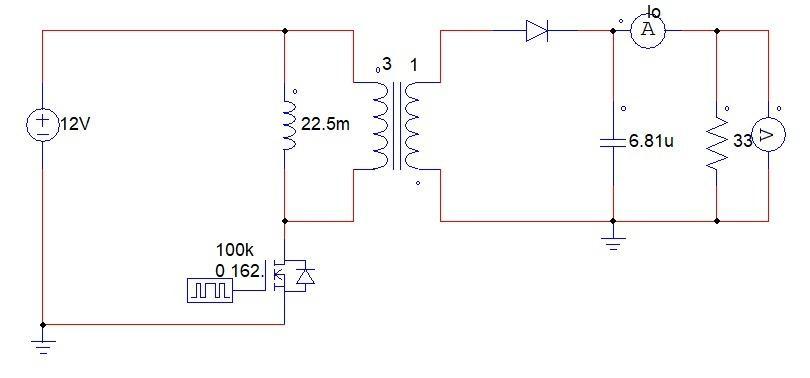
Theschematicoftheflybackconvertercomprisesof aMOSFET,whichactslikeaswitch,atransformer,adiode operating complementarily to MOSFET, an inductor and a capacitor.Thepulsegeneratormoduleisusedforthecontrol ofdutycycleofthecircuitbyturningonandofftheMOSFET switch.Theconvertercircuitcomponentsarepositionedto achievethedesiredoutputconditionof3.3Voutputvoltage and0.1Acurrent.
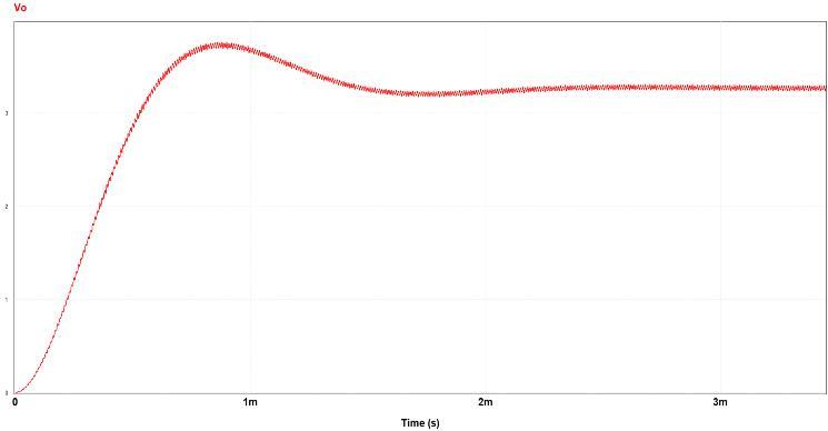
The waveforms generated by the designed flyback converter are shown below. The figure 7 depicts the waveformof3.3Voutputvoltageobtainedbythedesigned converter circuit.
2022, IRJET | Impact Factor value: 7.529 | ISO 9001:2008 Certified
International Research Journal of Engineering and Technology (IRJET) e ISSN: 2395 0056
Volume: 09 Issue: 06 | Jun 2022 www.irjet.net p ISSN: 2395 0072
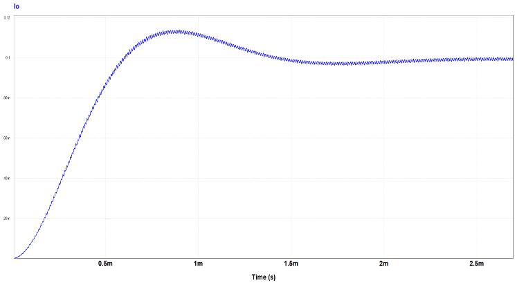
The output current of 0.1A waveform is as shown in Figure8.
[4] Marti Boada, Antonio Lazaro, Ramon Villarino, David Girbau, “Battery Less NFC sensor for pH Monitoring”, 2018 in IEEE Access, vol. 7, pp. 33226 33239, doi: 10.1109/ACCESS.2019.2904109.
[5] Ashish Gupta, Sankaran Menon, Chinna Prudvi, Rolf Kuehnis, Sukhbinder Singh Takhar, Spencer Millican, EricRentschler,PandyKalimuthu,PreetiRanjanPanda, Priyadarshan Patra, “Techniques for Debug of Low powerSOCs”,in201920thInternationalWorkshopon Microprocessor/SoC Test, Security and Verification (MTV)IEEE,doi:10.1109/MTV48867.2019.00017.
[6] Cai Lijin, Liu Cifang, Tang Jingpeng, Liang Honglian, “Design and Implementation of Portable Terminal Power Management System Based on ARM”, in Proceedings 2013 International Conference on Mechatronic Sciences, Electric Engineering and Computer(MEC),doi:10.1109/MEC.2013.6885334.
Fig -8:OutputCurrentWaveform
An NFC system design has been proposed, which incorporates an antenna operating at 13.56MHz. A rectangularantennawithinductanceof1.2837µHhasbeen designed. The power supply unit of the proposed NFC system incorporated a flyback converter. The flyback converterdesignispresentedandsimulatedinPSIMtoolto obtain an output of 3.3V with output current 0.1A from supplyof12V.Theswitchintheflybackconverterconducts for0.45dutyratio.Theflybackconverterisaviablechoice for use cases requiring low voltage and power such as a portabledevice.Thecreditpayments,datatransfer,access controlandvendingmachinesarethevarioususecasesof theproposedNFCsystem.
[1] Stanyo Kolev, “Designing a NFC system,” 56th International Scientific Conference on Information, CommunicationandEnergySystemsandTechnologies (ICEST),2021.
[2] Y van Debizet, Guenole Lallement, Fady Abouzeid, Philippe Roche, Jean Luc Autran, “Q Learning based AdaptivePowerManagementforIoTSystem on Chips with Embedded Power States,” in 2018 IEEE International Symposium on Circuits and Systems (ISCAS),DOI:10.1109/ISCAS.2018.8351385.
[3] Fernando Paixao Cortes, Juan Pablo Martinez Brito, EvertonGhignatti,AlfredoOlmos,FernandoChavezand Marcelo Lubaszewski, “A Power management system architectureforLFpassiveRFIDtags”,in2014IEEE5th LatinAmericanSymposiumonCircuitsandSystems,doi: 10.1109/LASCAS.2014.6820279.
[7] ZhuJing,LuFeng, “System LevelPowerManagementfor Low Power SOC Design” in 2011 10th International SymposiumonDistributedComputingandApplications to Business, Engineering and Science, doi: 10.1109/DCABES.2011.87.
[8] DayingSun,ShenXu,WeifengSun,ShengliLu,Longxing Shi, “Low Power Design for SoC with Power Management Unit”, in 2011 9th IEEE International Conference on ASIC, DOI: 10.1109/ASICON.2011.6157306.
[9] MelissaBMartin,“ADesignof3.3WClosedLoopFlyback Converter with 3.3V, 1A Output for Low Voltage Applications,”IEEE8th ConferenceonSystems,Process andControl(ICSPC),2020.
© 2022, IRJET | Impact Factor value: 7.529 | ISO 9001:2008 Certified Journal | Page1845