International Research Journal of Engineering and Technology (IRJET) Volume: 09 Issue: 06 | June 2022
e-ISSN: 2395-0056
www.irjet.net
p-ISSN: 2395-0072
Design and Analysis of SEPIC Converter for Battery Charging Applications – Part I – Simulation Studies Siddalingaradhya H M1, Nalini S2 1PG
Student, Department of EEE, Dr.AIT, Bengaluru, Karnataka, India Professor, Department of EEE, Dr.AIT, Bengaluru, Karnataka, India ------------------------------------------------------------------------***------------------------------------------------------------------------ABSTRACT – In this paper, the design of sepic converter II SEPIC CONVERTER: 2Associate
for battery charging applications is presented. The design procedure of sepic converter is analysed and its operation under varying input voltage is studied. A voltage regulation control circuit is added with PI controller and the results are studied with different reference voltages. The results of the proposed inverter is provided with MATLAB/Simulink software.
I.
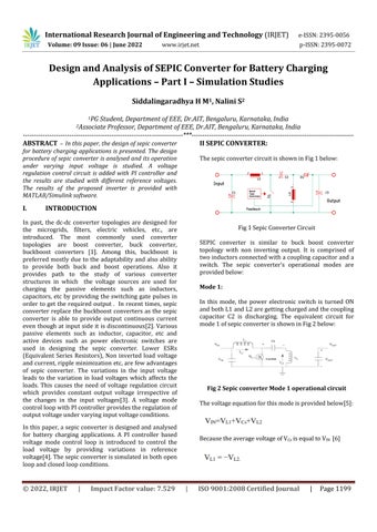
The sepic converter circuit is shown in Fig 1 below:
INTRODUCTION
In past, the dc-dc converter topologies are designed for the microgrids, filters, electric vehicles, etc., are introduced. The most commonly used converter topologies are boost converter, buck converter, buckboost converters [1]. Among this, buckboost is preferred mostly due to the adaptability and also ability to provide both buck and boost operations. Also it provides path to the study of various converter structures in which the voltage sources are used for charging the passive elements such as inductors, capacitors, etc by providing the switching gate pulses in order to get the required output . In recent times, sepic converter replace the buckboost converters as the sepic converter is able to provide output continuous current even though at input side it is discontinuous[2]. Various passive elements such as inductor, capacitor, etc and active devices such as power electronic switches are used in designing the sepic converter. Lower ESRs (Equivalent Series Resistors), Non inverted load voltage and current, ripple minimization etc, are few advantages of sepic converter. The variations in the input voltage leads to the variation in load voltages which affects the loads. This causes the need of voltage regulation circuit which provides constant output voltage irrespective of the changes in the input voltages[3]. A voltage mode control loop with PI controller provides the regulation of output voltage under varying input voltage conditions.
Fig 1 Sepic Converter Circuit SEPIC converter is similar to buck boost converter topology with non inverting output. It is comprised of two inductors connected with a coupling capacitor and a switch. The sepic converter’s operational modes are provided below: Mode 1: In this mode, the power electronic switch is turned ON and both L1 and L2 are getting charged and the coupling capacitor C2 is discharging. The equivalent circuit for mode 1 of sepic converter is shown in Fig 2 below:
Fig 2 Sepic converter Mode 1 operational circuit The voltage equation for this mode is provided below[5]:
In this paper, a sepic converter is designed and analysed for battery charging applications. A PI controller based voltage mode control loop is introduced to control the load voltage by providing variations in reference voltage[4]. The sepic converter is simulated in both open loop and closed loop conditions.
© 2022, IRJET
|
Impact Factor value: 7.529
Because the average voltage of VCs is equal to VIN [6]
|
ISO 9001:2008 Certified Journal
|
Page 1199