International Research Journal of Engineering and Technology(IRJET) e ISSN: 2395 0056

International Research Journal of Engineering and Technology(IRJET) e ISSN: 2395 0056
Soumya K1 , Arpitha Raju B2 , Bhanuprakash CV3, B.K Singh4
1PG Student, Department of EEE, Dr.AIT, Bengaluru, Karnataka, India
2Assistant Professor, Department of EEE, Dr.AIT, Bengaluru, Karnataka, India
3 Assistant Manager, Centum Electronics, Bengaluru, Karnataka, India 4 Director, Centum Electronics, Bengaluru, Karnataka, India ***
Abstract Forward converter is preferred for designing the power supply unit in space application due to its simple structure and provides perfect isolation between input and output. Design and implementation of lesser weight, compact size, high effective single output DC DC converter for space application. The switching frequency of 500 kHz is selected to reduce the size of the converter with PWM Controller UC2825 and Feedforward Technique is used. The inhibit is used to turn off the converter manually and LCD snubber is used to reduce the stress on MOSFET. The proposed converter drives 5V/8A from the Input voltage of 18 50 volts range. The efficiency greater than 76% with output power of 40W.
Key Words: Forward Converter, Inhibit, Input voltage feed forward, LCD snubber, UC2825 PWM IC.
DC-DC Converter is designed to be backward compatible in addition of an output voltage adjustment pin for the single outputmodels.Theseconvertersareradiationhardened,theirlessersizeandlessweightmakethemidealforapplications such as geostationary earth orbit satellites and deep space probes. They demonstrate a high tolerance to the environmental changes happen in the space. The converter has a fixed frequency with the single output and forward topology is used with magnetic feedback. Forward converter opts for designing the power supply unit due to its simple structureandgivesperfectisolationbetweeninputandoutput.Theswitchingfrequencyof500kHzisselectedtodecrease thesizeoftheconverterwithPWMControllerUC2825andFeedforwardTechniqueisused.Theinhibitisusedtoturnoff the converter manually and LCD snubber is used to reduce the stress on MOSFET, start-up circuit is used to generates initial voltage for PWM Controller circuit of forward converter. Feedforward voltage topology is being used for fast response of closed loop control with change in line voltage on primary side of forward transformer, input side has protection circuits such as Over voltage protection(OVP), Under voltage protection(UVP), Over current protection(OCP), Shortcircuitprotection.TheSecondarysidevoltageisrectifiedandfilteredtogive5V/8Aregulatedoutputwithpowerof 40W
Inputvoltage: 18Vto50V.
OutputVoltage: 5V/8A.
Outputpower: 40W
Efficiency: >75%
SwitchingFrequency: 500KHz
Ripple: <50mV
Lineregulation: 5V:±10mV
LoadRegulation: 5V:±25mV
Synchronization: 450KHzto550KHz
Operatingtemperature: 55ºCto+85ºC
Volume: 09 Issue: 05 | May 2022 www.irjet.net p ISSN: 2395 0072 © 2022, IRJET | Impact Factor value: 7.529 | ISO 9001:2008 Certified Journal | Page3165
International Research Journal of Engineering and Technology(IRJET) e ISSN: 2395 0056
Volume: 09 Issue: 05 | May 2022 www.irjet.net p ISSN: 2395 0072
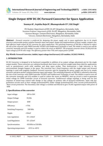
ThesingleoutputDC DCConverterisdesignedandrealizedbasedonthespecificationsgivenbytheCustomer.Theabove figureshowsthedetailedblockdiagramofthepowersupply.Thepowersupplyhassingleisolatedoutputs(5V/8A)which isrealizedusingForwardconvertertopology,InputBusvoltage18V 50VrangeissuppliedtoEMIfillerwhichisdesigned tomeetthedifferentialmodeConductanceEmissionandConductanceSusceptibilitytestsrequirement.Filteredoutputis providedtoprimarysideoftheforwardtransformer.start upcircuitprovidebeginningvoltageforPWMControllercircuit of forward converter. PWM Controller turns ON and Driver IC gets on and initiates GATE Pulses at switching frequency (500KHZtooptimizethesize)toPrimarysideMOSFET.WiththisswitchingactionofMOSFET,InputBusvoltageisapplied toForwardtransformerandenergizesitandmagneticfeedbackisused[5].
Feedforwardvoltagetopologyisbeingusedforfastresponseofclosedloopcontrolwithchangeinlinevoltageonprimary side of forward transformer, Bias winding is used to originate the bias voltage to power the controller circuits. The bias winding voltage is greater than the start-up circuit voltage so that a PWM controller circuit starts drawing the current from the bias winding instead of the start-up circuit [1]. Hence bias winding will act as the House Keeping Bus and will continuetopowerthePWMICandassociatedICs.InputsidehasprotectioncircuitssuchasOvervoltageprotection(OVP), Under voltage protection(UVP), Over current protection(OCP), Short circuit protection. The Secondary side voltage is rectifiedandfilteredtogive5V/8Aregulatedoutputwithpowerof40W.
Areaproductmethodisusedtofindthesizeofapowertransformer[4].
SelectedToroidCore:YP 41605 TC,Ur:2500,AL:1375mH/1000T.
Areaproduct = √ (1)
Where,Windowfactor( )shouldbebetween0.3to0.5
Fluxdensity( )shouldbebetween0.12to0.2forferritecorematerial.
Currentdensity(J)shouldbebetween3Amp/ to6Amp/ = (2)
© 2022, IRJET | Impact Factor value: 7.529 | ISO 9001:2008 Certified Journal | Page3166
International Research Journal of Engineering and Technology(IRJET) e ISSN: 2395 0056
Volume: 09 Issue: 05 | May 2022 www.irjet.net p ISSN: 2395 0072
Turns ratio = (3)
Inaforwardconverter,duringturn offperiodthemaximumvoltagewillbemeasuredacrosstheMOSFET willbethetice ofthemaximumofinputvoltage.SotheMOSFETtakenisSELECTEDMPN:IPP60R125CP,650V,25A,125mOhm,TO220 3 . For safe operation, MOSFET taken should has a breakdown voltage should be more than 3 times the maximum supply voltage[4].
ELECTEDMPN:IPP60R125CP,650V,25A,125mOhm,TO220 3 + (4)
P_conduction=1.25*R_DS*Ip_ (5) P_Coss= (6) P_Switching_ON= (7) P_Switching_OFF= (8)
4.3
Theinhibitisusedtoturnofftheconvertermanually,theinhibitsignalturnofftheconverterwithouthavinginterruptto theinputvoltageandinputcurrentdrawnbytheregulatorisreduced.
Synchronizationcircuitisusedinforwardconverter,ofonefrequencytosyncwiththeotherdeviceofdifferentfrequency. Ifthe two or moreconverteroperateindifferent switchingfrequencyit isdifficulttoanalysisorpredicttheinputripple and it is hard to design the input filter due to the asynchronous operation of different switching frequency, and create harmoniccontentsattheinputDCbuswhichisdifficulttoeliminate.
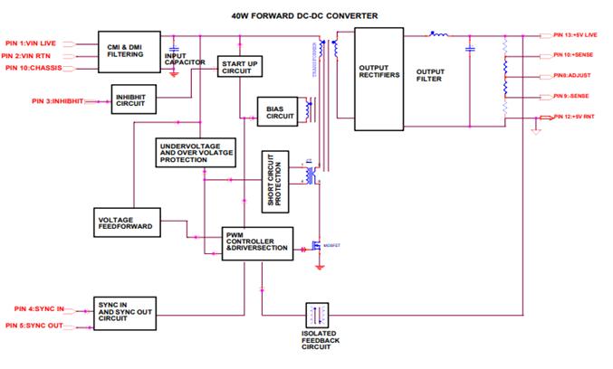
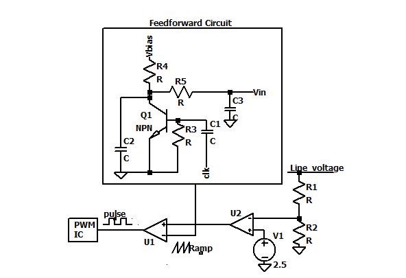
The forward converter operateswiththe wide range of input voltage from 18 50V andwith the varyingload from10% 100%toregulatetheoutputof5V/8A withthefixedswitchingfrequency.ToachievethisthePWMtechnique isused.In voltagecontrol techniquetherearefewdraw backssuchasloopgain isvaried withinputvoltage andscaling isdifficult. Hence the new technique is introduced which is input voltage feedforward technique. In this feedforward technique the error amplifier is connected to the comparator inverting point and at the non inverting point the oscillatory or feedforward circuit is connected, both the error signal and feedforward signal is compared and we get output as pulse whichisconnectedtothePWMICpin.TofeedforwardcircuittheVinhasbeengivensothatthedelayfromerroramplifier canbeavoided,heretherampiscomparedwiththereferenceandwegetoutputaspulsewiththedifferentduty.
© 2022, IRJET | Impact Factor value: 7.529 | ISO 9001:2008 Certified Journal | Page3167
International Research Journal of Engineering and Technology(IRJET) e ISSN: 2395 0056
Volume: 09 Issue: 05 | May 2022 www.irjet.net p ISSN: 2395 0072
Fig 2: circuitandWaveformofVoltageFeedforwardControl
Input side has protection circuits such as Over voltage protection(OVP), Under voltage protection(UVP), Over current protection(OCP).
The over voltage protection is used to avoid the damage of any device from the maximum voltage or over voltage, if the voltage exceeds more than the specification, the components may get damage to avoid those damage we use the over voltageprotectioncircuit.Thevalueoftheresistorisdesignedonthebasesofmaximumdifferentialvoltageatthehighest expected current. The voltage sensing element will be placed in the device if the voltage reaches above the maximum voltageor125%oftheratedprimaryvoltagethentheU1pingetshighandshutdownpinofPWMICgetshigh.Thusturns offthedevice[2].
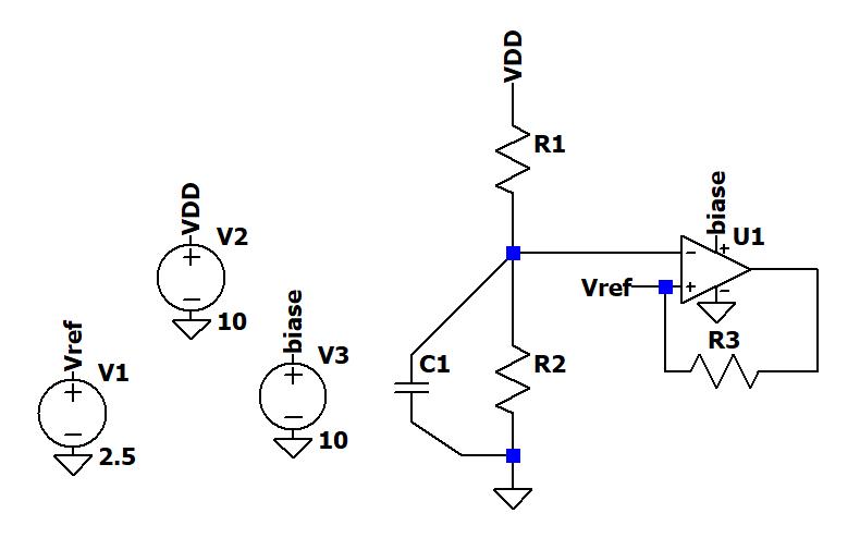
Theundervoltageisusedtoavoidthedamageofanydevicefromthevoltageratedbelowthespecification,in40WDC DC convertertheundervoltagerangeisbelow18vsothevoltagereachesbelow18Vthencurrentdrawingwillbemorefrom theinputsupplythiscausepowerloss,thenthevoltagesensingelementgetssensedandtheshutdownpinofPWMICgets high and converter gets turn off. the voltage should be of 125% of the rated primary voltage. By this we can avoid the damageofcomponentsintheconverter[2].
International Research Journal of Engineering and Technology(IRJET) e ISSN: 2395 0056
Volume: 09 Issue: 05 | May 2022 www.irjet.net p ISSN: 2395 0072
4.6.3
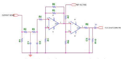
Fig 4: circuitofOverVoltageProtection
5:
Theovercurrentprotectionisusedtoavoidtheconverterfromthedamage.Ifthecurrentreachesabovethespecification, thenthecomponentsinconvertermaygetdamage.Sothevalueofthevoltagedividerresistorisdesignedaccordingtothe inputvoltagesupplyheretheinputvoltagerangeiffrom18 50VThecurrentlimitingresistorisdesignedaccordingtothe inputandoutputcurrent,whenthecurrentexceeds125%ofdesignedvalue.TheshutdownpinofPWMICgetshighand convertergetsturnoff[3].
International Research Journal of Engineering and Technology(IRJET) e ISSN: 2395 0056
Volume: 09 Issue: 05 | May 2022 www.irjet.net p ISSN: 2395 0072
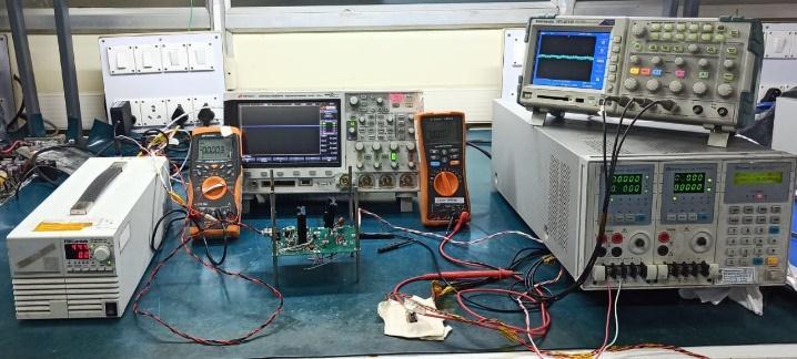
The output voltage is measured at the minimum to maximum input voltage and load conditions as we observe in the belowtable1.
Table 1: Output voltages at load from 10% 100% at input voltage of 18 50V
OUTPUT VOLTAGE(V)
VIN (V)
5V O/P (4.98 5.02) at 100% load 10% 50% 100% 18 5.010 5.011 5.012 28 5.010 5.011 5.011 50 5.010 5.010 5.011
Theinputcurrent,input power,andoutputpower,efficiencyof80% atminimumandmaximumisobservedin below table2.
Table 2. Efficiency at load from 10% 100% at input voltage of 18 50V
VIN (V)
Input current (A) Input power (W) Output power (W)
Efficiency(%) Spec:Min=75%, Nom=79%
10% 50% 100% 10% 50% 100% 10% 50% 100% 10% 50% 100% 18 0.364 1.400 2.784 6.55 25.20 50.11 4.01 20.04 40.10 61.2 79.5 80.0 28 0.269 0.913 1.785 7.53 25.56 49.98 4.01 20.04 40.09 53.2 78.4 80.2 50 0.202 0.558 1.045 10.10 27.90 52.25 4.01 20.04 40.09 39.7 71.8 76.7
5.3 Output ripple Voltage
Table 3. Output ripple voltages at load from 10% 100% at input voltage of 18 50V VIN (V)
OUTPUT RIPPLE VOLTAGE(mV)
5V O/P (V) Spec: Nom:20mV Max:50mV 10% 50% 100% 18 5 10.4 16.4 28 5.2 11.4 17.6 50 7.8 14.4 16.8
© 2022, IRJET | Impact Factor value: 7.529 | ISO 9001:2008 Certified Journal | Page3170
International Research Journal of Engineering and Technology(IRJET) e ISSN: 2395 0056
5.4 Line Regulation
5.5 Load Regulation
5.6 Inhibit
Table 4. Line regulation at load from 10% 100% Line regulation (mV) 5V Spec: ±10mV 10% 50% 100% Down Reg (mV) 0 0 1 Up Reg (mV) 0 1 0
Table 5. Load regulation at input voltage from 18 50V Vin (V)
Load regulation (mV) 5V 0.5%(25mV) +0.5%(25mV) 50% to 10% 50% to 100% 18 1 1 28 1 0 50 0 1
from
INHIBIT TEST Open Circuit voltage (3 5)V Voltage range ( 0.5 50)V Converter turn on voltage (> 0.8) V Drive current (sink) <(100uA) 18V (10% load) 3.98 0.5 to 50 1.36 18.4 18V (100% load) 4.11 0.5 to 50 1.39 21.23 50V (10% load) 3.99 0.5 to 50 1.26 49.97 50V (100% load) 4.34 0.5 to 50 1.25 49.97
5.7 Sync in/out
Parameter
Table 7. Sync test at frequency range from 450-600kHz
Volume: 09 Issue: 05 | May 2022 www.irjet.net p ISSN: 2395 0072 © 2022, IRJET | Impact Factor value: 7.529 | ISO 9001:2008 Certified Journal | Page3171
International Research Journal of Engineering and Technology(IRJET)
e ISSN: 2395 0056
Volume: 09 Issue: 05 | May 2022 www.irjet.net p ISSN: 2395 0072
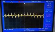
Therippleoutputwaveformof40WDC DCforwardconverterwithfullloadandmaximumvoltageisshowninthefig 7is havingtherippleof16.8mVandiswithinthespecification
Fig 7: InputVoltage=50V, CH4:5V/8A,Ripple:16.8mV
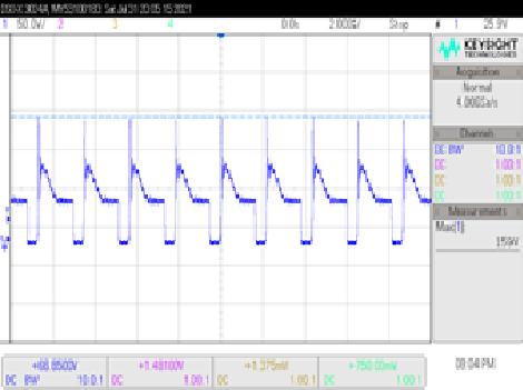
TheMOSFETdrainvoltageoutputwaveformof40WDC DCforwardconverterwithfullloadandmaximumvoltageis showninthefig 8ishavingthedrainvoltageof159Vandiswithinthespecification
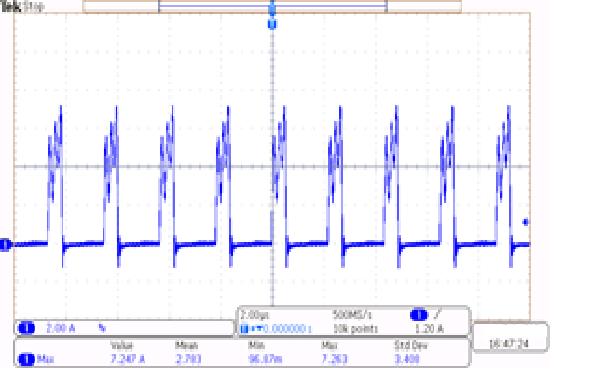
Fig - 8: Vin=50V,Max.DrainVoltage:159V
The MOSFET drain current output waveform of 40W DC DC forward converter with full load and maximum voltage is showninthefig 9ishavingthedraincurrentof7.247Aandiswithinthespecification.
Fig 9: Vin=50V,Max.Draincurrent:7.247A
© 2022, IRJET | Impact Factor value: 7.529 | ISO 9001:2008 Certified Journal | Page3172
5.11
International Research Journal of Engineering and Technology(IRJET) e ISSN: 2395 0056
Volume: 09 Issue: 05 | May 2022 www.irjet.net p ISSN: 2395 0072
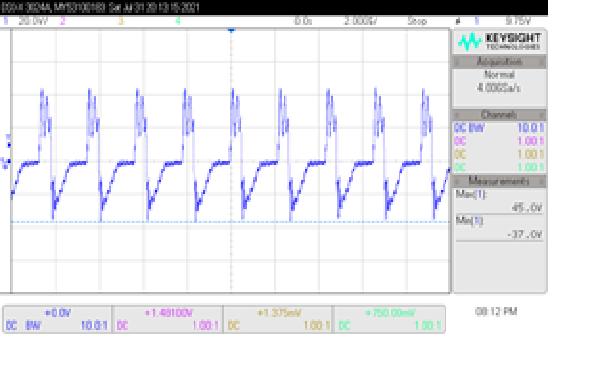
TheDiodestressoutputwaveformof40WDC DCforwardconverterwithfullloadandmaximumvoltageisshowninthe fig 10ishavingthediodestressofmaximumstressvoltageisbetween45V&37Vandiswithinthespecification.
Fig 10: Vin=50V,Max.StressVoltage:45V&37V
TheForwardconverterwithsingleoutputof5V/8Ahasbeensuccessfullyimplementedwithfeedforwardtechnique,sync in/out,andinhibitcircuits.Theoutputripple,MOSFETstress,Diodestress,Lineregulation,andLoadregulationiswithin thespecificationas observedinthepracticallyproved experimental resultsatthe full load100%and50%,10%withthe variableinputvoltage.The4 5%ofoverallconverterefficiencyisimprovedbyusingsnubbercircuit.Futureworkcanbe carriedoutonimprovingtheefficiencyanddigitallycontrolledMOSFET,feedforwardtechnology.
[1]S.Kuruva,C.G.Satyaraddi,K.E.Rayees,B.K.SinghandV.Chippalkatti,"DesignandImplementationofMultipleOutput DC DCConverterwithOutputPowerSequencing," 2021 6th International Conference for Convergence in Technology (I2CT), 2021,pp.1 7,doi:10.1109/I2CT51068.2021.9417822.
[2] Nagesh L., Bhanuprakash CV, B.K Singh, Vinod Chippalakatti. "Design and Implementation of Triple Output Forward DC DCConverterwithCoupledInductorasPost regulatorforSpaceApplication," 2020 International Conference on Smart Technologies in Computing, Electrical and Electronics (ICSTCEE), 2020, pp. 175 179, doi: 10.1109/ICSTCEE49637.2020.9276792.
[3] Chaitra G. Satyaraddi, A. Usha, Aravind Bhat, P.K. Praveen, Bhoopendra Kumar Singh, Vinod Chippalktti. "Design and Implementation of Multiple Output Interleaved Flyback Converter with Post Regulators," 2019 IEEE International Conference on Electrical, Computer and Communication Technologies (ICECCT), 2019, pp. 1 6, doi: 10.1109/ICECCT.2019.8869418.
[4] Sudeep E, Rachappa, B. K. Singh, V. S. Chippalkatti and K. U. Rao, "Design and implementation of current mode controlled 150W miniature forward converter for defence application," 2016 IEEE International Conference on Power Electronics, Drives and Energy Systems (PEDES),2016,pp.1 6,doi:10.1109/PEDES.2016.7914231.
[5] P. K. Rampelli, R. Deekshit, D. S. Reddy, B. K. Singh, V. Chippalkatti and T. Kanthimathinathan, "Multiple output magnetic feedback forward converter with discrete PWM for space application," 2012 IEEE International Conference on Power Electronics, Drives and Energy Systems (PEDES),2012,pp.1 6,doi:10.1109/PEDES.2012.6484471.
© 2022, IRJET | Impact Factor value: 7.529 | ISO 9001:2008 Certified Journal | Page3173