International Research Journal of Engineering and Technology (IRJET) e ISSN: 2395 0056
Volume: 09 Issue: 05 | May 2022 www.irjet.net p ISSN: 2395 0072
International Research Journal of Engineering and Technology (IRJET) e ISSN: 2395 0056
Volume: 09 Issue: 05 | May 2022 www.irjet.net p ISSN: 2395 0072
Pavan G1 , V Siddeswara Prasad2
1 Dept. Of E&IE, Siddaganga Institute of Technology (SIT), Tumkur, India. 2Professor, Dept. Of E&IE, Siddaganga Institute of Technology (SIT), Tumkur, India. ***
Abstract In today’s computer world, it is very necessary to improve the speed in most electronics devices. People are very much fascinated over new technologies. To fulfil the need of customers, it is a challenge to system designers when it comes to keeping up with speed. In choosing an optimal system, memory plays a vital role in the performance and reliabilityof system. Memory modules are important components of many very large scale integration (VLSI) designs. Presently in the market Double Data Rate 3rd Generation (DDR3) and Double Data Rate 4th Generation (DDR4) Synchronous Dynamic Random Access Memory (SDRAM) are often seen but their memory storage array implementation is not directly available to the user. The aim of the project is to develop a DDR4 memory model using system Verilog that fulfils the specifications of JEDEC Specs given by Solid State Technology Association. The memory model is built with improvisation in its efficiency in terms of data rate when compared to its previous generation. Since thepresentDDR4memory modelof different companies are confidential (encrypted format), user cannot access it directly. So, modellingofDDR4memory model helps the user to obtain the decrypted form of DDR4 memory model and helps in further upgradation according to requirements. The tools used for the project are Modelsim 6.3g p1 and Questasim. The implementation includes DDR4 memory modelling using the System Verilog, verification with Xilinx memory controller. Comprehensive simulations of all scenarios including bypass (Read Write of the same address, on the same cycle) will be performed followed by sequential equivalent checking versus an existing model using the Modelsim tools.
andassociatedprograms.Applicationsonsuchdeviceswill needlargeexternalRAM.Mostofthecontemporarydataisin the form of images, sound, real time signals, etc. which require very large memory to store and operate. Using GigabytesofRAMisnotveryuncommonincurrentprocessor scenario[1].
To facilitate system integrators to build such systems, standardizationofdeviceinterfacesisanecessity.Someof the standard memory interface technologies are SDRAM, RDRAM, DDR SDRAM, etc. There have been several advancements in DDR SDRAM technologies. The earliest SDRAMmoduleshadaclockfrequencyof133MHz[2].DDR doubled the transfer rate and worked at double the frequency,at266MHz.
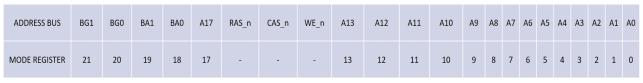
RecenttechnologiessupportDDRSDRAMrunningat1.6 GHz[2].Whilethelatestmemorytechnologiesareusedin high end processors, embedded systems rely on DDR2 runningat266MHz[3].DDRfamilyhasacommonhardware interface. So, it is easy to modify an existing interface hardwaretomatchanyothermemberoftheDDRfamilyas showninTable1.
Table -1: ComparisonofDDR4WithPreviousGeneration
Parameters DDR1 DDR2 DDR3 DDR4 Operating Voltage 2.5V 1.8V 1.5V 1.2V RAM Internal Clock Frequency (MHz)
Mostelectronicssystemsusememorycomponentseither for storing executable software or for storing data, and therefore the availability of accurate memory models is fundamental to most functional verification strategies. Makingthese modelsavailable inproven,standards based librariesisessential.DevelopmentsinVLSItechnologyare driven by the never ending demand for faster processors. Fasterprocessorsneedfastermemory.Onchipmemoryis built using the same technology as the processor but is limitedinsize[1].Manymicrocontrollershavefewkilobytes to few hundred kilo bytes of on chip RAM. However, this memory is hardly sufficient for resident operating system
266 400 533 800 1066 1600 2133 3200 Clock Frequency (MHz) 133 200 266 400 533 800 1066 1600
Bitsper cycle 2 4 8 8
ThemainaimoftheprojectistobuildaDDR4Memory ModelusingsystemVerilogtoimprovetheefficiencyinterms ofdataratewhencomparedtoitspreviousgeneration.Since the present DDR4 is of encrypted form, which cannot be altered by a user according to their requirements. So, the main objective is to decrypt the DDR4 with reference to DDR3accordingtotheJEDECSpecofDDR4withthehelpof software tool Modelsim which helps to design a fastest
2022, IRJET | Impact Factor value: 7.529 | ISO 9001:2008 Certified Journal

International Research Journal of Engineering and Technology (IRJET) e ISSN: 2395 0056
Volume: 09 Issue: 05 | May 2022 www.irjet.net p ISSN: 2395 0072
memorymodelwithhighspeedandlesspowerconsumption. VerificationofDDR4memorymodelincludescomparisonof data rate in terms of delay with respect to its previous generationDDRSDRAM.
Large scale research is being done in the field of memory technologytoincreasetheefficiencyofmemorymodelling. Thisefforthasnotalwaysbeensuccessfulbecause,during the fabrication process, the densely packed memory structures can experience defects. Therefore, it is not suitabletotestthememorymodulesoncetheyarepacked. Functionalverificationofamodulealongwithtesting,makes surethatthedesignworksthewayithasbeendesignedto perform.
Manikandan Sriram and Mohan Dass have briefly explainedtheoryofthememorymodelin[2].Alayeredtest bench has been designed using Universal Verification Methodology(UVM),astandardizedclasslibrary,whichhas increased the reusability and automation of the existing designverificationlanguage,SystemVerilog[2].
Prajakta Chandilkar and Dr. Uday Wali have explained about the implementation of finite state machine(FSM)of DDR2SDRAMmodule[1].
DDR2 model can be referred to as the basic model for hardwaredesignofotherupgradedmemorymodules.The basic operations such as READ WRITE, and a high level picture of SDRAM sub systems, is very necessary to understand the basic concept of DDR4 memory model physicalstructure[1].
in
LengthOf4
followedbyareadorWritecommand.Thereadoperation startswithanaddresscorrespondingtoA2,A1,A0asshown inTable2.Theaddressbitsregisteredcoincidentwiththe Read or Write command are used to select the starting columnlocationfortheburstoperation,determineiftheauto pre chargecommandistobeissued(viaA10),andselectBC4 orBL8modeifenabledinthemoderegister.Priortonormal operation, the DDR3 SDRAM must be powered up and initializedinapredefinedmanner.
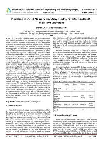
BlockdiagramofthecompletesystemisshowninFigure1 and the pin diagram of DDR4 memory model is given in Figure6.
8
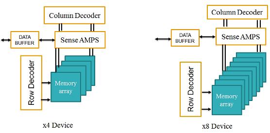
DDR4 functional diagram consists of Control logic which controls the overall operations of DDR4, where the Mode RegisterSet(MRS)commandisusedtoupdatethecontrol registers. Control registers are used to store parameters relatedtocommunicationprotocol,addressmode,refresh rate,commandpipeline,databufferingetc.Herethestorage elementsarememorybankarrays,thatconsistsofmultiple numbersofrowsandcolumns.DDR4consistsoffourbanks i.e., two banks per bank group as shown in Figure 2. On power up, the ZQ calibration is initialized through ZQCL command as shown in Figure 3. At the same time DQ calibrationcontrolblockisenabledtoresettheDRAMvalues asshowninFigure4.ModeRegisterscanbeprogrammed accordingtotheoperationstobeperformedonthememory model. The pin mapping in the MRS is given in Figure 5 where the RAS n, CAS n, WE n controls the different operationsaccordingtothefunctionaltableshowninTable 3.OperationsbeginswiththeActivecommandwhichisused toselectthebankandrowtobeaccessed,whereBA[1:0] select the bank, and A [17:0] select the row by using Row and Column decoder. MRS programming is done after RESET,whichisthenfollowedbyWRITEorREADcommand, after read/write pre charge command should be issued whichensuresthatthedataiswrittenorreadinamemory.
The few scenarios to be checked in any DRAM during operationare:
1.WriteandReadtomemorylocation:Performwriteto anymemorylocation,readfromthesamememorylocation, readdatashouldbesameaswrittendata.
2.WriteandReadtoallmemorylocation:Performwrite andreadoperationtoallthememorylocations.
DDR3 SDRAM is internally configured as an eight bank DRAM. To achieve high speed operation, it uses an 8n prefetcharchitectureto.Asinglereadorwriteoperationfor theDDR3SDRAMconsistsofasingle8n bitwide,fourclock data transfer at the internal DRAM core and eight correspondingn bitwide,one halfclockcycledatatransfers attheI/Opins.ReadandwriteoperationtotheDDR3SDRAM areburstoriented:startattheselectedlocationwithrespect towriteoperationandcontinueforaburstlengthofeightor a chopped burst of four in a programmed sequence. Operation begins with an Active command, which is then
3. Default memory value check: Before writing any locationscheckthedefaultmemoryvalue,doreadoperation togetdefaultvaluesashFF.
4.ResetinMiddleofWriteorReadOperation:Applyreset in between write or read operation and check for default values present in memory. (After writing to few locations apply the reset and perform read operation, to get default memorylocationvaluehFF.
2022, IRJET | Impact Factor value: 7.529 | ISO 9001:2008 Certified Journal |
International Research Journal of Engineering and Technology (IRJET) e ISSN: 2395 0056
Volume: 09 Issue: 05 | May 2022 www.irjet.net p ISSN: 2395 0072
ZQCalibrationisrelatedtothedatapins[DQ]whereDQpin is bidirectional. When a ZQCL command is issued during initialization,theDQcalibrationcontrolblockisenabledand an internal comparator within the DQ calibration control blocktunesthep channeldevicesusingVOH[0:4]untilthe voltageisexactlyVDDq/2.Atthispointthecalibrationhas beencompleteandtheVOHvaluesaretransferredtoallthe DQpins.
Fig 1:FunctionalBlockDiagramofDDR4.
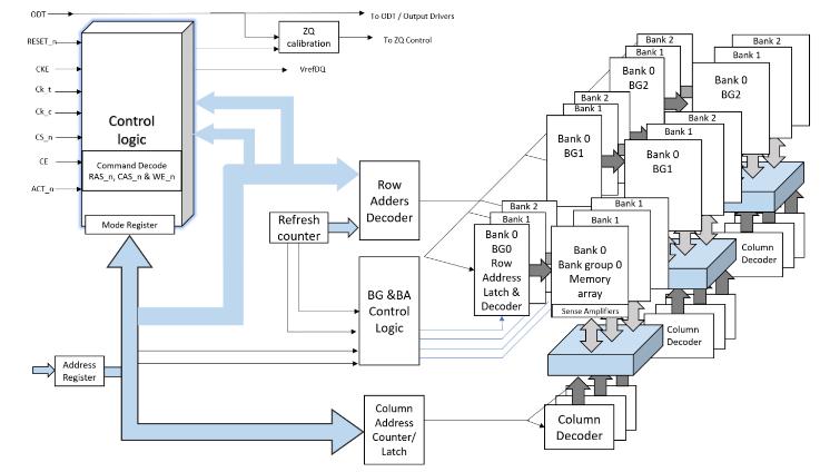
Memory bank is a logical storage unit of memory which containstheaddressprovidedbytheuser,wherethislogical addressisconvertedtoaphysicaladdressbeforeitisgiven toDRAM.ThephysicaladdressismadeupofBank Group, Bank,Row,Column where thesizeofthe memory bank is determined by bits in a column and rows. Row column organizationofthebankisconfiguredusingMRScommands. DRAMs are classified as x4 to x16 based on this column width as shown in Figure 2. The width of DQ data bus is sameasthecolumnwidth.So,DRAMsareclassifiedbasedon thewidthoftheDQbus.
Fig 2:MemoryBankArray.
Databufferisusedtotemporarilystorethedata,whileitis moving between controller and the memory. DQ is a bidirectionaldatabuswhichcanbeusedtoreadadatafrom agivenaddresslocationorwriteadatatoagivenaddress location.
Fig 3:ZQCalibration
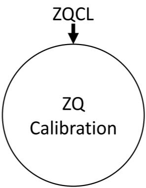
Fig 4:DQCalibration.
Forapplicationflexibility,variousfunctions,features,and modes are programmable in seven mode registers (MRn) providedbythedeviceasuserdefinedvariablesthatmustbe programmedvia aMODEREGISTER SET(MRS)command. Because thedefault values of the mode registers are not defined,contentsofmoderegistersmustbefullyinitialized and/or re initialized; that is, they must be written after power upand/orresetforproperoperation.Thecontentsof themoderegisterscanbealteredbyre executingtheMRS commandduringnormaloperation.Whenprogrammingthe moderegisters,eveniftheuserchoosestomodifyonlyasub setoftheMRSfields,alladdressfieldswithintheaccessed moderegistermustberedefinedwhentheMRScommandis issued.
International Research Journal of Engineering and Technology (IRJET) e ISSN: 2395 0056
Volume: 09 Issue: 05 | May 2022 www.irjet.net p ISSN: 2395 0072
Fig 5:Addresspinmapping.
PinconfigurationisshowninFigure6andeachpincarryits ownfunctionality;thefunctionsareasfollows:
Clock (CKt CKc): CKt andCKc are differential clock inputs, where all address and control inputsignals aresampledatthepositiveedgeofCKtandnegative edgeofCKc.
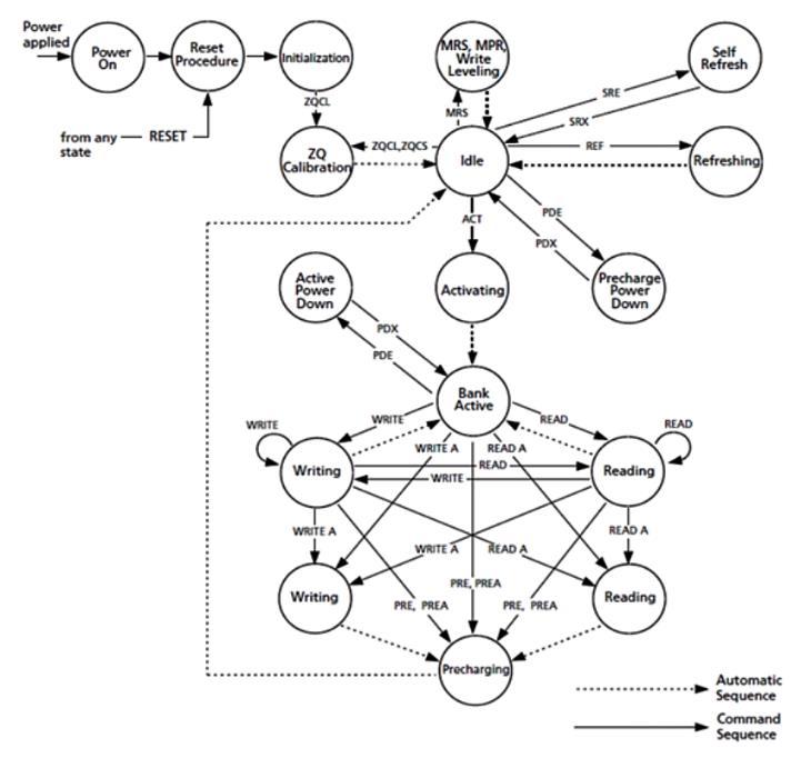
State diagram describes the state transition diagram for DDR4SDRAM.Thereare10states.TheyareInitialization, Idle, Refresh, MRS, Active, Writing, Reading, Pre charge. commandsetstobeissuedincludesRES,REF,ACT,WRITE, READ, PRE and NOP. The different operations can be performedonDDR4 byalteringRAS bar,CASbar,WE bar respectivelyasshowninTable3.
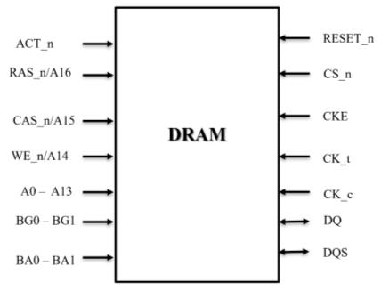
Table 3: FunctionalTableforDDR4SDRAM
Command RASbar CASbar WEbar
ClockEnable(CKE):Itactivatesalltheinputsignals. ChipSelect(CSn):All commandsaremaskedwhen CSnisregisteredHIGH.
Activation Command Input (ACTn): Activation command being entered along with CSn, which activatestheDRAM.
CommandInputs(RASn/A16.CASn/A15.WEn/A14): RASn/A16, CASn/A15 and WEn/A14 define the command being entered for different memory operations.Thosepinshavemulti function.
BankGroupInputs(BG0 BG1):BG0 BG1defineto which bank group an Active, Read, Write or Pre charge command is being applied. BG0 also determines which mode register is to be accessed duringanMRScycle.
NOP/Idle H H H Read H L H Write H L L Pre charge L H H Refresh L L H MRS L L L
AddressInputs(A0 A17):Providetherowaddress forACTIVATECommandsandthecolumnaddressfor ReadorWritecommandstoselectonelocationoutof thememoryarrayintherespectivebank.
ActiveLowAsynchronousReset(RESETn):Resetis an active LOW pin which is active during normal operation when it is LOW, and inactive when it is HIGH.
Toensureproperdevicefunction,thepower upandreset initializationdefaultvaluesforthefollowingMRsettings aredefinedas:
Gear downmode(MR3A[3]):0=1/2rate
Per DRAMaddressability(MR3A[4]):0=disable
DataStrobeinput/Output(DQS):TheDatastrobeis essentially a data valid flag. Read data are edge aligned,writedataarecanteredaligned.
Maximum power saving mode (MR4 A [1]): 0 = disable
CStocommand/addresslatency(MR4A[8:6]):000= disable
CAparitylatencymode(MR5A[2:0]):000=disable
Hard post package repair mode (MR4 A [13]): 0 = disable
Fig 6:DDR4memorymodelpindiagram.
2022, IRJET | Impact Factor value: 7.529 | ISO 9001:2008 Certified Journal
International Research Journal of Engineering and Technology (IRJET) e ISSN: 2395 0056
Volume: 09 Issue: 05 | May 2022 www.irjet.net p ISSN: 2395 0072
Fig 7: StatetransitiondiagramforDDR4SDRAM.
Thefollowingsequenceisrequiredforpower upand initialization:
1.Applypower.RESETnmustremainbelow0.2VDDfora minimumof700swhensupplieshaverampeduptoavalid stable level. CKE is pulled LOW whenever RESETn is de affirmed(minimum10nstime).Theramptimeofthepower voltagefrom300mVtoVDD,VDDmustbegreaterthanor equal to VDDQ and 0.3 (VDD VDDQ). VPP must be always equaltoorhigherthanVDD.AftertheVDDwentoff.RESETn must go high within 10 minutes of VDD ramping up to a stable level. After RESETn goes high, the initialization sequencemustbestartedwithin3seconds.
2.Waitforanother500sbutnolonger3secondsuntilCKE becomesactiveafterRESETnisde affirmed.Thedevicewill initialize internal state during this time; this will be done regardlessofexternalclocks.
3.BeforeCKEbecomesactive,clocks(CKt,CKc)mustbe startedandstabilizedforatleast10nsor5tCK(whicheveris bigger).SinceCKEisasynchronoussignal,theappropriate setuptimemustbemettoclock(tIS).ADESELECTcommand mustalsoberecordedattheedgeoftheclock.
4.WaitaminimumofRESETCKEEXITtimebeforeissuing thefirstMRScommandtoloadthemoderegisterafterCKEis registeredHIGH(tXPR=MAX(tXS,5tCK).
5.IssueMRScommandtoloadMR3,MR6,MR5,MR4,MR2 andMR1withallapplicationsettings,waittMRD.
6.IssueMRScommandtoloadMR0withallapplication settings,waittMOD.
7.IssueaZQCLcommandtostartZQcalibration.
8.WaitfortDLLKandtZQinittocomplete.
OncetheDRAMhasbeeninitialized,iftheDRAMisinidle statelongerthan960ms,either(a)REFcommandsmustbe issuedwithintREFIconstraints(postingpermitspecification) or(b)CKEorCSnmustswitchoncewithineach960msidle timeinterval.Onpowerup,theDDR4moduleisintheIdle state which means no operation is being performed or scheduled. It is generally during such periods that auto refresh works in the background to keep the memory contentsstable.Onpowerup,pre chargecommandisapplied to the memory module. If pre charge command is issued during normal usage, open row of the active bank is deactivated, and the new bank is activated. Therefore, the data before andafter the pre charge command will notbe consistent. Once all banks are pre charged, the memory moduleentersidlestate.ThenanMRScommandshouldbe issued to enable different control signal of DDR4, e.g., DLL reset, burst length, and burst Mode etc. Next a Refresh commandshouldbeissued.Thiscommandisusedtorefresh data in selected bank. This command opens a specific memoryarray bank. Youcan reador writethe memoryat this point. Initially, before reading, memory should be written.Butthisisnottrueforothermemorytypes,suchas flashRAM.Todeactivatethecurrentopenbankandreturn the device to idle state, pre charge command should be issuedattheend.
DesigningofDDR4isdonebySystemVerilog,theoperations onDDR4isanalyzedusingModelsim6.3g p1andQuestasim.
ModelSim is Mentor Graphics’ multi language HDL simulationenvironmentforsimulatinghardwaredescription languageslikeVHDL,VerilogandSystemC,andincludesan integrated C debugger. In conjunction with Intel Quartus Prime, Xilinx ISE or Xilinx Vivado, ModelSim can be used independently. Using the graphical user interface (GUI), simulationcanbedone.
ModelSimincreasesdesignqualityanddebugproductivityin addition to supporting standard HDLs. ModelSims technology allows VHDL and Verilog to be transparently mixed in one design. Its architecture enables platform independentcompilationwithoutstandingnativecompiled codeperformance.
Using Modelsim, DDR3 memory model is analyzed by considering the standard timing parameters provided by micron technologies. The commands used to simulate the memorymodelare:
International Research Journal of Engineering and Technology (IRJET) e ISSN: 2395 0056
1. Vlibwork
2. Vlog sv+define+sg125 +define+den4096Mb ddr3.sv ddr3 module.vtb.v
3. Vsimwork.tb
4. Addwave r/*
5. run all
once the waveforms are obtained, the delay between differentoperationsaretabulatedintheTable4intheresult section.
The Questa Advanced Simulator is Questa Verification Solution’s core simulation and debug engine; the comprehensiveadvancedverificationplatformthatreduces the risk of validating complex FPGA designs. The Questa AdvancedSimulatoristhecoresimulationanddebugengine of the Questa Verification Solution; the comprehensive advancedverificationplatformcapableofreducingtherisk ofvalidatingcomplexFPGAdesigns.
Using this platform, DDR4 memory model is designed accordingtotherequiredspecificationsgivenbyJDECspec standards. Using Modelsim, DDR4 memory model is analyzed by considering the standard timing parameters provided by micron technologies. The commands used to simulatethememorymodelare:
1.vlibwork
2.vlog workwork+acc lvcs.log novopt sv+define+DDR4 8G X8arch package.sv
3. proj package.sv interface.sv StateTable.svp MemoryArray.svpddr4 model.svptb.sv
4.vsim novopttb
5.run all
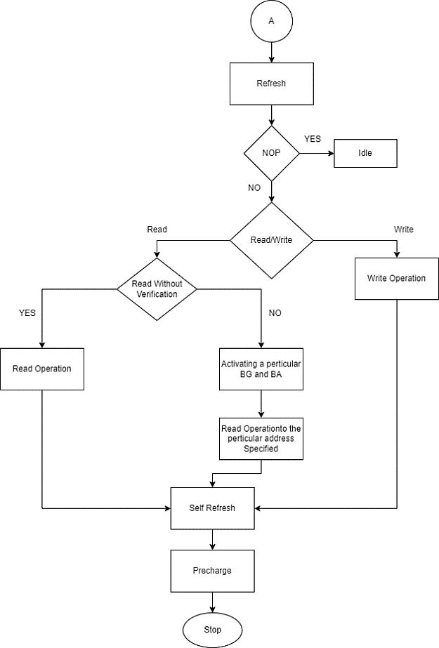
once the waveforms are obtained, the delay between differentoperationsaretabulatedintheTable4underresult section.Figure8representstheflowofDDR4memorymodel withrespecttoStateTransitiondiagramshowninFigure7, wherethedifferenttasksaredefined.
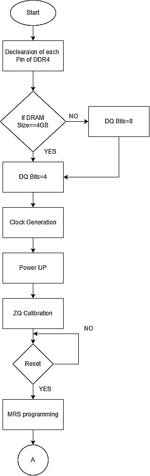
Fig-8:FlowChartofDDR4MemoryModel
Volume: 09 Issue: 05 | May 2022 www.irjet.net p ISSN: 2395 0072 © 2022, IRJET | Impact Factor value: 7.529 | ISO 9001:2008 Certified Journal
International Research Journal of Engineering and Technology (IRJET)
e ISSN: 2395 0056
Volume: 09 Issue: 05 | May 2022 www.irjet.net p ISSN: 2395 0072
The DDR4 memory model is designed and successfully simulated using Modelsim and Questasim, where the differentoperationsaresimulatedthatisIdle,Reset,Refresh, MRS,Active,Write,Read,Pre chargeetc.
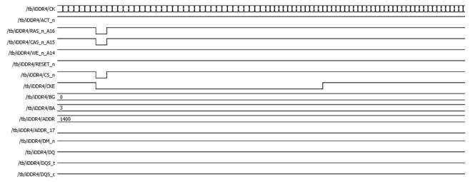
InitiallyDDR4isinidlestatewithrandomBankGroupand BandAddressselectedwith(RASn,CASn,WEn)=(1,1,1) withResetactiveandClockEnableZero(CKE=0)asshown inFigure9.
ToensuredatastoredintheSDRAMisnotlost,thememory controllermustissueaREFRESHcommandforanaverage intervaloftREFI.ButbeforeREFRESHisapplied,allbanksof the SDRAM must be pre charged and idle for a minimum timeoftRP(min).OnceaREFRESHcommandisissued,there must be a delay of tRFC (min) before the next valid commandisissuedasshowninFigure12.
Fig 9:IDLEstate(RASn=1,CASn=1andWEn=1)
TheDDR4isresetwithChipselectzero(CSn=0)andclock enablezero(CKE=0)asshowninFigure10.
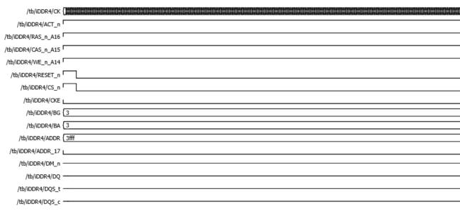
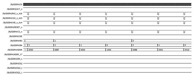
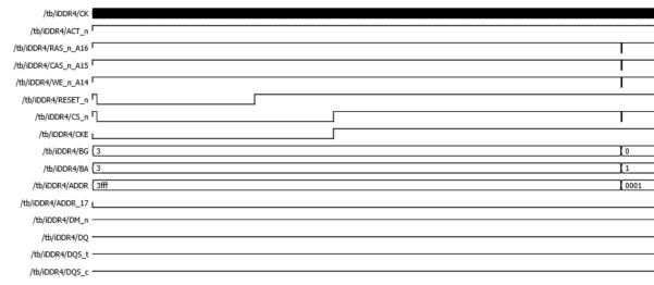
Fig 12:RefreshOperation(RASn=0,CASn=0and WEn=1).
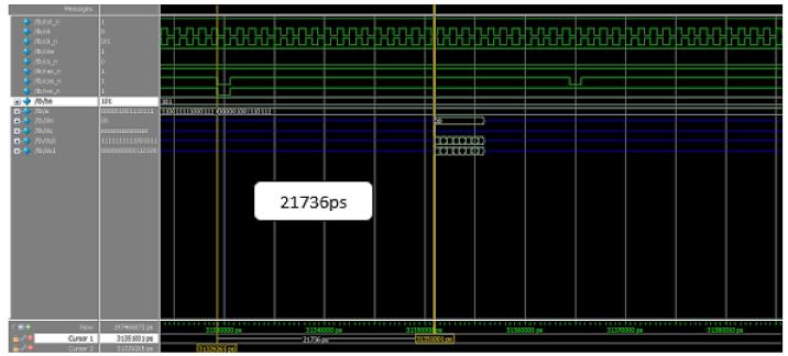
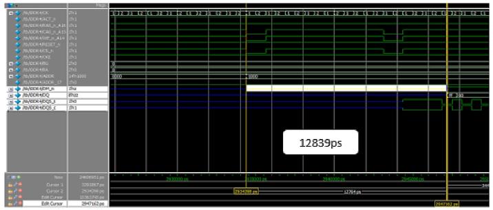
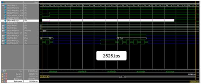
BeforewritingonDDR4memorymodel,Resetthememory andthenprovidewritecommandby(RASn,CASn,WEn)= (1,0,0)withaminimumdelaytowriteonDDR4memory. Erroroccursifminimumdelayisnotconsidered between twoconsecutivecommandswheredelaysarecalculatedand comparedbetweenDDR3andDDR4showninFigure13and 14respectively.
Programming7MRSofDDR4with(RASn,CASn,WEn)=(0, 0,0)with7differentaddressesbyselectingBankGroupand BankAddress.SDRAMsprovideseveralfeatures,functions and settings which can be programmed using the 7 Mode Registers.TheseregisterscanbeprogrammedusingtheMRS command.TheModeRegistersaresetduringinitialization and thereafter they can be changed at any time during normaloperationshowninFigure11.
13: DelaybeforeWriteOperationinDDR3.
Fig 14: DelaybeforeWriteOperationinDDR4
Fig 11: MRSProgramming
International Research Journal of Engineering and Technology (IRJET) e ISSN: 2395 0056
Volume: 09 Issue: 05 | May 2022 www.irjet.net p ISSN: 2395 0072
Fig 15:WritingadatatoaMemory
Data (00,ff,00)onBG=0,BA=0of(Address=0000).When DQS t and DQS c toggles the data is written on DDR4 memoryshowninFigure15.
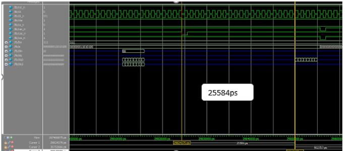
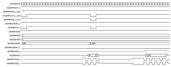
Read command by (RASn, CASn, WEn) = (1, 0, 1) with a minimum delay to read data from DDR4 memory where delayiscalculatedandcomparedbetweenDDR3andDDR4 asshowninFigure16and17.DatastoredinBG=’0’,BA=’0’, Address=’0000’ can be read from DDR4 memory error occurs if minimum delay is not considered between two consecutivecommandsasshowninFigure18.
Fig-18:ReadingadatafromaMemory
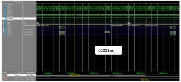
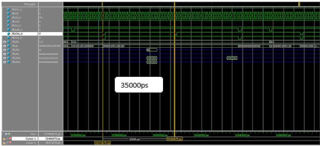
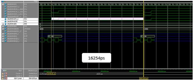
Thereshouldbesomedelaybetweenanytwoconsecutive operationsinaMemorymodel,wherethedelayiscalculated andcomparedbetweenwriteandreadoperationinDDR3 andDDR4whichisshowninFigure19and20respectively. ThedelaybetweenreadandwriteoperationinDDR3and DDR4 are calculated as shown in Figure 21 and 22 respectively
Fig 19:Minimumtimebetweenwriteandread operationinDDR3.
Fig 16:Delaybetweenreadcommandtodataoutin DDR3
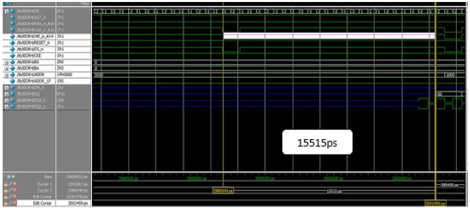
Fig 20:Minimumtimebetweenwriteandread operationinDDR4
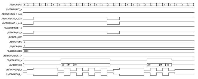
Fig 17:Delaybetweenreadcommandtodataoutin DDR4.
Fig-21:Minimumtimebetweenreadandwrite operationinDDR3
International Research Journal of Engineering and Technology (IRJET) e ISSN: 2395 0056
Volume: 09 Issue: 05 | May 2022 www.irjet.net p ISSN: 2395 0072
Fig 22:Minimumtimebetweenreadandwrite operationinDDR4
Pre chargemustbedoneifdifferentBGneedtobeselected i.e.,Pre chargecommandby(RASn,CASn,WEn)=(0,1,0). Sincedataisstoredinsenseamplifierduringwriteorread command,itmustbesenttomemoryfromsenseamplifier during write command or read from memory to sense amplifierduringreadcommandasshowninFigure23.
Modelling of DDR4 memory and advanced verification of DDR4Subsystemisfocusedondesigningandimplementing the DDR4 memory according to DDR4 SDRAM JEDEC specifications,wherethereadandwriteoperationsofDDr4 is compared and tabulated with respect to DDR3. The designedDDR4consumeslesserpowerandhasgreaterdata transferratecomparedtoitspredecessori.e.,DDR3,DDR2 and DDR. Its application ranges from low power mobile computingdevicetohighdensityservers.Sincethereisan aggressive competition between different companies, the companiesprefertokeeptheirresearchfindingconfidential, hence the upgradation of models becomes difficult. Therefore, the designed DDR4 model enables for easy upgradation.
[1] PrajaktaChandilkarandDr.UdayWali,“Developmentof DDR2 SDRAM Module Interface Software Core”, International Journal of Engineering Research and Application,pp.28 32,September2017.
[2] Manikandan Sriram Mohan Dass, “Design and Verification of a Dual Port RAM Using UVM Methodology”, IEEE Transactions on Memory management, volume 14, no.5, pp.1217 1243, June 2018.
Fig-23:PRECHARGEOperation(RASn=0,CASn=1and WEn=1)
Byconsideringtheresultsobtained,thecomparisonofDDR3 and DDR4 is done by comparing the time delay between write/read command to the operation performed, and between any two operation that is either write to read or readtowritewhichisshowninTable4andTotaltimetaken toreadandwritethedatatoamemoryaddressiscalculated.
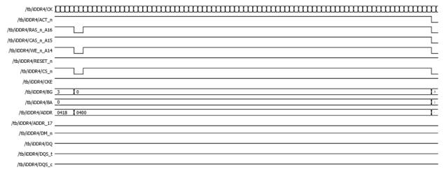
Table 4: ComparisonofDDR3andDDR4DuringReadand WriteOperation Operations DDR3(ps) DDR4(ps)
Writecommandto datawritten 21736 12839
Readcommandto dataread 25584 15515
Writeandread 35000 26261
Readandwrite 61029 16254
Writeoperation 6250 4978
Readoperation 7059 5643
By taking table into consideration, it can be said that the delay calculated in DDR4 is less than a delay occurred in DDR3.Hence,the performanceof DDR4memorymodel is enhancedintermsofdatarate.
[3] Md.AshrafulIslam,Md.YeasinArafath,Md.JahidHasan, “DesignofDDR4SDRAMController”,8thInternational ConferenceonElectricalandComputerEngineering,20 22December2014.
[4] JEDECStandard,“DDR3SDRAMSpecifications”,JESD86 3B,JEDECSolidStateTechnologyAssociation,January 2009.
[5] JEDECStandard,“DDR2SDRAMSpecifications”,JESD79 2B,JEDECSolidStateTechnologyAssociation,January 2005.
[6] “URL:https://www.systemverilog.io/ddr4 basics”.
[7] “URL:https://www.micron.com/ edia/client/global/documents/products/datasheet/dra m/”
2022, IRJET | Impact Factor value: 7.529 | ISO 9001:2008 Certified Journal