International Research Journal of Engineering and Technology (IRJET)

Volume: 09 Issue: 04 | Apr 2022
e ISSN: 2395 0056
p ISSN: 2395 0072
International Research Journal of Engineering and Technology (IRJET)
Volume: 09 Issue: 04 | Apr 2022
e ISSN: 2395 0056
p ISSN: 2395 0072
Shikha Goswami
, Dr. Satnam Singh2
1Research Scholar, Department of Electronics & Communication Engg P.K University, Shivpuri M.P, India
2 H.O.D Electronics & Communication Engg. Deptt, P.KUniversity, Shivpuri M.P, India
Abstract - Lately interests have been found in remote framework andprogrammingradioutilizingsigma-delta modulators to digitize signals close to the front finish of radio recipients. Such applications require timing the modulators at a high recurrence (MHz or above). A constant time execution utilizing trans-guides and integrators asopposedtodiscretetimeexecutionutilizing exchangedcapacitors is likedforhighrecurrenceactivity. An original cross coupled functional trans-conductance speaker (OTA) has been created with high linearity at high recurrence which can be utilized in plan of nonstop time sigma delta modulator. The proposed cross coupled OTA accomplishes gain of 35dB, third request Intermodulation (IM3) of - 73dB at a high recurrence scope of 70 MHz with a powerful Transconductance of 3.34mA/V. TheproposedOTAis executedin 180nmCMOS innovation
Keywords Analog and Mixed Signal IC Design, OTA, Linearization, Source Degeneration and Cross Coupling
Channels are to be carried out utilizing an OTA C geography.Consequentlytheprimarypieceofthemodulator istheOTA.Theguidelinesubtletiesofcirclechannelarehigh linearity, high tuneablility and high DC gain [1]. The base commitment of the modulator is directed by the data suggested uproar seen at the trans guide, and the most outrageousinformationisconfinedbythelinearityoftrans guide, since semiconductors have nonlinear lead at high repeatandpresentconsonantturns[2].Forthemostpart, the one of a kind extent of all around modulator is constrained by the data trans guide. The bending of the othertransconductorintheplanstreamwillmakeinband commotionandadditionallydegeneratetheSNDRandDRof modulator [3]. Accordingly, the transconductor should be altogetherstraight.Theturningoftheothertransconductor inthearrangementstreamwilldeliverinbanduproarand besides degrade the SNDR and DR of modulator [3]. Henceforth, the transconductor ought to be significantly straight.
***
DC gain 35dB Gm 3.34mA/V IM3at70MHz 73dB
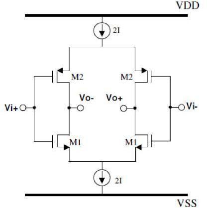
Thispaperwillfocusinonthearrangementoffunctional transconductanceenhancer(OTA).Theintroductionofthe sigma delta modulatorisaddressedbythecircle.Theease and linearity are the crucial features of the OTA made arrangements for any application. Colossal transconductancesareexpectedforthebandpassresonator working at 70 MHz, and their execution by and large uses hugeestimationsemiconductorsandtail current.Notwith standing,semiconductorswithgiganticsizepresentparasitic posts at lower frequencies. The usage of tremendous tail currentwillsimilarlygrowthepoweruseandfurtherreduce theDCgainofsemiconductors[4].Ageneraldifferentialpair hasarespectablerepeatresponseasaresultofthedeficitof low repeat parasitic posts. The issue of this topography is that the DC procure is incredibly confined. Cascode yield stagescanhelptheprocureanywaypresentparasiticshafts at the cascode center. A useful OTA subject to the indispensabledifferentialsetswasrepresentedin[9],andis shownFigure2.WhendifferentiatedandactivityampsOTA's are a ton faster and doesn't encounter the evil impacts of bandwidth and slew rate requirements.There are various kinds of linearity methodologies like source degeneration usingresistors,crosscouplingstrategiesaccordinglyon.This paperunitesboththetechniquestofurtherdeveloplinearity andgainofthefunctionaltransconductancespeaker.
International
Journal of Engineering and Technology (IRJET)
Volume: 09 Issue: 04 | Apr 2022
e ISSN: 2395 0056
p ISSN: 2395 0072
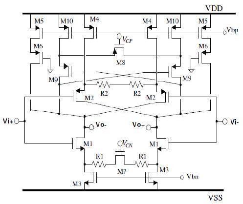
The OTA uses two differential sets M1 and M2 as the driving stage, and both differential sets draw from a comparative tail current. The fruitful transconductance increasesyetthepoweruseisn'textended.Onepieceofthe differentialyieldcurrentcomesfromN typesetsM1,andthe other from P type sets M2. With the help of minimal sign semiconductormodel,thefruitfulOTAtransconductanceis givenby,
Gm=gm1+gm2 (1)
Wheregm1andgm2areminimalsigntransconductances ofM1andM2,independently.Thereareacoupleofcircuit techniquesdefinitewithfurtherdevelopedlinearityofMOS transconductors. Most normally used linearization procedures are nonlinear term dropping, debilitating and sourcedegeneration[1].Nonlineartermfixingisrecognized by techniques for ideal arithmetical measure of nonlinear term.Inanycasetheimmediatereachisincrediblyrestricted and a fair clearing out is hard to achieve [10]. In the decreasingmethod,thedatavoltageisreducedortightened byacoupleoffactorsindegreetoworkonthelinearity.The disadvantage is that a higher expansion is expected to compensatethedatareducing,achievinggiganticzoneand more power usage. Stood out from the two techniques, sourcedegenerationisastrategybyandlargeused.
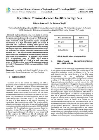
Thedifferencebetweenthetwodevelopmentsishowthe ongoingsourceisrelated.Plan2(a)hashighertypicalmode voltageswingatinput.Inlikemannerthefusscontributed bycurrentsourceismixedtoasingularyieldandseemslike differential uproar at the yield center point. In structure 2(b),theracketgoesthroughthetwobranchessimilarly,and seemslikeordinarymodeupheaval.
The proposed cross coupled OTA combines the two techniques uncovered in [4], [3] and [2].[4] uses source declinedOTAandhasIM3of 62dB,dcincrementof14dB and Unity secure repeat of 4.7GHz and is showed up underneathinfigures2.3,2.4and2.5.Insolicitationtosurvey the expansion of OTA using source degeneration[4] AC assessmentisactedincadencetogetgain.PSSexaminationis performed by applying two tone signal preliminary of 70MHzand71MHztogetIntermodulationproduct(IM3).
International Research Journal of Engineering and Technology (IRJET)
Volume: 09 Issue: 04 | Apr 2022 www.irjet.net
e ISSN: 2395 0056
p ISSN: 2395 0072
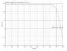
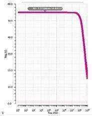
Figure 4.2: Response of AC analysis showing gain and UGB
Figure 4.5: Complete OTA structure
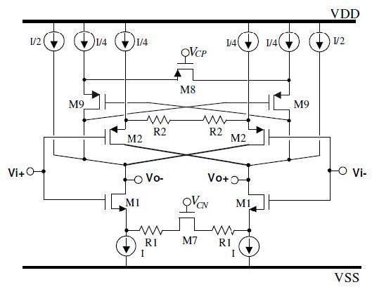
TheproposedOTAisshownbelow.sourcedegeneration and cross couple cancellation are employed to achieve a highlinearity
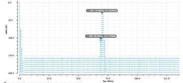

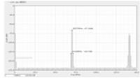
Figure 4.6: Schematic of proposed OTA
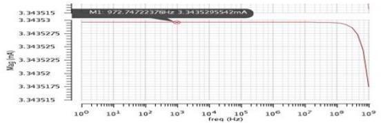
Figure 4.7: PSS analysis to calculate IM3
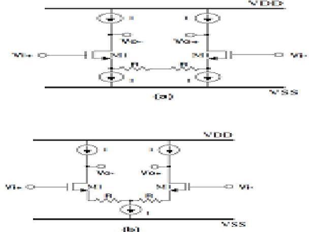
Figure 4.4: Proposed OTA
CurrentsourcesarecompletedbysemiconductorM3,M4 and M5. The components of M5 (M6) are on various occasionsthesizeofM4(M2)togiveM2thepropertendency current and reduce the fumble. A power supply of1.8 V is usedsothereissomeheadroomforthedevelopment.Poly resistors, as opposed to semiconductors, are used to do sourcedegenerationresistorsbecauseoflittleblockandthe nonlinearityofdynamicparts.
© 2022, IRJET | Impact Factor value: 7.529 | ISO 9001:2008
Figure 4.8: Proposed OTA
|
4025
International Research Journal of Engineering and Technology (IRJET)
Volume: 09 Issue: 04 | Apr 2022 www.irjet.net
ThePerformanceComparisonofsourceweakenedOTA[4] andProposedOTAisshowedupintable2.Itwillingeneral beseenthattheexpansionhasextendedby19dBandIM3is almost same.UGB of proposed OTA has diminished to 1.2GHz.TheproposedOTAcanbeusedinthearrangement ofrelentlesstimecirclechannelwhichistheprimarysquare ofsigmadeltamodulator
This research was supported by P.K University. We are thankful to our colleagues who provided expertise that greatlyassistedtheresearch,althoughtheymaynotagree withalloftheinterpretationsprovidedinthispaper.
Wearealsogratefulto Dr.Satnamsinghsirforassistance withlinearizationtechnique alsowhohad moderatedthis paperwithtechnicalmanuscript.
Iwouldalsoliketothankmyfamilyforsupportingmefor everything, and especially I can’t thank you enough for encouragingmethroughoutthisexperience.
© 2022, IRJET
e ISSN: 2395 0056
p ISSN: 2395 0072
[1] J.silva MartinezandE.sanchez,”CMOStransconductance amplifiers,architectures and filters:a tutorial”,in IEEE proceedings on circuits devices,vol.147, pp 3 12, Feb 2007.
[2] J.silva Martinez and Lewinksi”,OTA linearity enhancement technique for high frequency application”,CICC2007, pp3 12, sept2007
[3] J.silvaMartinezandb.Nauta“ACMOStransconductance filter technique for very high frequencies”,IEEE solid statecircuits,vol27, pp142 153,Feb2012
[4] Mohammed Arifuddin Sohel,Dr.Kchennakeshava reddy,Dr.SyedAbdulSattar,”Linearityenhancementof operational transconductance amplifier using source degeneration”,Vol.4,pp 257 263, April2013
[5] Richard schrier,M.Snelgrove,”Bandpass sigma delta modulation”,IEEEelectronicsletter,vol.25,pp.1560 1561, 2008,
[6] Richard schrier ,G.temes,”Understanding sigma delta modulators”,MJ.wiley,IEEEpress2005
[7] B.Razavi,”principles of data conversion system design”,NewYork,IEEEpress2005
[8] 8.P.RGray,P.J Hurst,S.H Lewisand R.J Meyer,”Analysis and design of Analog Integrated Circuits”,Newyork,wiley:2001.
[9] T.Lin,C.Wu,”AcurrentmirrorOTAwith160MHzGBWin 0.18umCMOS”,IEEEtrans.Circuitandsystems,vol.54,pg 131 135,feb
[10] F.A.P Baruqui,A.Petralgia,”Three stage CMOS OTA with largecapacitive loadswith efficient
[11] Y.Chih Jen,C.Wen Yaw,andC.M.Chen,"Micro power low offsetinstrumentation amplifier IC design for biomedical systemapplications," IEEE Trans. Circuits and Systems I: Regular Papers,vol. 51, pp. 691 699, 2004.
[12] [S.Ha,C.Kim,Y.M.Chi,A.Akinin,C.Maier,A.Ueno,and G.Cauwenberghs, “Integrated circuits and electrode interfaces for noninvasivephysiological monitoring”, IEEE Transactions on BiomedicalEngineering, vol. 61, pp.1522 1537,2014.
[13] R. G. H. Eschauzier, R. Hogervorst, and J. H. Huijsing, “Aprogrammable 1.5 V CMOS class AB operational amplifier withhybrid nested miller compensation for 120 dB gain and 6 MHz UGF,”IEEE Journal Solid State Circuits,vol.29,Dec.1994.
Impact Factor value:
Certified Journal
International Research Journal of Engineering and Technology (IRJET)
e ISSN: 2395 0056
Volume: 09 Issue: 04 | Apr 2022 www.irjet.net p ISSN: 2395 0072
[14] K.BultandG.Geelen,‘‘AfastsettlingCMOSop ampfor SC Circuitswith 90 dB DC Gain," IEEE J. Solid state Circuits,vol.25,pp.l379 1384,1990.
© 2022, IRJET | Impact Factor value: 7.529 | ISO 9001:2008 Certified Journal | Page4027