International Research Journal of Engineering and Technology (IRJET) e-ISSN: 2395-0056

Volume: 09 Issue: 12 | Dec 2022 www.irjet.net p-ISSN: 2395-0072

International Research Journal of Engineering and Technology (IRJET) e-ISSN: 2395-0056
Volume: 09 Issue: 12 | Dec 2022 www.irjet.net p-ISSN: 2395-0072
1 M.E. Scholar, Electronics and Communication Engineering Department, NITTTR, Chandigarh
2 AssociateProfessor, Electronics and Communication Engineering Department, NITTTR, Chandigarh 3 Professor, Electronics and Communication Engineering Department, NITTTR, Chandigarh ***
Abstract - This paper presents comparative analysis of various for Organic field effect transistor (OFET) design. With the aim of creating active channel layers in OFETs to increase their selectivity and sensitivity, extensive research has been done on various organic semiconductors (OSCs) in small molecules and polymers. However, stalled OFET devices must be amplified in order to demonstrate reliable performance at the device level and in application detection. Beginning with OFETs, this analysis will concentrate on their device geometry, operating principle, materials (OSC), parameters, and OFETbased sensors. The electrical scattering of the OFET can no longer be treated improperly due to the ongoing rise in charge carrier mobility and OFET operating frequency. To create Organic field effect transistors and their compatible circuits with low power consumption, comparative study has been conducted.
Key Words: Organic field effect transistor (OFET), DielectricMaterials,LowPowerConsumption,OFETbased Sensors,MaterialforOFET.
For the past twenty years, organic field effect transistors (OFETs) have focused on application research sensing. Organicfieldeffecttransistorshavemanyadvantagesover theirinorganiccounterparts,includingeasyassembly,low powerconsumption,widecoverage,lowcost,flexibility,and easily tuneable electronic material properties. Due to its printing, and low power capabilities, organic field effect transistors(OFET)haveevolvedoverthepastseveralyears into vehicles for many electronic technologies, such as robotic skin and wearable electronics. The organic semiconductor is used in the channels of field-effect transistors (FETs) called OFETs. Small molecules can be vacuum evaporated, small molecules or polymers can be solutioncast,oranopensingle-crystallineorganiclayercan beappliedoverasubstratetocreateanorganicfieldeffect transistor.Thesetoolswerecreatedtodistinguishbetween low-priced, low-volume, and biodegradable electronics. Different device geometries are used for designing OFETs.The top drain and bottom gate with the source electrode is the most common device shape, and it is identicaltothatofthinfilmsilicontransistors(TFT),which use thermally developed SiO2 as the gate dielectric. The
organic polymers, such as the widely used insulator poly (methyl-methacrylate)(PMMA)[1]
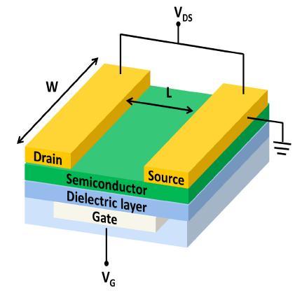
Organicfieldeffecttransistorsareessentiallyathreeterminal device, source drain and gateit is able tobedefined as a sandwichstructuretogetherwithacapacitorwithoneplate asagateandtheotherplateasasemiconductorlayer.The semiconductorlayerinterfaceselectronicallywiththeother twoelectrodes(sourceanddrain).Fig-1showsthesimple diagram of OFETs. A gate electrode is made from a highly dopedsiliconorgold,silverorplatinumconductivematerial depositedonaninsulatingsubstratewhichincludesglass.All different layers are very thin, vaporized or printed films which giveadualreasonof the structural base of the gate device and the carrier gate terminal, as they cannot structurallysupportthemselves.[2]
SiliconGateMaterialSilicondioxideisgenerallyfavoredasa dielectric materials, but printable insulate polymers- for examples,polystyrene,poly(methylmethacrylate)(PMMA) andpolyurethaneandPVVareusedtomakeflexibledevices. Organicsemiconductorlayersmaybeprintedordeposited theuseofphysical vapourdepositionwhichincludespoly (3-hexildiophene-2,5-diol) (P3HT) or pentacene are used. Thesourceelectrodeandthedrainelectrodesaremadeof conductivematerialsuchaspolymerormetal.[3]
International Research Journal of Engineering and Technology (IRJET) e-ISSN: 2395-0056
Volume: 09 Issue: 12 | Dec 2022 www.irjet.net p-ISSN: 2395-0072
Mobilitycanbegivenby, ,
=2
Fig -2: (a) Output characteristic of an OFETS
Threshold voltage is the result of much effect and is powerfully dependent on the organic semiconductor and usingdielectric.Normally,thresholdvoltagecanbecaused bychargetraps,interfacestates,impuritiesinherentdipoles etc. And this can be reducing by increase the gate capacitance, which produces a higher charge at a lesser appliedvoltage.Inmaximumofinstances,theinputvoltage isn'ta given deviceisalwaysconstant.It iscalledthe bias stress performance and it has an important impact at the application of organic transistors in electric circuits. It is thereforecurrentlyunderintensescrutiny.Achangeinthe input voltage might cause current hysteresis on the time scaleofthecurrent-voltagemeasurement.[5]
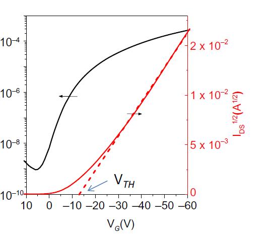
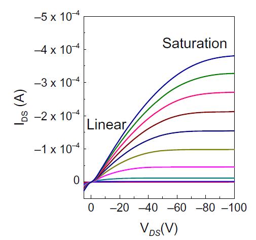
Fig -2: (b) Transfer characteristic an OFETS
Forasmalldraintosourcevoltage,theTransconductance (gm), which is the change in source to drain current with gatetosourcevoltage,canbeusedtoderivethecarrierfieldeffect mobility ( ) in the linear area (VDS). For Transconductance(gm )isgivenby gm=- |VDS=smallconst. = Therefore,thelinearmobility =-gm |VDS=smallconst.
Similarly,thebiaseddevice'stransfercurve(IDS/ VGS) yields the field-effect mobility ( in the saturation stateas[VDS≥VGS-VT]Thefieldeffectmobilitydemonstrates thatthesaturatedcurrent'ssquarerootisonlydependenton gatevoltage.Theslopeofthecurvethatdepictsthesquare rootofthesaturatedcurrentasafunctionofthegatevoltage between the source and gate is where the field-effect dynamicscurveisretrievedfrom(Vgs).[6]
AnyotherimportantFieldEffectTransistor(FET)parameter that can be subtracted from the transfer property is the presenton/offratio.Itisdeterminedbythedrainagecurrent toon-stateandoff-stateratio.Thisvalueneedstobeashigh as it can be for the transistor to operate at its best. The currentonstatealsodependsonthegatedielectricpotential andonthemobilityofthesemiconductorwhenthecontact resistance property at the source electrode and drain electrodes is disregarded. The gate leakage current also affectsthecurrentoffstate.Duetotheconductionchannel on the substrate boundary and the semiconductor's bulk conductivity,thisisextendedforsemiconductorlayersand non-patterngateelectrodes.Additionally,accidentaldoping canboostcurrentoffstate. [7]
Subthreshold swing/subthreshold slope regulates the voltageneededforthetransistortochangefromtheon-state totheoff-state.Tofurtherreducetheoperationvoltages,the sub threshold slope (SS), which specifies the gate voltage quantitynecessarytoincreasethedrain-sourcecurrentby anorderofmagnitudeinthesubthresholdregion,shouldbe steep.ThisishowtheSubthresholdSlopisdefined-
Here,
SS=SS theoretical(1+ )
SS theoretical=In(10)vth=59.6 (atT=300K)
Dt - Trapdensity
International Research Journal of Engineering and Technology (IRJET) e-ISSN: 2395-0056
Volume: 09 Issue: 12 | Dec 2022 www.irjet.net p-ISSN: 2395-0072
vth -Thermalvoltage
C -Gatedielectric’sCapacitance.
ForaperfectOrganicFET,thesubthresholdswingatroom temperature(T=300K)isaround59.6mVdec-1.[23]
Contact resistance, which restricts device performance, is theresistancepresentbetweenthecontactelectrodeandthe semiconductorinterface.Numerousfactors,includingtrap concentration,temperature,theworkfunctionbetweenthe contact electrode and the semiconductor material, doping levels,anddeviceshape,haveanimpactonit.Thebarrier heightisloweredasaresultofincreasingtheworkfunction of the contact electrode, which also lowers contact resistance.Reducedcarriermobilityduetohighresistance drainscurrent.Byincludeanoptimallyconstructedacceptor layer and an appropriate active layer thickness, it can be decreased.
Basically,organicsemiconductorsfallintotwocategories:1. SmallmoleculesPolymers2.Asmallermoleculehasfewer conjugated monomer units than a polymer, which has numerousconjugatedmonomerunitsandoftenformslonger chainswithmorecomplicatedstructures.Theefficiencyof theprocessandthequalitiesofthepolymersareessentially determinedbytheconfigurationofrepeatedmonomerunits. These materials may be sub classified as semiconductors, whichrequiren-typesemiconductor,p-typesemiconductor, andambipolartransportationchannelswhilebeingincluded in OFET, depending on the kind of charge carriers they primarilytransportinequipment.[7]
Overthepast2decades,TheP-typesemiconductormaterial hasmadegreatstridesduetotheireasydesignandartificial approach.P-typeorganicsemiconductorconsistmainly of acins, heterosines, theophanes, and their corresponding polymersandoligomerswithtwo-dimensional(2D)disc-like molecule.[6]
4.1.1.1 Pentacene –Pentacene was first reported as a benchmark for organic semiconductors in the 1970s, although many OFET applications have been conducted recently.[6]ThepentaceneisaP-typesmallmoleculeandit isapolycyclicaromatichydrocarbonwithfivelinearlinked Benzene rings. It is highly composite compound is the organic semiconductors. Excitation is produced by this chemicalwhenultravioletorvisiblelightisabsorbed.Itis extremelyvulnerabletooxidation.Thereforethismoleculeis apurplecolorpowder,decomposesgraduallywhenexposed
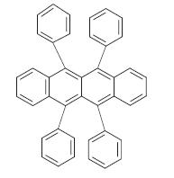
tolightandair.[9]Pentacenemoleculesareknowntohave highcarriermobilityincomparedwithmanyotherorganic compounds. The electrical performance of the pentacene transistors (normally organic transistors) is limited in carriermobility,operatingvoltageandpowerconsumption.
Fig -3: Chemical structure of Pentacene
4.1.1.2 Rubrene – The Rubrene (5,6,11,12tetrafenyltetrazine)moleculeistheredpolycyclicaromatic hydrocarbon.Rubrenisuseasasensitizerinchemistryand alsoasayellowlightsourceinlightsticks.[10]Rubrenisa moleculewithatetracyclinespineandfourattachedphenyl ring. It has high charge mobility. Specifically, roomtemperature hole mobility is measured for rubbers in a single-crystal OFET of the order 20-40 cm2V – 1 s - 1 [1]. Rubreneisbroadlyuseinorganicelectronics,mainlyorganic field-effect transistors and organic light-emitting diodes (OLEDs)[8]
Fig -4: Chemical structure of Rubrene 4.1.1.3 TIPS-Pentacene – TheTIPS-Pentacene is a high puritymoleculeforusedin OFET.Itisgenerallyusedasa small molecule for OFETs application and it has high performance,excellentsolubilityandgoodambientstability intherangeofcommonorganicsolvents-makingiteasyto processinequipment.[9]
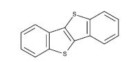
Fig -5: Chemical structure of TIPS-Pentacene 4.1.1.4 DNTT –TheDinaphthothienothiophene(DNTT)isa semiconductingpolymerthathasπ-extendedheteroarenes withsixfusedaromaticrings.Itisathermallystablecrystal thathasaholemobilityof1cm2V-1s-1 whichcanbeusedfora
2022, IRJET | Impact Factor value: 7.529 | ISO 9001:2008 Certified Journal |
International Research Journal of Engineering and Technology (IRJET) e-ISSN: 2395-0056
Volume: 09 Issue: 12 | Dec 2022 www.irjet.net p-ISSN: 2395-0072
majority of electronic applications. It is mainly use in the fabrication of organic field effect transistor (OFET) for a varietyofapplicationssuchasimplantableelectronics,largearea sensitive catheters, and light emitting diodes (LEDs).[10]
based conjugated polymers can potentially be used in combinationwithfullerenesandP3HTforthemanufacture ofawiderangeofdeviceslikeorganicfieldeffecttransistor (OFET),organicphotovoltaics(OPVs),solarcells(SCs)and photodiodes.Ithashighcharge-carriermobilityisapprox∼1 cm2/(Vs)inTFT.Theelectronaffinity(EA)andionization energy(IE)ofPBTTTis−3.2eVand−5.1eV.[13]
Fig -6: Chemical structure of DNTT
4.1.1.5 BTBT -A conjugating polymer, BTBT stands for benzothienobenzothiophene.Itcouldbeaspin-coatedTFT. Itschargemobilityis43cm2V-1s-1 ,makingitissuitablefor usageasp-typesemiconductors.Highfield-effectmobilityin solution-processed OFETs is 5.5 to 5.7 cm2/Vs, and an excessiveOn/Offratio of109ispresent.Theorganiclight emittingdiode(OLED),organicphotovoltaiccell(OPV),and organic thin film transistor are some examples of organic electronicapplicationsinwhichitmightbeused(OTFT).[11]
Fig -7: Chemical structure of BTBT
4.1.2.1 P3HT –TheRegioregularpoly(3-hexylthiophene2,5-diyl)isalsocalledasP3HT.Itisatrendylowbandgap polymersdonorwithapplicationsinOFET,OLED,polymer solar cells and OPV. The highest P3HT polymers produce vastly crystalline film and are suggested for OFET. The regioregularity P3HT and lower molecular weight is recommendedforinkjetanddryingdepositiontechniques for large area where gelling/aggregation and surface roughness should to be avoid. The fabrication report has mobilitymeasurementvalueis0.12cm2/Vs.[12]
Becauseoftheirhighlowestunoccupiedmolecularorbital (LUMO) energy levels, N-type organic semiconductors neverthelessexhibitairinstabilityunderambientconditions despite having much higher mobility than p-type semiconductors. For OFETS, stable n-type semiconductor materialswithhighchargecarriermobilityaretheoptimal choice.
4.2.1 Chemicalstructures of n-type smallmolecules
4.2.1.1 Fullerene -In 1985, the Fullerene tiny molecule was discovered in the sooty residue that remained after carbonwasvaporisedinaheliumenvironment.Theywere given the name "buckminsterfullerenes" in honour of the discoverers who thought that the icosahedral geometry, which contains exactly 60 unsaturated carbon atoms, resembled the geodesic domes made famous by architect Buckminster Fuller. [14] Although the word has been shortened to "fullerene," they are also known as "buckyballs."Twelvepentagonsandtwentyhexagonsmake upthetruncatedicosahedralshapeoffullereneC60.Every vertexandedgeofthepolygonsarejoinedbybondsmadeup ofonecarbonatom.FullereneC60hasanucleus-to-nucleus diameterofaround0.71nmandavanderWaalsdiameterof about1.1nm.[14]
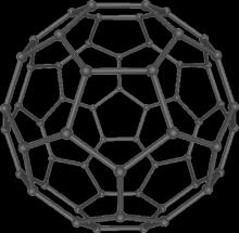
Fig -8: Chemical structure of P3HT
4.1.2.2 PBTTT -PBTTT-C14isasemiconductingmaterial whichisusedasaholetransportingmaterial(HTM).Ithas crystalorientationandorderedstructuregivestheresultin a high performance conducting material.[1] PBTTT-C14
Fig -10: Chemical structure of Fullerene
4.2.1.2PCBM -The fullerene derivative of C60 buckyball, PCBM,wascreatedforthefirsttimeinthe1990s.Inflexible
2022, IRJET | Impact Factor value: 7.529 | ISO 9001:2008 Certified Journal | Page384
International Research Journal of Engineering and Technology (IRJET) e-ISSN: 2395-0056
Volume: 09 Issue: 12 | Dec 2022 www.irjet.net p-ISSN: 2395-0072
electronics, it is frequently combined with P3HT, organic solarcells(plasticsolarcells),orelectrondonormaterials like P3HT or other conductive polymers since it is an electron-acceptingsubstance.[16]Itcombineswithp-type conjugatedpolymertoproducethinfilmorganicfieldeffect transistors and photovoltaic (PV) components (OFET). It facilitates heterojunction PV cell and organic field effect transistorsolutionprocessesaswellascompositesplanning. In a thin-film organic field effect transistor, PCBM has the strongest affinity for effective photo-induced electron transferfromp-typepolymersaswellasmetalelectrodes. Bulk energy conversion efficiency of 4.4% have been reported.[15]
they are suitable for charge transfer, which results in the generationofchargetransferexciton.[17]
Fig -13: Chemical structure of PTCDI
4.2.2 Chemical structures of n-type polymers
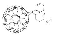
Fig -11: Chemical structure of PCBM
4.2.1.3 NTCDI –TheNaphthalenetetracarboxylicdiamide (NTCDI) is a solid organic compound and simple naphthalenediamides(NDIs).Theintermediatecompound from NTCDI parent naphthalene is produced by naphthaleneetracarboxylicdionehydride. NTCDI RedoxActiveformsastableradicalionat-1.10VagainstFC/Fc+. [5] The ability to accept electrons showcase an extended coupling ring system and the presence of electron withdrawal groups (carbonyl centers). Because of its tendency to form charge-transfer complexes with crown ethersNDIisusedinsupermolecularchemistry,forexample, togiverotaxanesandcatechins.[16]
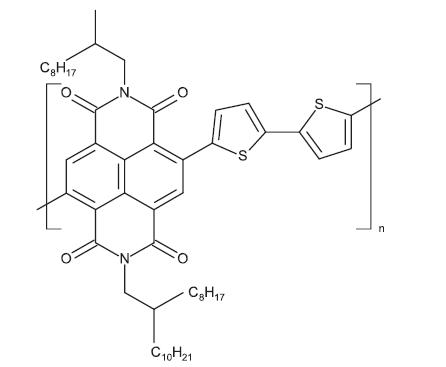
4.2.2.1 P (NDI20D-T2) –Researchers have studied the P(NDI2OD-T2)copolymercomprisingnaphthalenediimide (NDI) and bithiophene units for usage as an electron acceptorinpolymersolarcells.Thepolymerexhibitshigh electron affinity, high light absorption, and excessive electronmobility.AllpolymersolarcellswithJ51asadonor (fullerene-free) and P(NDI2OD-T2) as an acceptor have demonstratedanenergyconversionefficiencyofover8%. AnothernamefortheP(NDI2OD-T2)ishigh-mobilityn-type polymer semiconductors. Based on organic field effect devices,P(NDI2OD-T2)haselectronmobilityrangingfrom 0.45to0.85cm2V-1s-1.[18]
Fig -12: Chemical structure of NTCDI
4.2.1.4 PTCDI – Due to its brilliant colour, fluorescence, and strong absorption as well as excellent thermal and photochemicalstability,theperylenetetracarboxylicdiimide, oftenknownasPTCDI,isfrequentlyusedasacommercial pigment[14].Powerfuln-typeorganicsemiconductorswith severalusesincludePTCDIanditsderivatives.Forinstance, they are used as optoelectronic devices such molecular switches, tunable laser dyes, solar cells, light-emitting diodes, and transistors due to their unique optical and electrochemical capabilities. Due to their significant intermolecular aggregation, derivatives of peryleneetrocarboxylic acid show warning indicators that
Fig -14: Chemical structure of P(NDI20D-T2)
4.2.2.2 BBL -ThePoly(benzimidazobenzophenanthroline) Polymer is a semiconductor with n-type behaviour in photovoltaiccells(PVs)andorganicfield-effecttransistors (OFETs).ThisProcessedfromsolutionsinmethanesulfonic acid.ThechemicalformulaofBBLis(C20H6N4O2)n,andBand gapis1.9eV.ThismaterialhasOrbitalenergyLUMO-4.0eV andHOMO-5.9eV.ThepropertiesofN-typesemiconductor mobilityis0.1cm2/V·sandP-typesemiconductormobilityis 0.4cm2/V·s[19]
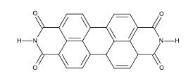
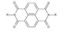
Fig -15: Chemical structure of BBL
2022, IRJET | Impact Factor value: 7.529 | ISO 9001:2008 Certified Journal
International Research Journal of Engineering and Technology (IRJET) e-ISSN: 2395-0056
Volume: 09 Issue: 12 | Dec 2022 www.irjet.net p-ISSN: 2395-0072
Al2O3 Pentacene Spincoating [25]
Al2O3 ZNO D.C. Sputtering [26]
Al2O3 IGZO Anodization [27]
Ta2O5 P3HT e-Beam [28]
HfOx PTCDI-C13 Sol-gel [29]
PVA P3HT Spin-coating [30]
SBA Pentacene Sol-gel [31] TiO2/SAM DNTT Anodization [32]
Conclusion-
In this paper work has been carryout materials study for OFET.Organicfieldeffecttransistorsarethemostimportant technologywiththeuseoforganicsemiconductorandalso polymer.Organicfieldeffecttransistordeviceprovidedhigh flexibility and low manufacturing cost and also large area coveragetransistor.VariousOFETbaseddeviceusingp-type materials which includes pentacene because of higher carriermobilityincomparativeton-typematerials.Itcanbe treated at low temperatures compatible with plastic substrate,whilehightemperatureisneededfordifferentSi based FET. For Low power OFET design reducing Sub threshold Swing and Contact resistance is also decreased. High-k dielectric material should be used to reduce the operating voltage. Organic semiconductors based sensor showgreatbiocompatibilityandselectivityandalsomore sensitivityincomparisontoconventionalsensingdevices.
[1]J.GuidezandG.Prêle,“GeneralDescription,” Superphenix, pp.1–21,2017,doi:10.2991/978-94-6239-246-5_1.
[2] O. Field and E. Transistor, “Lecture # 10 Organic Field EffectTransistor,”pp.1–35.
[3] Kalpana Besar, “Organic Semiconductor Devices for ChemicalSensingandBioInterfaces,”2016.
[4]ParminderKaur,SSGillandBRaj,“ComparativeAnalysis of OFETs Materials and Devices for Sensor Applications”, JournalofSilicon,SpringerMay2021.
[5] Shailendra Singh, B. Raj," Analytical Modeling and SimulationanalysisofT-shapedIII-VheterojunctionVertical T-FET”,SuperlatticesandMicrostructures,Elsevier,Vol.147, PP.106717,Nov2020.
[6]S.Singh,B.Raj,"ModelingandSimulationanalysisofSiGe hetrojunction Double GateVertical t-shaped Tunnel FET”, SuperlatticesandMicrostructures,ElsevierVolume142,PP. 106496,June2020
[7] Sunil Kumar, B. Raj, “Dual-Material Gate-Drain Overlapped DG-TFET Device for Low Leakage Current Design”, Journal of Silicon, Springer, Vol.34, PP. 1-8, July 2020.
[8] G. Information, “Device Structure (OFETs),” pp. 6–10, 2021.
[9]P.Code,“TIPS-Pentacene,”pp.1–8,2021.
[10] R. Categories and L. Information, “General descriptionCerticateofAnalysis,”pp.5–6,2021.
[11]R.Categories,“GeneraldescriptionNotapplicableCerti cateofAnalysis,”pp.1–2,2021.
[12] P. Code and M. Kgaa, “P3HT Sale on End of Line BatchesWhileStocksLast,”pp.1–6,2021.
[13]J.E.Cochran et al.,“Molecularinteractionsandordering in electrically doped polymers: Blends of PBTTT and F4TCNQ,” Macromolecules, vol. 47, no. 19, pp. 6836–6846, 2014,
[14] “Fullerene N-Type semiconductor material,” p. 2021, 2021.
[15]P.Numbers,“PCBM-Basedn-TypeSemiconductors,”pp. 6–11,2021.
[16]“Naphthalenetetracarboxylicdiimide,”vol.4,no.5690, p.5690,2021.
[17]M.El-Nahhas,H.Abdel-Khalek,and E.Salem,“Optical Properties of 3,4,9,10-Perylenetetracarboxylic Diimide (PTCDI)OrganicThinFilmsasaFunctionofPost-Annealing Temperatures,” Am. J. Mater. Sci.,vol.2,no.4,pp.131–137, 2012,doi:10.5923/j.materials.20120204.06.
[18] P.Code,T.Ossila,andM.Information,“PNDI(2OD)2T (highmobilityn-typepolymer),”pp.1–2,2021.
[19]Q.Level,“NotapplicableCerticateofAnalysis,”pp.7–9, 2021.
[20] S. Narahari, D. Bharti, A. Raman, B Raj, “UV Photo Response of Semiconductor: Polymer blend Organic Field EffectTransistors”,IEEEVLSICircuitsandSystemsLetter, Vol.6,issue-4,PP.13-25,Nov.2020.
[21] S Singh, B Raj," Analytical Modeling and Simulation analysis of T-shaped III-V heterojunction Vertical T-FET”, Superlattices and Microstructures, Elsevier, Vol. 147, PP. 106717,Nov2020.
© 2022, IRJET | Impact Factor value: 7.529 | ISO 9001:2008 Certified Journal | Page386
International Research Journal of Engineering and Technology (IRJET) e-ISSN: 2395-0056 Volume: 09 Issue: 12 | Dec 2022 www.irjet.net p-ISSN: 2395-0072
[22] TChawla,MKhosla,BRaj,“OptimizationofDouble-gate Dual material GeOI-Vertical TFET for VLSI Circuit Design, IEEEVLSICircuitsandSystemsLetter,Vol.6,issue-2,PP.1325,Aug2020.
[23]MKaur;NGupta;SKumar;BRaj;ArunKumarSingh, "RF Performance Analysis of Intercalated Graphene Nanoribbon Based Global Level Interconnects" Journal of ComputationalElectronics,Springer,Vol.19,PP.1002–1013, June2020.
[24] G Wadhwa, B Raj, "An Analytical Modeling of Charge PlasmabasedTunnelFieldEffectTransistorwithImpactsof Gate underlap Region" Superlattices and Microstructures, Elsevier,Vol.142,PP.106512,June2020.
[25]F.I.I.Enabled,W.Cai,J.Zhang,J.Wilson,A.Song,andS. Member,“InvertersEnabledbySolution-Processed,UltraThinAl2O3,”2019,
[26]C.Bartic,H.Jansen,A.Campitelli,andS.Borghs,“Ta 2O5 asgatedielectricmaterialforlow-voltageorganicthin-film transistors,”vol.3,pp.65–72,2002.
[27] B. Leszek, A. Majewski, R. Schroeder, and M. Grell, “Low-Voltage ,"High-Performance Organic Field-Effect TransistorswithanUltra-ThinTiO2LayerasGateInsulator,” pp.1017–1022,2005,
[28] A. R. V Benvenho, “semiconductor / insulator for application in low voltage organic field effect transistors Studyofpoly(3-hexylthiophene)/cross-linkedpoly(vinyl alcohol)assemiconductor/insulatorforapplicationinlow voltageorganicfieldeffecttransistors,”vol.214509,2013, doi:10.1063/1.4809285.
[29] B.N.Pal,B.M.Dhar,K.C.See,andH.E.Katz,“Solutiondeposited sodium beta-alumina gate dielectrics for lowvoltageandtransparentfield-effecttransistors,” Nat. Mater., vol.8,no.11,pp.898–903,2009,
[30]M.Sawamoto,H.Sugino,M.Nakano,andK.Takimiya, “High-performance solution-processed organic thin-film transistorsbasedonasolubleDNTTderivative,”pp.1–28.
[31]Y.H.Lee,M.Jang,M.Y.Lee,O.Y.Kweon,andJ.H.Oh, “Flexible Field-Effect Transistor-Type Sensors Based on Conjugated Molecules,” Chem, vol. 3, no. 5, pp. 724–763, 2017,
[32] F.Wikipedia,“Abiosensorisananalyticaldevicefor the detection of an analyte that combines a biological componentwithaphysicochemicaldetector.”pp.1–7,2012.
2022, IRJET | Impact Factor value: 7.529 | ISO 9001:2008 Certified Journal |