International Research Journal
of
Engineering
and
Technology (IRJET) e-ISSN: 2395-0056

Volume: 09 Issue: 12 | Dec 2022 www.irjet.net p-ISSN: 2395-0072
Design and Implementation of Different types of Carry skip adder
1Dept. of Electronics and Communication Engineering, BMS College of Engineering Bangalore, India
2 Dept. of Electronics and Communication Engineering, BMS College of Engineering Bangalore, India
3 Dept. of Electronics and Communication Engineering, BMS College of Engineering Bangalore, India
4 professor, Dept. of Electronics and Communication Engineering, BMS College of Engineering Bangalore, India ***
Abstract - Inmanycomputersystems,addersarethebasic building blocks. The Carry-Skip Adder (CSA) is one of the fastest and most space-effective adder topologies. The existing CSA structure available in the literature is high becauseofitsconventionaldesign.Intheproposedadder, compoundgatesareemployed.Performanceimprovementis observedduetothepresenceofAOIandOAIlogic.8-bitCSA isdesignedandanalyzedusingbothXilinxISE14.2Vivado DesignSuiteandCadence,toanalyzeareaandpower.The design is implemented on a Zed board using Verilog HDL programming.
Key Words: Carry Skip Adder, Common Boolean Logic (CBL), high performance.
1. INTRODUCTION
Thecarryskipadderisanefficientadderwhenitcomesto space and energy usage. Adders are an essential part of arithmeticandlogicalunits(ALUs).Itacceleratesadditionby spreadingacarrybitthroughouttheentireadder.Becauseof itsexcellentcomputingefficiencyandminimaldelay,CSKA attracts a lot of interest. Additionally, due to the minimal number of transistors, the carry skip adder has relatively littlewiringandastraightforwardlayout[1].Thispapergoes intomoreinformationabouttheworkthathasbeendoneto increasethespeedandpowerofCSKA.Betterspeedsmust be achieved with the least amount of power dissipation, whichisdifficultforVLSIdesignerstoachieve.Theanalysis ofanadderutilizingatraditionalcarryskipadderiscovered andexplainsthedesignlogicforCBLaddersarethefastest adderswithareaoverheadarea,whicharealsoefficientin termsofareaandpower[2][3].
Loweringthesupplyvoltageisaveryefficientwaytoreduce a circuit's power consumption. Additionally, power consumption is substantially decreased because the switching energy heavily depends on voltage. [1] We currentlyhavealargenumberofadderswithvaryingdelays and power losses. For instance, carry skip adders (CSKA), parallelprefixadders,ripplecarryadders(RCA),andcarry increment adders (CIA) [2] When it comes to space and energyutilization,thecarryskipadderisanexpertadder.It acceleratesadditionbyspreadingacarrybitthroughoutthe entire adder. Although CSKA has a substantially shorter delay than RCA[3]. Additionally, the carry skip adder has
relativelyshortwiringlengthsandastraightforwarddesign duetoitslowtransistorcountBybreaking theadder into varying-sizedblocksthatbalancethelatencyofinputstothe carrychain,thedelayandpowerdissipationofthecarryskip adder are decreased[5]. It is important to note that the proposed adder's delay improvement was accomplished without increasing power consumption or circuit complexity[6].Inordertoincreasespeedperformance,this paperonlyoffersanoptimizationstrategyforthescenarioof constant block size[7]. A 16-bit carry skip adder has been developed, which is an improvement of the conventional ripple carry adder created via reversible logic[8]. The suggestedcircuitsignificantlyreducesthechipsizeandthe number of transistors[9]. The size of the transistors, parasitic capacitance, and latency in the critical path are described in this study as the design's speed-limiting factors[10].Binary CodedDecimal (BCD)adderandCarry Skip BCD adder implementations for reversible logic are presentedinthiswork[11].Thesedevicesshouldusehighspeed,low-power,andarea-efficientcircuitstoaccomplish the calculations[12]. The technique put forward has been proven effective by using it in the design of more than 50 adderswithdifferentdelaysforthelogicgatesemployedand bit counts[13]. This paper presents a novel technique for findingthebestdistributionwithnolimitonthenumberof skip levels and demonstrate a full-static carry-skip adder with minimal power dissipation and great operation efficiency[14].
2.LITERATURE SURVEY
Smalltechnologicaldevicesarenowanecessarycomponent of daily life. Devices with extremely high speeds and low powerconsumptionareinhighdemand.Themainchallenge in creating high-speed arithmetic units is minimizing the amount of time needed for carrying to propagate through adders. For this issue, numerous solutions have been put forth.Oneofthemusesacarryskipadderratherthanany other adder because it is a fundamental part of every processor.
[1]
Carry Skip Adder Using Blocks of Full Adders
Lehmanetal.madetheinitialsuggestionforthecarryskip adder(CSKA)(1961).Itsspeedwasdiscoveredtobehigher thanthetypicalRCA.Tominimizelatenciesincarryingskip adders, some programs have been implemented. The
International Research Journal of Engineering and Technology (IRJET) e-ISSN: 2395-0056
Volume: 09 Issue: 12 | Dec 2022 www.irjet.net p-ISSN: 2395-0072
language used to present algorithms is T. Blocks of full adders are merged to form a CSKA, which influences the CSKA's overall speed (Chan, Schlag, Thompson, and Oklobdzija,992).ThestudysetsupCSKAandCSLAaddersto achievetheleastamountoflatency.
[2] Carry Skip Adder using Concatenation and Incrementation Schemes
M. Bahadori et al(Bahadori, Kamal, Afzali, Pedram, 2016) representationofaCMOSCSKAstructureshowsthatituses lessenergyandoperatesmorequicklythanatraditionalone. Carry the skip logic is accomplished by substituting compound gates known as OR-AND-invert (OAI) and AND-OR-invert (AOI) for multiplexers. Utilizing incrementation and concatenation methods significantlyimprovesspeed.
[3] Carry Skip Adder using Efficient Full Adders
Themostcrucialfactorsthatneedtobetakenintoaccountin the majority of VLSI applications are latency, power, and area. A quick adder can be used to do this. Comparing differentadders,itwasshownthatcarry-skipaddersdrain morepowerandtakeupmorespacethanRCAaddersbut haveshorterdelays.InthestudybyS.K.Shirakoletal.,Thus, theuseofefficientfulladdersallowsforthesolutionofthe powerandareaproblem.(2014)Parvati,Shirakol,Kulkami, andAkash.
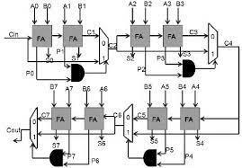
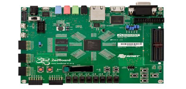
3. ZED BOARD
The Zed Board from Xilinx is a cheap development board thatincludeseverythingrequiredtocreatedesignsbasedon Linux, Android, Windows, or other OS/RTOS. Users can additionally access the processing system and programmable logic I/Os via a number of expansion connectors. Utilize the closely integrated ARM processor systemand7seriesprogrammablelogicoftheZynq-7000 SoC to build creative and effective designs using the Zed Board.
createsthesumusingtheinputbitsforthetwonumbersA andB.The4-bitRCAblock isusedinthedesigned model. Thecarrypredictionunitwilloutputonewhenallofthebits oftherelevantstageareinpropagationcondition.
CSKAdivideswordsthatareaddedtotheblocks.Everyblock has an RCA that generates the carry and sum. However, CSKAshortensthewaittimebyexcludingthegroupofFull stageaddersfromthecarrycomputations.
4. EXISTING ADDERS
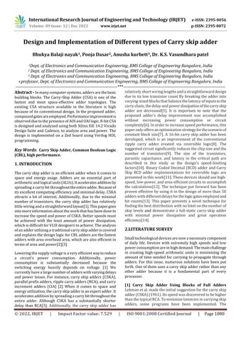
Traditionally,Carryskip-addingiscarriedoutinstages.An RCAblock,amultiplexer,andacarrypredictionunitmake upeachstage.RCAisusedtocalculateeachstage'ssum.It
Figure-1:Carryskip-adderlogicdiagram
Figure 1 illustrates how multiplexers and AND gates are usedtoimplementCSKA'sskipoperation.TheRCAblockand theskiplogicmakeupeachstageinthisscheme.
Figure-2:Simulatedoutputforcarryskip
adder
Inthefigure-2thesimulatedoutputforconventionalcarry skipisproducedusingVerilogincadence.
Figure-3:Schematicoutputofconventionalcarryskipadder
International Research Journal of Engineering and Technology (IRJET) e-ISSN: 2395-0056
Volume: 09 Issue: 12 | Dec 2022 www.irjet.net p-ISSN: 2395-0072
5. PROPOSED TECHNIQUE
Anarea-efficientCSLAissuggestedbysharingtheCommon Boolean Logic (CBL) term in order to eliminate the redundantaddercellsinthestandardCSLA.Theoutputof thesummationsignalisacarry-insignalwithlogic"0"andis an inverse signal of itself with logic "1," according to the analysis of the truth table of the single-bit full adder. To createthesummationpair,whichiswhatCommonBoolean Logiccallsthesummationpair,weonlyneedtodesignone XORgateandoneINVgate.Inordertoconstructthecarry pair,wealsoneedtoimplementoneORgateandoneAND gate. This allows the summation and carries circuits to remainparallel.
required in the circuit is less than that compared to conventionalcarryadders.duetowhichthetotalareaand powerreducecomparedtotheconventionalmethod.
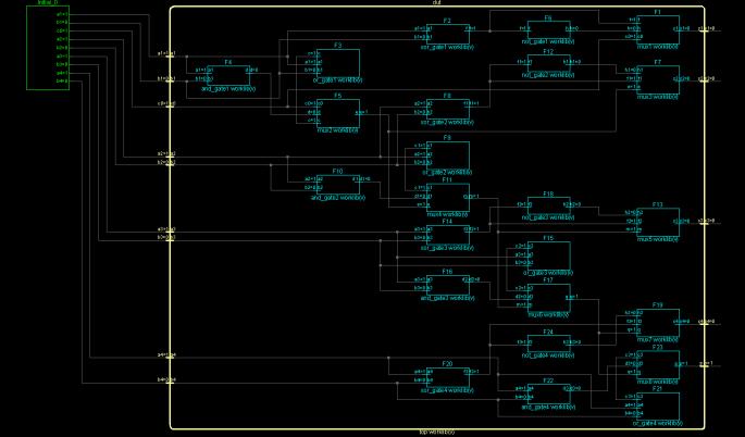
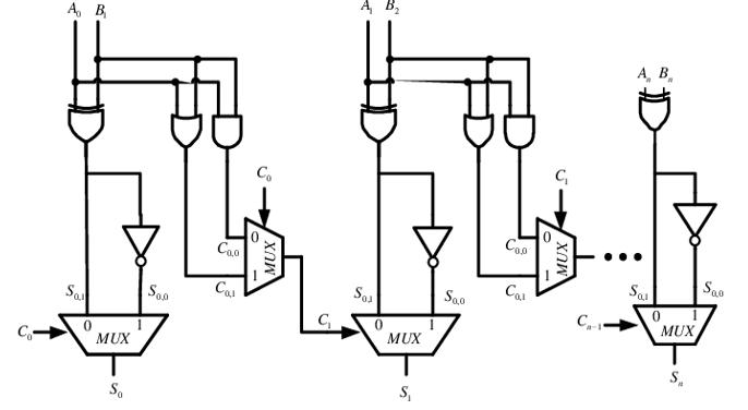
Figure-4:ProposedCommonBooleanLogicDiagram
S=(A B)C’in +(AʘB)Cin
C=(AB)C’in+(A+B)Cin
ItisclearthatMUXbasesitscalculationofthefinalsumon the carry that hasspread from the previous logiccell. The final sum and the carry for the next logic cell are both determinedbythecarrythatwillspread.Thesum(S0)will beS1,0ifthecarrypropagatingfromtheprioradder(C0)is "0,"else,S0willbeS1,1.Inotherwords,thecarrythatmoves tothesubsequentcellwillbeC1,0ifC0is"0,"else,itwill be C1
Figure6:Schematicoutputofconventionalcarryskipadder 6.
RESULTS
7. ThetablebelowshowsthenumberofinputsLUTsanda total number of bonded IOBs. A look-up table, or LUT for short,isessentiallyatablethatdecideswhat theoutputis for any given input (s). It is known as the truth table in combinational logic. Your combinatorial logic behavior is effectivelydescribedbythistruthtable.
Inotherwords,aLUTcanimplementwhateverbehavioryou obtain by connecting any quantity of gates (such as AND, NOR,etc.),withoutfeedbackchannels(toensureitisstateless),andinanydesiredconfiguration.
AnIOBisaninput/outputbuffer.Itessentiallyreferstothe number of pins you have on your gadget. For instance, if yourdesignincludesareset,aclock,an8-bitinput,andan8bit output (all single-ended), you will utilize 1+1+8+8=18 pins,resultingin18bondedIOBs.
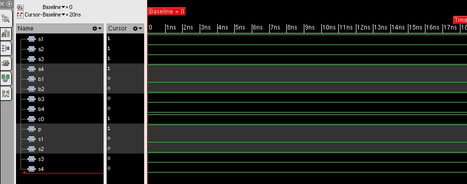
Table 1: ComparisonBetweenConventionalCarrySkip AddersAndCBL.
Adders No. of slices No.ofinput LUTs No. of bondedIOBs Total 8-bit carry skip adders 1 2 18 21 CBL 1 1 10 12
Table-2: Powerandareacomparisonofdifferentadders.
Adders Total power (µW) Totalarea
Figure-5SimulatedoutputforCBL
Intheabove-simulatedoutputofcommonBooleanlogic,it was observed that the number of inputs and outputs
Conventionalcarry skipadder 1.527 86.14 CBL(Thiswork) 0.540719 72.00
International Research Journal of Engineering and Technology (IRJET) e-ISSN: 2395-0056
Volume: 09 Issue: 12 | Dec 2022 www.irjet.net p-ISSN: 2395-0072
Theabovetablebriefsusaboutthedifferenceinthepower andareaofdifferenttypesofaddresses.powerandthearea havereducedinCBLcomparedtothatofconventionalcarry skipaddersthisisduetothereplacementoffulladderswith AOIcircuitsintheCBLcircuits.
8-bitcarryskipaddersusingfulladdersweresimulatedand thetotalpowerandareawerecalculatedusingcadenceand LUT and a number of bonded IOBs were calculated, the obtained results were compared with the total area and power of common Boolean logic circuits. it was observed that the total area and power of CBL are less than that of conventionalcarryskipadders,thisisbecauseinCBLbasic gates were used instead of full adders. Thus the obtained resultsareshowninthetable1andtable2.
7. CONCLUSION
Theproposedadderisdesignedandthesimulationresults are examinedusingtheCadencetool in 45nmtechnology, simulationsofVerilogcodewrittenforcarryskipadderare carriedoutforpowerandareaanalysis.Thesamecodehas beenanalyzedinVivadoDesignSuiteandXilinxISE14.2and implemented on Zed Board. Findings indicate enhanced performance from the suggested adder. Compared to conventionalcarryskipadder64.589%decreaseinpower, an18.737%decreaseoftheareaisvisibleinCBL(Common BooleanLogic).
8. REFERENCES
[1]Low-Power High-Performance Carry Skip Adder: A Review. International Journal of Engineering Applied SciencesandTechnology,2020.
[2]ImplementationOfLowPowerCarrySkipAdderUsing ReversibleLogic-InternationalJournalofRecentTechnology andEngineering-2019
[3]Abhinaya R., Gayathri S., Atchaya S., Kumar G. H. and BalajiG.N.(2019),PowerEfficientCarrySkipAdderBased onStatic125nmCMOSTechnologyinInternationalJournal forInnovativeResearchinScience&Technology,vol.5,(pp. 32-36)
[4]Tale R. and Deshmukh R. M. (2018), Analysis of Low Power High-Speed Carry Skip Adder: A Review in International Journal for Research in Applied Science & EngineeringTechnology,vol.6,(pp.4646-4650).
[5]AroraA.andNiranjanV.(2017),Anew16-bithighspeed and variable stage carry skip adder, in 3rd International ConferenceonComputationalIntelligence&Communication Technology(CICT),Ghaziabad,(pp.1-4).
[6]PatilP.P.andHatkarA.A.(2016),Comparativeanalysis of8-bitCarrySkipAdderusingCMOSandPTL techniques
withconventionalMOSFETat32-nanometerregime,inIEEE 1st International Conference on Power Electronics, Intelligent Control and Energy Systems (ICPEICES), Delhi, (pp.1-5).
[7]PangY.,WangJ.andWangS.(2012),A16-bitcarryskip adder designed by reversible logic, in 5th International Conference on BioMedical Engineering and Informatics, Chongqing,(pp.1332-1335).
[8] Themozhi.G, Thenmozhi. V, Propagation Delay Based ComparisonOfParallel Adders,Journal ofTheoretical and AppliedInformationTechnology.ISSN:1992-8645,E-ISSN: 1817-3195.
[9] Saradindu Panda, A.Banerjee, B.Maji, Dr. A.K. Mukhopadhyay, Power and Delay Comparison in between DifferenttypesofFullAdderCircuits,International Journal of Advanced Research in Electrical, Electronics and Instrumentation Engineering Vol. 1, Issue 3, September 2012,ISSN2278-8875.
[10]BiswasA.K.,HasanM.M.,HasanM.,ChowdhuryA.R. andBabuH.M.H.(2008),ANovelApproachtoDesignBCD Adder and Carry Skip BCD Adder, in 21st International ConferenceonVLSIDesign,Hyderabad,(pp.566-571).
[11] Singh I. and Dhingra M. (2015), Design and Implementation of 32-Bits Carry Skip Adder using CMOS LogicinVirtuoso,Cadence,inInternationalJournalofVLSI System Design and Communication Systems, vol. 03, (pp. 1116-1121)
[12] Alioto M., Palumbo G. (2003), A simple strategy for optimized design of one-level carry-skip adders, in IEEE Trans. Circuits Syst. I Fundam. Theory Appl., vol. 50, (pp. 141-148).
[13]TurriniS.(1989),Optimalgroupdistributionincarry skipadders,inProc.9thIEEESymp.Comput.Arithmetic,(pp. 96-103)
[14] Chirca K., Schulte M., Glossner J., Wang H., Mamidi S. (2004),Astaticlow-power,high-performance32-bitcarry skip adder, in Euromicro Symposium on Digital System Design,DSD,Rennes,France,(pp.615-619).