International Research Journal of Engineering and Technology (IRJET) e-ISSN:2395-0056

Volume: 09 Issue: 11 | Nov 2022 www.irjet.net p-ISSN:2395-0072
International Research Journal of Engineering and Technology (IRJET) e-ISSN:2395-0056
Volume: 09 Issue: 11 | Nov 2022 www.irjet.net p-ISSN:2395-0072
1Dept. of Electronics Engineering, Indira Gandhi Delhi Technical University for Women, New Delhi, India
2 Associate Professor, Dept. of Electronics Engineering, Indira Gandhi Delhi Technical University for Women, New Delhi, India ***
Abstract - In the world of IC, the technology scales down to 32nmor below and CMOS has lost its recommendation during scaling beyond 32nm due tohighpowerconsumptionandhigh leakage current. Scaling triggers Short Channel Effects that can be hard to conquer. So, FinFET is used because it reduces the shortchannel effects. FinFET can be used in thenanometre range. CNTFET is one of the replacements for present CMOS technology because it can provide a stronger control over the thinSi body and reduces the short channel effects. As the full adder isone of the most promising units of the ALU because it reduces speed and power consumption. Thelogicstyle usedfor implementation is a Hybrid CMOS (HC) Full adder which consumes fewer transistors and reduces power. Both technologies (FinFET and CNTFET) reduces short channel effects and can be used in nanometre technologies. In this paper, the main objectiveis to find out the analysis of the best efficient devices between FinFET and CNTFET based on the Hybrid CMOS Full Adder circuit. Here, these are proposed FinFET based Hybrid CMOS Full Adder and CNTFET based Hybrid CMOS Full Adder. These new hybrid adder is having only 10 transistors. The proposed full adder is a CNTFET and FinFET based design implemented using Synopsys tools in 32nm, 16nm, 10nm technology and calculates Power consumption, delay, and Power Delay Product (PDP) are investigated and showed with better result comparison.
Key Words: FinFET, Full Adder, CNTFET, MOSFET, Hybridlogic style
As the technology is scaled down, the electronics market is becoming more competitive, which results in low-powerandlow-energy.VLSIhasbecomeanimportant issueintoday'sconsumerelectronics.Therefore,manyof themanufacturingindustriesare
designedinnanometerrangeforthedemandforcompact, highperformance,lowpower.
Nanometersrangedevicesrestrictedwithaphenomenon like Short Channel Effects which embraces hot carrier effectandtunnelingoveroxidethickness.Toremovethese limitationsweuse twomajortechnologiesi.e,FinFETand CNTFET which have stronger control over the thin Si body.
The addition is one of the most fundamental arithmetic componentsoftheprocessor.Inlowpowerapplications, Full Adder plays the most crucial role in it. Hence, it is veryimportanttoexecutethefulladder circuitwithlow power and high performance. Conventional MOSFETs have been improved for low power and high-speed applications.However,thecharacteristicsofthedeviceare enhanced but there is still remains an issue with high activeleakage.
Therefore,Fin-typeFieldEffectTransistor(FinFET)and CarbonNanoTubeFieldEffectTransistor(CNTFET) has becomethemostpromisingsubstituteforthetraditional MOSFET.Inthispaper,wecomparetheperformancesof FinFET and CNTFET with each other based on hybrid CMOSFullAddercircuitsusingdifferenttechnologies.
Therestofthepaperisarrangedaccordingtothesections asfollows:InsectionII,AnoverviewofFinFET,CNTFET, andHybridCMOSFullAdder.ProposedWorkhasshown in section III. In section IV, schematic design and simulations are presented. Section V analyzed and compareresults.Finally,inSectionVIitisconcludedwith futurework.
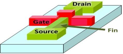
ThefullformofCNTFETisCarbonNanoTubeFieldEffect Transistor.CarbonNanotube(CNT)isaNano-scaletube that contains either a single or an array of carbon nanotubes.Thelayerismadeupofgraphiterolledupinto a cylinder. Depending on the angle and diameter of the foldingitmaybeeithermetallicorsemiconducting.The differences between metallic and semiconducting CNT wouldbedeterminedbychirality
International Research Journal of Engineering and Technology (IRJET) e-ISSN:2395-0056
Volume: 09 Issue: 11 | Nov 2022 www.irjet.net p-ISSN:2395-0072
Fig.1:StructureofCNTFET[1]
CNTsareHexagonalnetworksofcarbonatomsandeach tube acts as a channel whereas, in the MOSFET architecture,thewholesiliconactsasachannel.
CNTFETisa4terminaldevice.
The heavily doped CNT is underneath the drain or the source while the pure CNT is placed under the gate (channel). It carries high drive current, higher transconductanceandithasthesamemobilityinn-type and p-type. CNTFET's V-I characteristics are similar to MOSFET's.
OneoftheadvantagesofusingCNTFETisthatiteasesthe manufacturing process by using a rolled up the hollow cylindricalformofCNTs.Italsoshowsbetterperformance ongate capacitance due to the decrement of source and drain width. It allows for better switching speed and bettershortchannelimmunity.Itrequireslessamountof powerandpropagationdelaywhencomparedtotheCMOS devices.
CNTFET has the potential to mitigate the limitations of Silicon-basedICtechnologywhichhasaphysicallimitto reducethesizeofthedevicestothenanoscaletechnology, dueto its unique structures and magnificent physical & mechanicalproperties.Therefore,CNTFETisconsidered as one of the most promising devices for nanoscale technology.
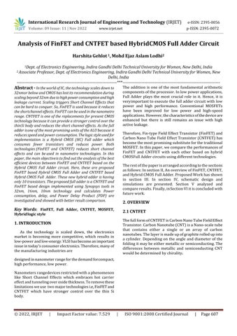
AFinFETwasdevelopedbyBerkleyresearchersofthe University of California. It was designed for use with SOI(Silicon-on-Insulator).FinFETiscategorizedasatype of multi-gate Metal Oxide Semiconductor Field Effect Transistor (MG-MOSFET). A Multi-Gate transistor combinesseveralgatesintoonedevice.FinFETtechnology referstoitsnametothefactthattheFETstructureused lookslikeasetoffins[4].
Fig.2:StructureofFinFET[4]
Inthispaper,weimplementedtheproposedcircuitwith FinFET using the SG Mode configuration. In Short-Gate (SG)mode, the front gate and the back gate are shorted togetherbecauseitwillgivebetterdrivingstrengthtoall overthecircuit.Ifoneoftheinputsgetsexaggeratedthen the operationwould be controlled either by the front or back gate. This typeof mode will help to achieve low leakageanditwillbeimprovedefficiencyalso.
Hybrid logic is the approach that requires using of differenttypesoflogicarchitecture.Theproposed1-BIT fulladdercircuitconsiderablyimprovestheperformance.
The implementation of full adder involves the following expression:
SUM=A⊕B⊕Cin (1)
Cout=A.B+Cin.(A⊕B) (2)
Theimplementationmustbedonebythereductionin transistors and intracellular node connections in comparison to the conventional Full Adder. This proposed circuit can minimize the delay, power dissipation, area, and the overall performance of the circuit. One such implementation can be achieved by using a combination of TG(Transmission Gate) and PTL(PowerTransistorlogic).
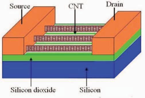
TheconventionalhybridCMOSfulladderarchitecture can besplit into three modules and block diagram is showninfig:3.
Fig.3.BlockDiagramofproposedfulladder[10]
International Research Journal of Engineering and Technology (IRJET) e-ISSN:2395-0056
Volume: 09 Issue: 11 | Nov 2022 www.irjet.net p-ISSN:2395-0072
Modules1and2aretheXNORmoduleswhichgenerate thesum(SUM)signal.TheXNORblockmodulesareused to get better power and require non-complementary inputswhichshowstheperfectoutput.TheCARRYoutput signalisgeneratedbyModule3.Therefore,thesemodules aredesignedtoreducepowerconsumption byusingthe best possible extent that is avoiding the voltage degradationpossibility.
ThereisaLevelRestorationCircuitattheoutputstage. The output signal can get the output with full swings because oftheLevelRestorationCircuit.So,itcanoperate atlowvoltagesandalsoprovidesafull-swingoperation. ThisproposedcircuithasalowerPDPascomparedtothe other types of different architecture. Despite of this, ModulesIIandIIIhavelowPDP.Therefore,thenewadder isexpectedtohavelowpowerconsumption.
The two new full adders consists of less number of transistors,becauseoflessnumberoftransistorsresultsin lessswitchingactivityandarea.
The16THybridfulladdercircuitisimprovedto10T whichisshown in fig 4. Here we are using shorted gate FinFET according to the modes of operation. There are two XNOR circuits using in 10T circuits which are in cascadedform.
Hybridlogicdesignisoneofthelogicdesignsusedfor the implementation of a full adder. The number of transistorscountis10,asshowninfig.5
A,B,andCinaretheinputsandSum&Coutarethe outputs. 10T generates A XOR B and to generate the output, it can be used with its complement as a select signal.ThemainadvantageofusingCNTFETbased10Tis toperformexceptionallygoodatlowertechnologies.Ithas also a smaller delay because of its supply voltage. Meanwhile,theonlydisadvantageofusing10Tfulladder istoproducehighcapacitancevaluesfortheinputs.
Inthiscircuit,thefirstsum signalisgeneratedandthen thecarry-outsignalisgenerated.Thereareintermediate nodes,lower-transistorcount,andhavinglowerloadingof the inputs which helps to generate a balanced Sum and Cout signal. The advantage of using 10T is to reduce powerconsumptionbecausethereisnodirectpathtothe ground.
Fig.5:CircuitDiagramofCNTFETbased10THybridFull Adder
A, B, and Cin are the inputs and Sum & Cout are the outputs. 10T generates A XOR B and to generate the output, it can be used with its complement as a select signal.ThemainadvantageofusingCNTFETbased10Tis toperformexceptionallygoodatlowertechnologies.Ithas also a smaller delay because of its supply voltage. Meanwhile,theonlydisadvantageofusing10Tfulladder istoproducehighcapacitancevaluesfortheinputs.
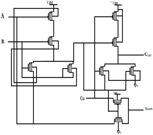
Figure 6 shows the schematic of the conventional 1-bit hybridfulladder.Theproposedadderisdesignedwitha combinationofthreedifferentlogicblocks
International Research Journal of Engineering and Technology (IRJET) e-ISSN:2395-0056
Volume: 09 Issue: 11 | Nov 2022 www.irjet.net p-ISSN:2395-0072
Fig.6:Schematicof HybridFullAdder
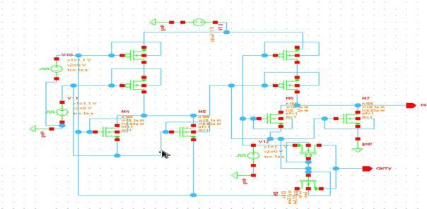
Fig.7:TransientanalysisofHybridFullAdder
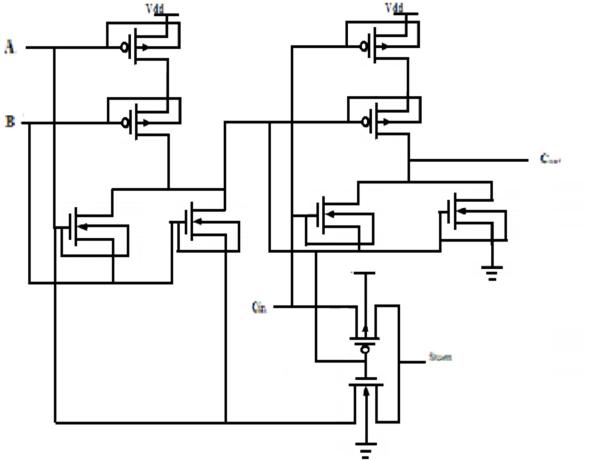
4.2 Finfet based 10T hybrid CMOS Full Adder
Figure8showstheschematicoftheProposed10THybrid fulladder.The16THybridfulladdercircuitisimprovedto 10T, The supply voltage is taken as 0.85 V for FinFET based10THybridFullAdderusingSynopsysToolin16nm technology.
Fig.9:TransientAnalysisofFinFETbased10T HybridFullAdder
4.3 CNTFET based 10T Hybrid CMOS Full Adder
Theresultsofthe10Transistorsimulationcanbeseenin figure 10. The simulation results show the proposed circuit can operate at a higher speed with low power dissipation. The CNTFET based 10T full adder is implementingusingasupplyvoltageof 0.75voltssince 10nmtechnologyisused.
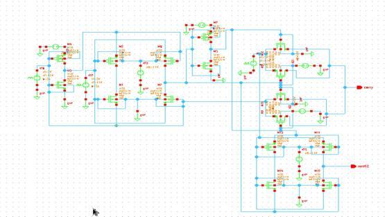
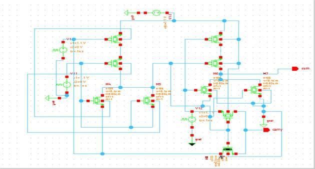
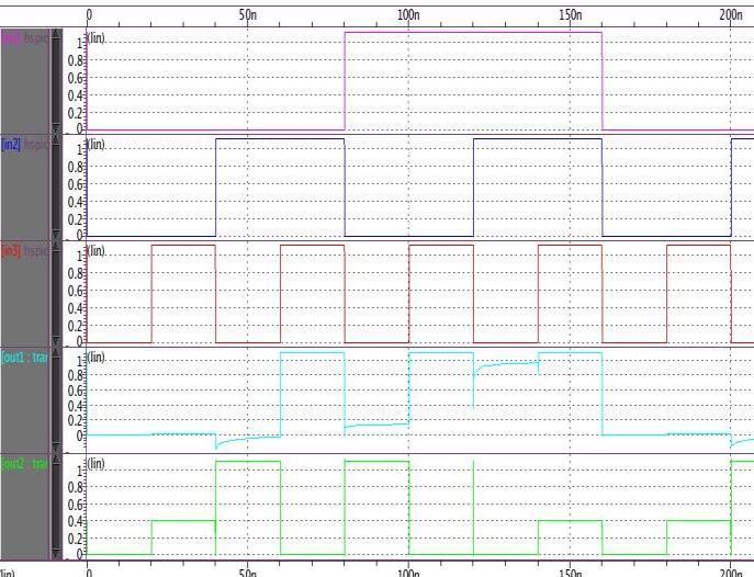
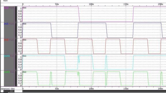
Fig.8:Schematicof FinFETbased10THybridFull Adder
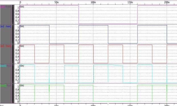
Fig.10:SchematicofCNTFETbased10THybridFull Adder
Fig.11:TransientAnalysisofCNTFETbased10THybrid FullAdder
2022, IRJET | Impact Factor value: 7.529 | ISO 9001:2008 Certified Journal
International Research Journal of Engineering and Technology (IRJET) e-ISSN:2395-0056
Those proposed circuits are compared in terms of power consumption, delay, and the number of transistors used incircuits.
-1:
PARAMETERS Hybrid CMOS FA Proposed FinFET Design FA
Proposed CNTFET Design FA
Technology Used 32nm 16nm 10nm
Supply Voltage 1.1V 0.85V 0.75V Power(uW) 2.079 2.902 1.9420
Delay(ps) 39.5 15.8 6.31
PDP 10^-21 82.8315 45.8516 12.2540
Fromtheoutputwaveform,calculatethevaluesofpower, delay,andpowerdelayproduct.Powerconsumptionand delaytimebotharelowestforCNTFETbasedHybridFull Adder.
TheFinFETbasedHybridFullAdderalsohaveaverylow delaycomparisonto HybridCMOS FullAdder.
CNTFET Based Hybrid Full adder has low power consumption and low delay comparison to both Hybrid CMOSFullAdderandFinFETbasedHybridFullAdder.
Theresultsshow thattheCNTFETHybridFAis93% less than the power consumed by Hybrid FA whereas CNTFETHybridFAis66%lessthanthepowerconsumed byFinFETHybridFA.TheDelayofCNTFETFullAdderis reducedto39%comparedtoFinFETbasedHybridCMOS FA whereas CNTFET Full Adder is reduced to 15% comparetoHybridFA.CNTFETFullAdderisreducedto 26%and14%toFinFETFullAdderandHybridFullAdder.
InthisPaper,FullAddercircuitsareimplementedby using FinFET and CNTFET Technology Simulated in SYNOPSYS TOOLS using 32nm,16nm and 10nm Technology with the supply voltage of 1.1 V, 0.85 V and 0.75V.OneofthelogicstylethatishybridCMOSmodeling our proposed circuit. Thistype of logic design allows designerstooperateflexiblyontheCMOSregiontoachieve the overall performance of a circuit. Most conventional addersshowedlower powerconsumptionatlowvoltage and higher power consumption at high voltage, but our proposed model surmounted this obstacle and showed lowerpowerconsumptioninalltypesoftheinputvoltage. Theaugmentation of efficiency, delay, and Time delay
product(PDP)willbeseenbyabroadcomparisonofall designs.
Using the designed 1-bit full adder blocks, we can design the 2-bit, 4-bit, 8-bit, 16-bit, 32-bit, 64-bit Adder/Subtractor circuits, and so on. Besides that, the performanceandpotentialofotherlogicstylesshouldbe explored in future work. We can even design and compare these designs in all possible Nanometer technologiesbeyond7nm.
Volume: 09 Issue: 11 | Nov 2022 www.irjet.net p-ISSN:2395-0072 © 2022, IRJET | Impact Factor value: 7.529 | ISO 9001:2008 Certified Journal | Page611
[1] S.M.IshraqulHuq,MaskuraNafreen,TasnimRahman and Sushovan Bhadra,“ “Comparative Study of Full Adder Circuit with 32nm MOSFET, DG-FinFET and CNTFET”, International Conference on Advances in ElectricalEngineering28-30September,2017.
[2] P. Sushma Sri Naga Mowlika, V.Srinivasa Rao, “ An EfficientandHighSpeed10TransistorFullAdderswith Lector Technique”, IOSR Journal of Electronics and CommunicationEngineering(IOSR-JECE)-2017.
[3] User Guide on Stanford University Carbon Nanotube FieldEffectTransistors(CNFET)HSPICEModelv.2.2.1. To download model, please visit: https://nano.stanford.edu/stanford-cnfet-model
[4] Jitendra K. S, Avireni Srinivasulu, Brahmadeo Prasad Singh,“A New Low-Power Full Adder Cell For Low VoltageUsingCNTFETs”,(ICECAI)-2017.
[5] M.VamsiPrasad,K.NareshKumar,“LowPowerFinFET Based Full Adder Design”, International Journal of Advanced Researchin Computer and Communication Engineering ISO 3297:2007 Certified Vol. 6, Issue 8, August2017.
[6] JitendraK.S,AvireniSrinivasulu,SM-IEEE,Brahmadeo Prasad Singh “ A New Low-Power Full-Adder Cell For LowVoltageUsingCNTFETs”,ECAI2017-International Conference – 9th Edition Electronics, Computers and ArtificialIntelligence29June-01July,2017.
[7] Smt.A.Nagamalli,N.VivekNagaBhushanam,O.Nagasai, P.Swathi, “Design and Implementation of 4-Bit ALU using FinFET Technology”, International Journal of Innovative Researchin Computer and Communication EngineeringVol.5,Issue5,May2017.
[8] A.Nivetha,M.Hemalatha,“ PerformananceAnalysisofa 1-bitFullAdderusing45nmtechnology”,International Journal of Future Innovative Science and Engineering Research–June2016.
[9] SugandhaChauhan,TriptiSharma,“FullAdderCircuits usingStaticCmosLogicStyle”,InternationalJournalof Computer Applications National Conference on Latest
International Research Journal of Engineering and Technology (IRJET) e-ISSN:2395-0056
Initiatives& Innovations in Communication and Electronics(IICE2016).
[10] NeerajKumarNiranjan,RajendraBahudarSingh,Naviad Z.Rizvi,“Parametricanalysisofahybrid1-bitfulladder in UDSM and CNTFET Technology”, International ConferenceonElectrical,Electronics,andOptimization Techniques(ICEEOT)-2016.
[11] Mr. Kapil Mangla, Mr. Shashank Saxena, “Analysis of Different CMOS Full Adder Circuits based on various parametersforlowvoltageVLSIdesign”,International JournalofEngineeringandTechnicalResearch(IJETR)2015.
[12] M.Madhu,S.KeshavRao,“ANewDesignofLowPower High Speed Hybrid CMOS Full Adder”,International JournalofEngineeringScienceandComputing(IJESC)2015.
[13] RaghavGuptaandAshwaniK.Rana,“Comparativestudy ofdigitalinverterforCNTFETandCMOStechnologies,” NirmaUniversity International Conference on Engineering(NUiCONE),IEEEConferencePublications, 2013.
[14] Sushil B. Bhaisare, Sonalee P. Suryawanshi, Sagar P. Soitkar, “Design of Low Power One-Bit Hybrid-CMOS FullAdderCells”,InternationalJournalofEngineering TrendsandTechnology(IJETT)-Volume4Issue5-May 2013.
[15] Richa Saraswatal, Shyam Akashe and Shyam Babu,“DesigningandSimulationofFullAdderCellusing FinFET Technique” Proceedings of 7th Intl. Conf. on IntelligentSystemsandControl(ISCO)-2013.
[16] Foroutan, Vahid, MohammadReza Taheri,Keivan Navi, andArashAziziMazreah."DesignoftwoLow-Powerfull addercellsusingGDIstructureandhybridCMOSlogic style",IntegrationtheVLSIJournal,2013.
[17] Mohammad Shamim Imtiaz, md Abdul Aziz Suzon, mahmudur Rahman, “Design Of Energy-Efficient Full Adder Using Hybrid- Cmos Logic Style, International JournalOfAdvancesInEngineering&Technology,Jan 2012.
[18] PrateekMishra,AnishMuttreja,andNirajK.Jha,“FinFET CircuitDesign”,NanoelectronicCircuitDesignJha,N.K; Chen,D(Eds.)2011.
[19] ShivShankarMishra,AdarshKumarAgrawalandR.K. Nagaria, “A Comparative Performance Analysis of Various CMOS Design Techniques for XOR and XNOR Circuits”, International Journal on Emerging Technologies2010.
Volume: 09 Issue: 11 | Nov 2022 www.irjet.net p-ISSN:2395-0072 © 2022, IRJET | Impact Factor value: 7.529 | ISO 9001:2008 Certified Journal | Page612
[20] K.K.ChaddhaandR.Chandel,”DesignandAnalysisofa Modified Low Power CMOS Full Adder Using GateDiffusion Input Technique”,Journal of Low Power Electronics,2010
[21] S. Wairya “Ultra Low Voltage High Speed 1-Bit CMOS Adder”.IEEEInternationalConferenceonPower,Control andEmbeddedSystems2010.
[22] Dag. T. Wisland “Ultra Low Power Full Adder Topologies”.IEEEInternationalSymposiumonCircuits andSystems2009,pp.3158-3161.
[23] M. Shams, T.K. Darwish, M.A. Bayoumi, Performance analysisoflow-power1-bitCMOSfulladdercells,IEEE Transactions on Very Large Scale Integration (VLSI) Systems10(1)(2002)20–29.
[24] D.Radhakrishnan,“Low-voltagelow-powerCMOSfull adder,”inProc.IEEECircuitsDevicesSystems,vol.148, FEB2001,pp19-21.