International Research Journal of Engineering and Technology (IRJET)

e-ISSN: 2395-0056
Volume: 09 Issue: 11 | Nov 2022 www.irjet.net p-ISSN: 2395-0072
e-ISSN: 2395-0056
Volume: 09 Issue: 11 | Nov 2022 www.irjet.net p-ISSN: 2395-0072
Aswathy K B1 , Neetha John, Beena M Varghese, Dinto Mathew2
PG Scholar, Dept. of EEE, Mar Athanasius College of Engineering, Kothamangalam, Kerala, India1 Professors, Dept. of EEE, Mar Athanasius College of Engineering, Kothamangalam, Kerala, India2 ***
ABSTRACT: High step-up gain DC-DC converters are becoming increasingly important as the use of renewable energy grows. When circuit complexity taken into account, the quadratic boost converter provides the best trade-off in the cascade boost family. At a moderate duty ratio, this converter can step up a low source voltage to a high voltage, which is more than a conventional boost converter. The quadratic following boost converter in between the source and load appears like a cascaded connection of Switched L-C and Charge pump effect from boosting point of view. The operating principle and the mathematical model of the converter in continuous conduction mode (CCM) are given. In order to provide improved gain, the converter is employed with switched inductor concept. The converter’s superiority is mostly based on the low magnetic field energy, which reduces the size and cost of the inductors and lessens the current stress on the switching elements, resulting in minimal conduction losses that can raise the converter’s efficiency. Besides to illustrate the advantages of designed converter, a comparison with quadratic boost converter is carried out. The performance study and analysis of switchedinductor based quadratic following boost converter is carried out with MATLAB/SIMULINK 2020b for an output power of 500W. The experimental validations for the performance and working of the 3W designed prototype are presented.
KEYWORDS: BoostConverter,Transformerless,Gain,Efficiency,DC-DCconverters,Switchedinductor
A DC-to-DC converterisreferredtoasa boostconverteriftheoutputvoltageishigherthanthesourcevoltage. Aboost converter is sometimes called a step-up converter because it increases the source voltage. The boost converter can be powered from any suitable DC source, such as batteries, solar panels, rectifiers, and DC generators. The process of convertingoneDCvoltagetoanotherDCvoltageiscalledDCtoDCconversion.Boosttopologiesaremorefrequentlyused for high voltage realization, and their range of applications is substantially greater. Enhanced battery pack voltage is necessary in many applications. Due to its ease of operation and ease of construction, the step-up boost topology is a crucial choice for achieving this objective. But if the battery pack voltage is increased excessively, efficiency decreases. Thefunctioningoftraditional boosttopologiesathighdutyratiosistheprimarycauseofthislow efficiency.Duetothe non-ideal resistance present in the converter system, such operation results in increased dissipation losses. Raising the battery pack voltage has the overall effect of decreasing device efficiency and increasing thermal loading, which necessitatesimprovedheatsinkheatextractionsystems.DuetotheshorttransistorswitchOFFtime,thehighdutyratio alsorestrictstheconverter’sswitchingfrequency.Sincethediodehaslesstimetoconductduetothehigh dutycycle,the diode current is reduced to a narrow pulse with a high instantaneous value. In turn, this high diode current results in disconnectedreverserecoverylossandanEMIissue.SeveralnoisolatedDC-DCconvertertopologieshavebeenreported inordertoaddresstheseproblems,whichstill existinconventional convertersbelongingtotheboosttopology class.A novel dual-stage boost converter known as a quadratic boost converter offers the same voltage gain as connecting two boostconvertersinseries.However,comparedtobasicboostconverters,thesesystemsfeatureadditionalL-Celements, whichareprimarilyutilizedtostoremoreenergy,allowingforhigherboostvoltages,aswellastoreduceripplecontent atheavyloads.Ahigh step-upconverter[3]consisting ofanintegratedquadraticboostconverteranda voltage double The integration of the quadratic boost converter makes the system easier to lift up its voltage gain through slightly increasingthedutyratioof thesingleswitch. Thevoltagedoublefurtherincreases thevoltagegainofthesystemasthe turnratiorises.Thevoltagestressesontheswitchandthediodesaredecreasedforsuchcascadedtopology.Theleakage inductancecontributestorealizingzerocurrentswitchingofthediodesinthesecondbooststageandthedoubleandthe energycanberecycledtotheload.Butithascomplicateddesign.AwidevoltagegainDC-DCconverter[4]toincreaseand equalizetherelativelylowvoltageoffuelcellstackswithDClinkbusorenergystoragedevices,suchassupercapacitors or batteries. This introduces two new non-isolated DC-DC converters suitable for such applications, which can be extendedtootherelectricvehiclesaswell.Theconverterscombinethemaincharacteristicsofbothquadraticboostand cuk converters, offering high step-up voltage and control simplicity using only one ground referenced active power switch. Additionally, the topologies present reduced voltage stress across the active power switch when compared to other boost converters. A novel step-up converter [5] with stackable switching stages that is suitable for renewable energyapplications.Ontheonehand,theconvertergaincorrespondstothatofthetraditionalquadraticboostconverter,
© 2022, IRJET | Impact Factor value: 7.529 | ISO 9001:2008 Certified Journal | Page322
e-ISSN: 2395-0056
Volume: 09 Issue: 11 | Nov 2022 www.irjet.net p-ISSN: 2395-0072
achievinganarbitraryexponentialgaininextendedconfigurations.Onotherhand,theconverterrequiresasingleswitch, while the output voltage is partitioned among several capacitors. As argued in this work, the features of this topology representasignificantcontributionwithrespecttostandardtopologiesthatexhibitgreatervoltagestress.Anon-isolated quadratic boost converter [6]featuringlow outputvoltageripple compared toCQBC.Thisadvantagediffersfromother topologiesthatrequirehighamountsofstoredenergycapacitorstoachievethesameoutputvoltageripplespecification.
This property allows for a compact converter design where the size of the capacitors is proportional to their energy storagerating.Solutionforphotovoltaicmodulepartialshading:boostconverter[7]withhighDCgain.Bysubstitutinga switched inductor branch for the boost converter’s inductor, the switched inductor boost converter is created. The conversiongainratiomightberaisedasaresult.InordertoconnectthePVsystemandtheload,thisconverterisused.
Additionally,havingmoreL-Ccomponentsallowsforgreaterdutyratioadjustmentflexibility,whichisnecessaryforthe converter to operate reliably.Additionally,lower duty ratiosare adequateto achievehigh voltage lifting. In the current work,a boostconverter isintroduced thatcloselytracksthevoltagegain ofa quadraticconverter. ASwitched Inductor basedQuadraticFollowingBoostConverterisintroducedforapplicationsthatrequire high-voltagegainasinthecaseof renewable energy applications. In order to provide improved gain, the converter is employed with switched inductor concept.Theconverter’ssuperiorityismostlybasedonthelowmagneticfieldenergy,whichreducesthe sizeandcostof the inductors and lessens the current stress on the switching elements, resulting in minimal conduction losses that can raisetheconverter’sefficiency.
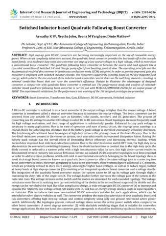
SwitchedinductorbasedquadraticfollowingboostconvertercanboostalowerinputDCvoltagetogreatervaluesatthe load side at trade-off duty ratios than the conventional boost converter. From a boosting perspective, the quadratic followingboostconvertersituatedbetweenthesourceandtheloadresemblesacascadedconnectionofSwitchedL-Cand Charge pump effect. In order to provide improved gain, the converter is employed with switched inductor concept. Switchedinductorbasedquadraticfollowingboostconverterconsistoftwoswitches S1&S2 fivediodesD1,D2,D3,D4 &D5 three capacitors C1, C2 &C3 and three inductors L1, L2& L3 for transferring of power along with load voltage boosting action.Vin istheinputvoltage.outputvoltageisdenotedas VO.Fig.1showsacircuitoftypicalarrangementofswitched inductor based quadratic following boost converter. The converter performance is analyzed under the steady state and continuousconductionmodeconditions.
Theworkingofthecircuitcanbeexplainedbytwomodesofoperation.
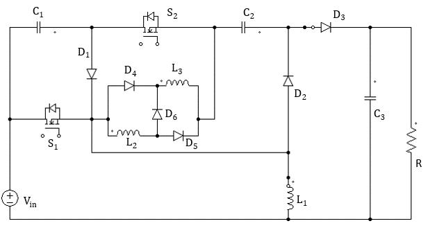
Mode1:Inthismode,switchS1&S2 isturnedon.AtthesametimediodeD2,D4 &D5 isturnedonanddiodesD1,D3 &D6 are turnedoff.TheinputvoltagechargestheinductorL1.ThecapacitorC1 isdischargetochargeinductorL2&L3.Thecapacitor C3 isdischargetosupplyloadR.Fig.3(a)showstheequivalentcircuitdiagramofthe converterandcurrentpathsforthis modeisalsoshown.
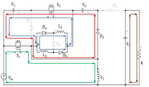
Mode2:Inthismode,switchS1&S2 isturnedoff.AtthesametimediodeD2,D4 &D5 isturnedoffanddiodesD1,D3 &D6 are turned on. The input voltage charges the capacitor C1. The capacitor C2, L2& L3 discharge to charge capacitor C3 and to supply load R. Fig. 3(b) shows the equivalent circuit diagram of the converter and current paths for this mode is also shown.
International Research Journal of Engineering and Technology (IRJET) e-ISSN: 2395-0056
Volume: 09 Issue: 11 | Nov 2022 www.irjet.net p-ISSN: 2395-0072
(a) (b)
Fig.3OperatingModes.(a)ModeI;(b)ModeII
Inordertooperateaconverterproperly,itscomponentsshouldbedesignedappropriately.Someassumptions aretakenforthedesignofswitchedinductorbasedquadraticfollowingboostconverter.Itconsistsofdesignof loadresistance,inductorsL1,L2&L3 andthecapacitorsC1,C2,&C3.Theinputvoltageistakenas42V.Theoutput power and output voltage are taken as 500W and 250V respectively. Switching frequency is 100kHz. So, the ripple of inductor current is taken as ∆IL1 < 30% of IL1, ∆ IL2 < 15% of IL2, and ∆ IL3 < 15% of IL3
Duty Ratio can be found by (1) which is taken as 0.54. The value of load resistor is set as 300Ω in(2).
(1) (2)
The inductors L2 & L3 are obtained by taking current ripple as 15% of IL2 and IL3. By substituting values to (4) & (5) it is approximated to 800µH.each. For inductor L1 the current ripple is 30% of IL1. It is given in (3) and value chosen to be 150µH (3) (5)
(4)
International Research Journal of Engineering and Technology (IRJET) e-ISSN: 2395-0056
Volume: 09 Issue: 11 | Nov 2022 www.irjet.net p-ISSN: 2395-0072
The design of the capacitor mainly considers the voltage stress and maximum acceptable voltage ripple across it. By substituting values to (6) capacitor values are approximated to C1, C2 = 66µF. To ensure sufficient energy and hold up time provided for the post stage, the output capacitor is selected (7) as 100µF
(6)
(7)
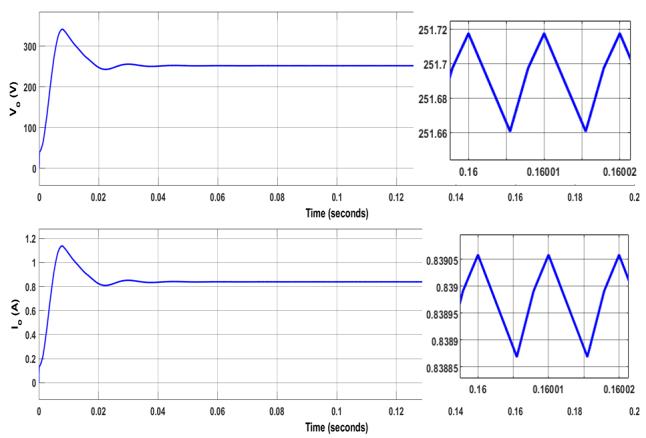
ThequadraticfollowingboostconverterissimulatedinMATLAB/SIMULINKbychoosingthe parameterslistedinTable1. TheswitchesareMOSFETwithconstantswitchingfrequencyof100kHz.ThedutycycleofswitchistakenasD=0.54. Fig. 4(a)showsthattheinputvoltageVin is42VandtheinputcurrentIin is6.1A.Theripplecontentininputcurrentis0.003A. Fig. 4(b) shows the output voltage VO and current IO, VO measured as 251.8V and voltage ripple is 0.06V. The output currentIO is0.83A.
Fig. 5(a) shows gate pulse and voltage stress across the switch S1. The duty ratio of S1 is 0.54. The voltage stress across switch S1 is 92.12V. Fig. 5(b) shows gate pulse and voltage stress across the switch S2. The duty ratio of S2 is 0.54. The voltagestressacrossswitchS2 is214V.Theswitchingfrequencyischosentobe100kHzforbothswitches.
Fig.6showscurrentthroughinductorL.TheinductorcurrentIL1 ismeasuredas4.95A,IL2 is1.46AandIL3 is1.46A.
TABLEI
SimulationParametersofTransformerlessGrid-ConnectedBoostInverter
International Research Journal of Engineering and Technology (IRJET) e-ISSN: 2395-0056
Volume: 09 Issue: 11 | Nov 2022 www.irjet.net p-ISSN: 2395-0072
(a) (b)
Fig.4(a)InputVoltage&InputCurrent,(b)OutputVoltage&OutputCurrent (a) (b)
Fig.5.GatePulseandVoltageStressof(a)S1(VS1),(b)S2(VS2)
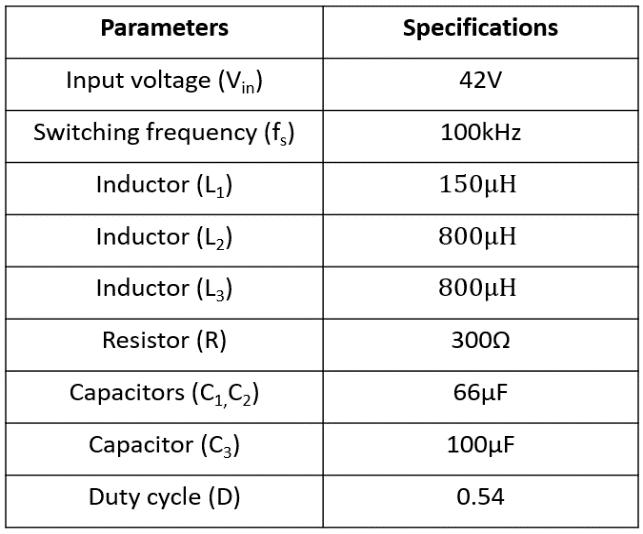
Fig. 7 shows Voltage across capacitors. VC1 is measured as 91.31V, VC2 is measured as 87.94V and VC3 is measured as 251.8V.
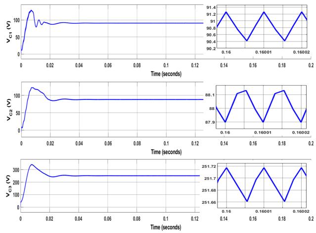
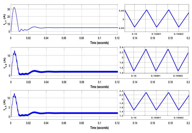
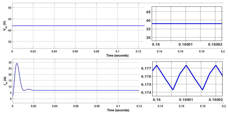
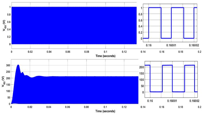
Fig.6.VoltageacrossCapacitorVC1,VC2 &VC3 Fig. 7. Current across Inductors iL1, iL2 & iL3
International Research Journal of Engineering and Technology (IRJET) e-ISSN: 2395-0056
Volume: 09 Issue: 11 | Nov 2022 www.irjet.net p-ISSN: 2395-0072
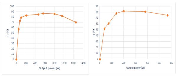
Analysis of quadratic boost Converters is carried out by considering parameters like efficiency, voltage gain, ripple voltage and duty cycle. Efficiency of a power equipment is defined at any load as the ratio of the power output to the powerinput.Itgives,thefractionoftheinputpowerdeliveredtotheload.Thequadraticfollowingboostconverterhas anefficiencyof82%forRloadand70%forRLloadwithanoutputpowerof600W.ThenewSwitchedinductorbased quadratic following boost converter efficiency is around 90% for R load and RL load is around 80% at 180 W output power.TheplotofefficiencyVsoutputpowerforRloadandRLloadisshowninFig.8(a)&(b)respectively (a) (b)
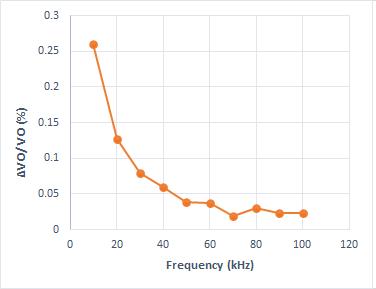
Fig.8.EfficiencyVsOutputPowerfor(a)Rload,(b)RLload
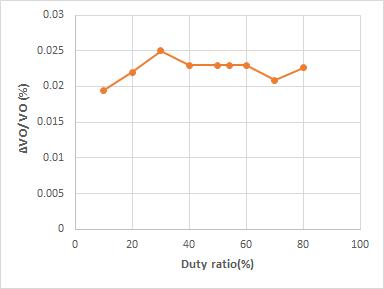
The plot of voltage gain of the converter and duty ratio shown in Fig. 9(a). By analyzing the graph it is clear that the voltage gain increases with Duty ratio for both the converters. The new switched inductor based quadratic following boostconverterhas highgainthanthequadraticfollowingboostconverterforsamevalueofdutyratio. Theanalysisof output voltage ripple Vs switching frequency is shown in Fig. 9(b). According to the analysis the output voltage ripple decreases with increase in switching frequency for both the converters. As increase in switching frequency the % of ripple is low for switched inductor based quadratic following boost converter than the quadratic following boost converter.Thevoltagerippleisminimumat100kHz.FromFig. 10thedutyrato0.54giveslowestripple.Soat0.54duty ratiothehighvoltagegainobtainedis6forswitchedinductorbasedquadraticfollowingboostconverter.
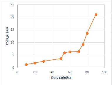
Fig.9 (a)VoltageGainVsDutyratio,(b)OutputVoltageRippleVsSwitchingFrequency
International Research Journal of Engineering and Technology (IRJET) e-ISSN: 2395-0056
Volume: 09 Issue: 11 | Nov 2022 www.irjet.net p-ISSN: 2395-0072
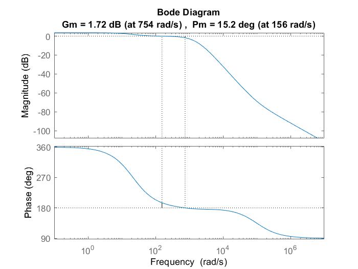
ThebodeplotofsystemisshownintheFig.11.Thesystemhasacontinuous-timetransferfunctionwhichisgivenin(9). TheobtainedPhasecrossoverfrequency(Wpc)is754rad/sandgaincrossoverfrequency(Wgc)is156rad/s.Thus,itcan beseenthatbothpolesarelyingonlefthalfofsplane.Also,both gainmargin(Gm)andphasemargin(Pm)are1.72dB and15.2deg.SobotharepositivevaluesandtheWpc >Wgc.Hence,thesystemisstable. (25.88)��4+(2.592)��3+(1.709)��2 (1.712)��+4.5 ��5 (226.1)��4 - (6.622)��3 +(1.287)��2+(1.71)�� (3.004) (9)
G(s)=
Thecomparisonbetweenquadraticfollowingboostconverterandswitchedinductorbasedquadraticfollowing boost converter is given in Table 2. From the comparison table it is clear that the switched inductor based quadraticfollowingboostconverterhashighefficiencythanquadraticfollowingboostconverter.Thenumber of components higher for modified converter because of the addition of switched inductor in quadratic followingboostconverter.Andtherebythevoltagegainoftheconverterincreasedfrom3.57to6.Theoutput voltage of the converter increased to 251.8 V from 150.3 V. Input and output current also increased. Output voltageandoutputcurrentrippleforboththeconvertersarenearlysame.Thevoltagestressacrossswitchin modifiedcircuitisslightlyhigherthanthatofthenon-isolatedconverter.Table3showsthecomponentswise comparison between switched inductor based quadratic following boost converter and other quadratic boost convertertopologies.
International Research Journal of Engineering and Technology (IRJET) e-ISSN: 2395-0056
Volume: 09 Issue: 11 | Nov 2022 www.irjet.net p-ISSN: 2395-0072
TABLEII
ComparisonBetweenQuadraticFollowingBoostConverter&ProposedConverter
ComparisonBetweenSwitchedInductorbasedQuadraticFollowingBoostConverter&OtherInverters


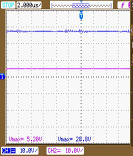
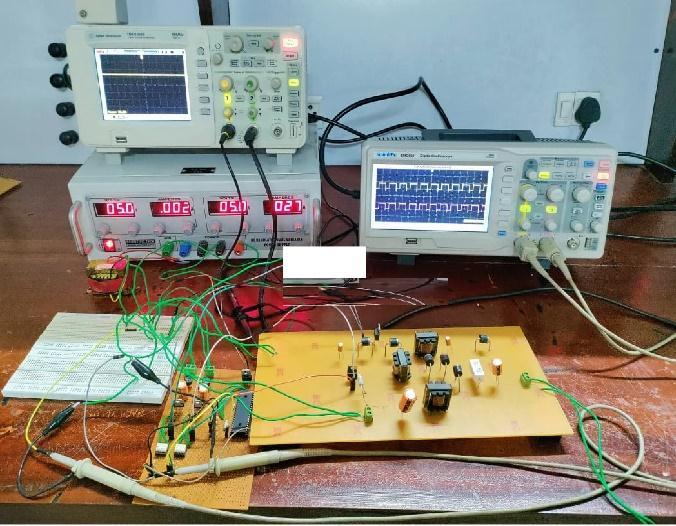
For implementing hardware, the input voltage reduced to 5V to obtain the output of 29.7V with output power of 2.9W. TheswitchesareMOSFETwithconstantswitchingfrequencyof100kHz.ThedutycycleofswitchistakenasD=0.54.The experimentalsetupofswitchedinductorbasedquadraticfollowingboostconverterisdonethroughtwostages.Firstthe programiswritteninmicro-Cforgeneratinggatepulsesforswitchingdevices.Theprogramisverifiedandfrequencyis checkedbysimulatingitintheProteussoftware.Theprogramisburnedtothemicrocontroller (PIC16F877A)usingthe software micro programming suit for PIC. The switches used are MOSFET IRF540 along with its driver TLP250. ExperimentalsetupofswitchedinductorbasedquadraticfollowingboostconverterisshowninFig.11(a).Theoutputof 28.8V is obtained by drawing an input current of 0.008A. Fig. 11(b) shows the output waveform of the proposed converter.
International Research Journal of Engineering and Technology (IRJET) e-ISSN: 2395-0056
Volume: 09 Issue: 11 | Nov 2022 www.irjet.net p-ISSN: 2395-0072
Aswitchedinductorbasedquadraticfollowingboostconverterandconsiderableconversionratioispresented.Switched inductorconceptisadoptedinordertoimprovethegain. Bychargingtheinductorsinparallelanddischarginginseries thegainisimprovedto6.Theconverter’ssuperiorityismostlyduetothelowmagneticfieldenergy,whichreducesthe size and cost of the inductors and reduces the current stress on the switching parts, resulting in minimal conduction losses. which can improve the efficiency of the converter. Lower voltage and current stress across the switches when comparedwithothertopologiesaidstheconverteradvantage.Forapowerof500W,thesystemprovidesanefficiencyof 90%.ThecontroloftheproposedconverterisimplementedusingPIC16F877Amicrocontroller.Theconverterprototype of 3W provides the expected performance with an output voltage of nearly 28.8V, considering the drop across the components. This transformer less topology is suitable for applications that require high-voltage gains as in the case of renewableenergyapplications.
[1] M.VeeracharyandN.Kumar,“AnalysisandDesignofQuadraticFollowingBoostConverter,”IEEETransactionsOn IndustrialApplications,vol.56,no.6,pp.6657-6673,Nov.-Dec.2020.
[2] Yuan-mao Ye and Ka Wai Eric Cheng, “Quadratic boost converter with low buffer capacitor stress,” IET Power Electronics,7(5),11621170,2014.
[3] Y. Wang, Y. Qiu, Q. Bian, Y. Guan and D. Xu, “A Single Switch Quadratic Boost High Step Up DCDC Converter,” IEEE TransactionsonIndustrialElectronics,vol.66,no.6,pp.4387-4397,June2019.
[4] V. Ferno Pires, “High Step-up DC-DC Converter for Fuel Cell Vehicles Based on Merged Quadratic Boost-uk,” IEEE TransactionsonVehiclesTechnology,2019.
[5] Jesus E. Valdez-Resendiz,“Quadratic boost converter based on stackable switching stages,” IET Power Electronics, 2018.
[6] OswaldoLopez-Santos1,“Quadraticboostconverterwithlow-outputvoltageripple,”IETPowerElectronics,2020.
[7] O. Abdel-Rahim, M. Orabi, E. Abdelkarim, M. Ahmed and M. Z. Youssef,“Switched Inductor Boost Converter for PV Applications,” Twenty-Seventh Annual IEEE Applied Power Electronics Conference and Exposition (APEC), pp. 2100-2106,2012
[8] S.Alireza Modaberi, Babak Allahverdinejad, Mohamad Reza Banaei, ”A Quadratic High Step-up DC-DC Boost Converter Based on Coupled inductor with Single Switch and Continuous Input Current”, 12th Power Electronics, DriveSystems,andTechnologiesConference(PEDSTC),2021.
[9] ArshadMahmood,MohammadZaid,”ANon-InvertingHighGainDC-DCConverterWithContinuousInputCurrent”, TaifUniversityResearchersSupportingProject,2020.
[10] N.A. Saflana, Reenu George, S. Neema, Jisha Kuruvilla. "Switched inductor based Non-Isolated buck boost converterwithcontinuousinputcurrent",MaterialsToday:Proceedings,2022