International Research Journal of Engineering and Technology (IRJET) e-ISSN: 2395-0056

Volume: 09 Issue: 10 | Oct 2022 www.irjet.net p-ISSN: 2395-0072
International Research Journal of Engineering and Technology (IRJET) e-ISSN: 2395-0056
Volume: 09 Issue: 10 | Oct 2022 www.irjet.net p-ISSN: 2395-0072
 Anna Sunny1 , Dr. Reenu George2
1PG Scholar, Department of EEE, MACE, Kothamangalam, kerala, India
2Professor, Department of EEE, MACE, Kothamangalam, kerala, India ***
Abstract - Currently, single phase transformerless gridconnected photovoltaic inverters are undergoing further developments, with new designs, and interest of the solar market. In comparison to the transformer galvanic isolationbased inverters, its advantageous features are lower cost, lighter weight, smaller volume, higher efficiency, and less complexity. Galvanic connection of the grid/load and the dc sources in transformer less systems can introduce additional leakage currents because of the earth parasitic capacitance. In order to reduce the leakage current and to improve the gain a switched inductor based buck-boost transformer less inverter (BBTI) topology is presented. This topology has the buck-boost ability which enables step up and step down operation of input voltage and has low leakage current due to common terminal is shared between grid/load and input. Another feature of the topology is that it uses switched inductor concept which provides high conversion gain ratio. Symmetric operation of inverter during both half cycles is obtained, which enables negligible DC current injection. In addition, two out of five switches of the topology operate at a line frequency, thereby, it exhibits low switching losses. A simple strategy is implemented to control the inverter topology. Inverter is analysed at all operating modes and simulated using MATLAB R2017b. Hardware is implemented using dSPACE DS1104 controller.
Key Words: Transformerless, Buck-Boost, Inverter, MATLAB,dSPACE
Photovoltaic power supplied to the utility grid is gaining more and more attention. Numerous inverter circuits and control schemes can be used for photovoltaic (PV) power conditioning system (PCS). Generally, the PV fed transformerlessinverterssufferfromleakagecurrents.To overcometheleakagecurrents,theresearchershavecome up with numerous PV fed transformerless inverter topologies and control strategies. For example, gridconnectedcentralorstringinverterconfigurationsconsistof strings of PV panels which does not require boost stage. However,thelowvoltagePVsourcerequiresabooststage which reduces the efficiency of the system. Several researches have come up with the buck derived transformerlessinverters whichmaynot work duringthe lowvoltagePVsourceorPVsourcewithshadedconditions. Itisadvisabletohavetransformerlessinvertertopologies with the buck-boost capability to have a wide operational rangeofPVsources.Inthiscontext,itcanbeunderstoodthat
nowadaysresearchershavebeenshowingmoreinterestin proposingbuck-boostbasedtransformerlesstopologies.
To overcome disadvantages of grid connected inverters, a buck-boosttransformerlessinvertertopologyisintroduced withonlyfivepowerswitches[1].Themajoradvantagesof the this topology are zero leakage current due to the common terminal shared between PV and grid neutral, negligible DC current injection due to the symmetry of operation in both positive and negative half-cycles, lesser number of controllable switches which makes the system more reliable and highly efficient, and wide range of PV powertrackingduetothepresenceofbuck-boostoperation. Toimprovegain,switchedinductorconceptisemployedin buckboostinverter[5].
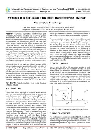
Inverter used for DC to AC conversion, can be of buck inverter,boostinverter,andbuckboostinverter.Thebuck boostinvertercan bederived from the normal buck boost DC-DCconverter and full bridge inverter. Gain ofthe buck boost inverter can be improved by introducinga switched inductorconcepttotheinputinductor.Aswitchedinductor basedbuckboostinverterhasfourworkingmodes.Circuit diagramisshowninfigure1.Circuitconsistsoffivepower switchesS1,S2,S3,S4andS5,fourdiodes,threeinductors,one capacitorC,andaresistiveloadR
Fig -1:Switchedinductorbasedbuckboostinverter
Thecontinuousconductionmode(CCM)ofthebuckboost inverterismainlydividedintofourmodes. Themode1and mode2correspondtothepositivehalfcycleandmode3and mode4correspondtothenegativehalfcyclesoftheoutput voltage.
International Research Journal of Engineering and Technology (IRJET) e-ISSN: 2395-0056
Volume: 09 Issue: 10 | Oct 2022 www.irjet.net p-ISSN: 2395-0072
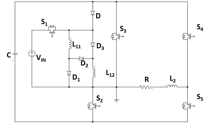
Inthismode,theswitchesS1,S3,andS5 areturnedON.The energy storage inductors L11 and L12 stores energy from source through power switch S1 and capacitor C supplies energytotheloadthroughswitchesS3andS5.Allthecurrent flowingpathscorrespondingtothismodeofoperationare highlightedwiththicklinesasshowninfigure2.
Fig -2:Operatingcircuitof mode1
Inthismodeofoperation,thepowerswitchS5 isturnedON andalltheremainingswitchesareturnedOFF.Theinductors L11 andL12 supplyitsstoredenergytothecapacitorC.The currentintheinductorL2freewheelsthroughswitchS5and antiparallel diode of switch S2. All the conducting paths correspondtothismodeofoperationarehighlightedwith thicklinesasshowninfigure3.
Fig -4:Operatingcircuitof mode3
Duringthismode,thepowerswitchS2 iskeptONwhilethe remainingpowerswitchesareturnedOFF.Inthismode,the inductors L11 and L12 supply its stored energy to the capacitor C. The current in the inductor L2 freewheels throughswitchS2andantiparalleldiodeofswitchS5.Allthe conductingpathscorrespondingtothismodeofoperation arehighlightedwiththicklinesasshowninfigure5.
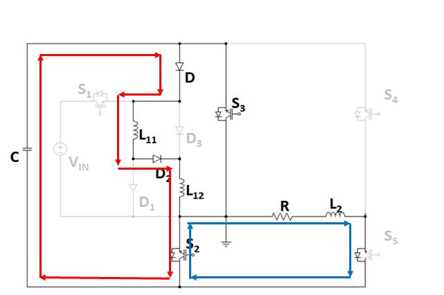
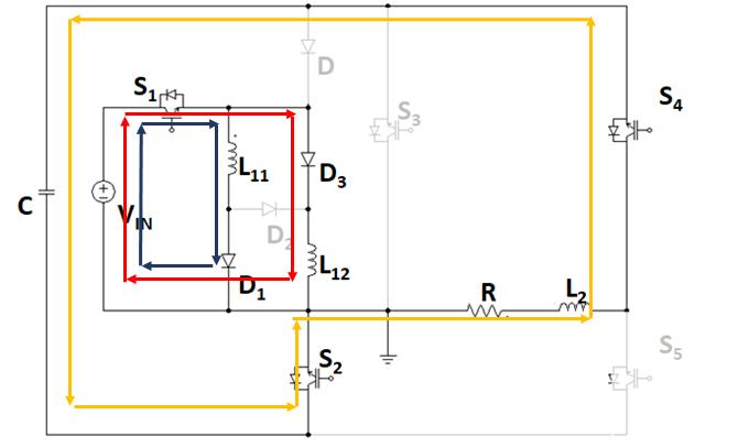
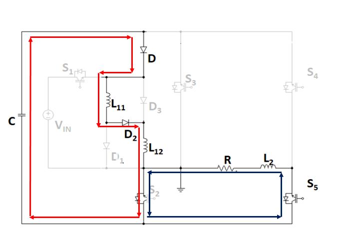
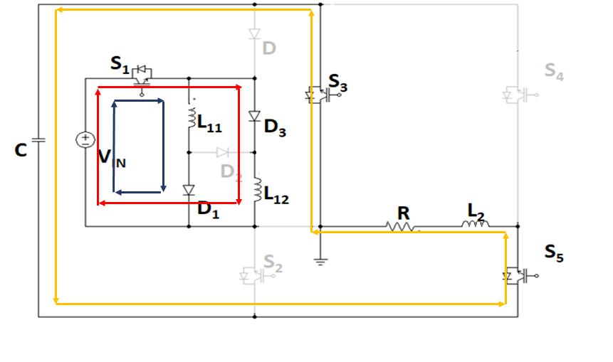
Fig -3:Operatingcircuitof mode2
During this mode, the power switches S1, S2, and S4 are turned ON. The capacitor C supplies energy to the load through power switches S2 and S4. The energy storage inductors L11 and L12 store energy from the input source throughswitchS1.Alltheconductingpathscorrespondingto thismodeofoperationshownareinfigure4.
Fig -5:Operatingcircuitof mode4
TheinputvoltageVIN istakenas75V.Thecomponentsare designed foranoutputvoltageVO of110V.Thepulses are switchedattherateof10kHz.
G= (1)
d=modulationindex
L11=L12 (2)
VoltagerippleratioofcapacitorCislessthan5%of VC
International Research Journal of Engineering and Technology (IRJET) e-ISSN: 2395-0056
Volume: 09 Issue: 10 | Oct 2022 www.irjet.net p-ISSN: 2395-0072
Simulationparametersfortheswitched inductorbasedbuck boost inverter is given in Table 1. The switches are IGBT/Diodewithconstantswitchingfrequencyof10kHz.
Parameters Specification
Inputvoltage(VIN) 28V
Outputvoltage(VO) 110V
Switchingfrequency(fs) 10kHz
Ratedoutputpower(PO) 300W
Outputloadresistance(RO) 40Ω
InductorL11 &L12 70µH
CapacitorC 50µF
The switched inductor based buck boost transformerless inverterissimulatedinMATLAB/SIMULINKbychoosingthe parameterslistedinTable1.Gatepulsegenerationcircuitis showninfigure6
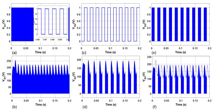
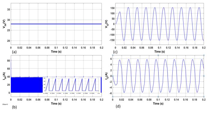
Fig -7:(a)InputvoltageVIN,(b)InputcurrentIIN,(c) OutputvoltageVO and OutputcurrentIO
Figure7showsinputandoutputvoltageandcurrent.Input voltage VIN is 28V and the input current IIN is 19A. Output voltageVO is110VandtheoutputcurrentIO is4.1A.
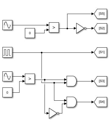
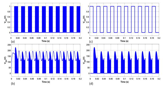
Figure8showsgatepulseandvoltageacrossswitchesS1,S2 and S3. The switching frequency is chosen to be 10kHz. Voltageacrossswitch S1 is225V,voltageacrossswitch S2is 190VandvoltageacrossswitchS3 is190V.
Figure9showsgatepulseandvoltageacrossswitchesS4and S5. Theswitchingfrequencyischosentobe10kHz.Voltage acrossswitchS4is190VandvoltageacrossswitchS5is190V.
Thesimulationresultsoftheswitchedinductorbasedbuck boostinverterisshowninthefollowingfigures.
Fig -8:(a)GatepulsetoS1,(b)VoltageacrossS1 (c)Gate pulsetoS2, (d)VoltageacrossS2,(e) GatepulsetoS3, and (f)VoltageacrossS3
Fig -9:(a)GatepulsetoS4,(b)VoltageacrossS4,(c)Gate pulsetoS5, and(d)VoltageacrossS5
International Research Journal of Engineering and Technology (IRJET) e-ISSN: 2395-0056
Volume: 09 Issue: 10 | Oct 2022 www.irjet.net p-ISSN: 2395-0072
Table 2 shows component wise comparison of different transformerless inverters. Even though switched inductor based buck boost transformer less inverter has more number of components, it has high gain.(SIBBTI-Switched InductorbasedBuckBoostTransformerlessInverter)
Table -2: SampleTableformat
Parameters
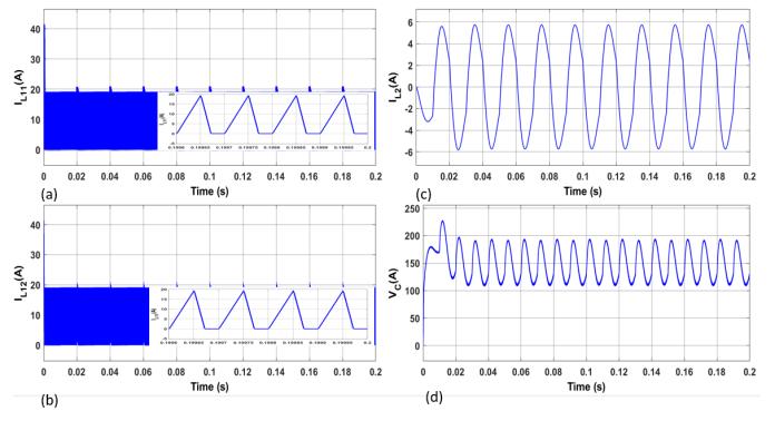
Fig -10:(a)CurrentthroughinductorL11,(b)Current throughinductorL12,(c)CurrentthroughinductorL2 and (d)VoltageacrosscapacitorC
Efficiencyofapowerequipmentisdefinedatanyloadasthe ratioofthepoweroutputtothepowerinput.Theefficiency tellsusthefractionoftheinputpowerdeliveredtotheload. Chart1showsefficiencyVsoutputpowercurveforRload. The inverter efficiency 92% for switched inductor based buckboostinverterforRload.
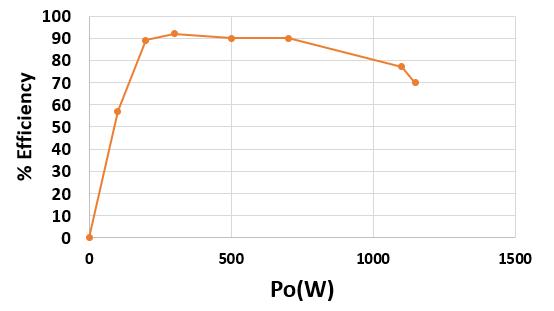
Chart -1:EfficiencyVsOutputPowercurveforRload
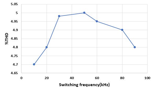
Theplotof %THDoftheinverterasafunctionofswitching frequencyisshowninChart2.MinimumTHDwasobtained at10kHzofswitchingfrequency.
SIBBTI [1] [4] [3]
Noofswitches 5 5 6 5
Noofdiodes 4 1 0 2
Noofinductors 3 2 1 2 Noofcapacitors 1 1 1 0
Totalnoofcomponents 12 9 8 9
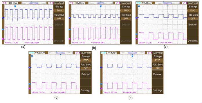
Dspacecontrollerisusedforgeneratingswitchingpulsesfor eachswitch.Thepulsesfrommicrocontrollerwhichisabout 5Visamplified bydrivercircuitthatconsistofTLP250H. Drivercircuitproducespulseof12Vfordrivingtheswitch. The controller output and the driver output is shown in figure11.SwitchesS1,S3 andS4 haveafrequencyof10kHz andotherswitchesS2 andS5 withfrequency50Hz.
Chart -2:%THDVsswitchingfrequency
Fig -11:Pulseforswitch(a)S1,(b)S2,(c)S3,(d)S4,(e)S5
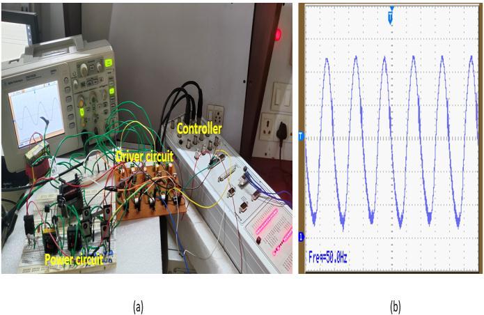
Theoutputof7.6V,50Hzisobtainedfromhardwaresetupas shown in figure 12(a) and output waveform is shown in figure12(b).
International Research Journal of Engineering and Technology (IRJET) e-ISSN: 2395-0056
Volume: 09 Issue: 10 | Oct 2022 www.irjet.net p-ISSN: 2395-0072
IEEE42ndPhotovolt.Spec.Conf.,NewOrleans,LA, USA,Jun.2015,pp.15.
[5] LiYunxia,ZhangQandYuQiao,“Cascadedquasi-Z sourceinverterbasedonswitched-inductor”,IEEE 3rdInternationalElectricalandEnergyConference, vol.32,no.7,2013.
Fig -12:(a)Hardwaresetup,(b)Output
Switched inductor based buck-boost transformerless inverter topology was analyzed and validated through simulationresults.Buckboosttransformerinvertertopology injectszeroleakagecurrentandnegligibleDCcurrentgridconnected PVapplication.Duetothebuck-boost property themaximumpowerpointcanbetrackedforPVunderthe wide voltage variation. The inverter was tested at the switchingfrequencyof10kHzandithasbeenobservedthat switchedinductorconcept improveditsgainandefficiency. Thecontroloftheproposedinverterisimplementedusing dSPACE DS1104. Inverter prototype of 5W provides the expectedperformancewithanoutputvoltageofnearly8V. Theoverallanalysisconfirmsthattheproposedinvertercan beusedinapplicationssuchasphotovoltaics,microgrids, electricvehiclesetc.
[1] Phani Kumar Chamarthi, Mohamed Shawky El Moursi,”A Novel Single-Stage Buck-Boost Transformerless Inverter for 1Ø- Grid-Connected Solar PV Systems”, IEEE Conference on Applied Power Electronics Conference and Exposition (APEC),vol.24,June2020
[2] V. Agarwal and S. Jain , “A single-stage gridconnectedinverter topologyforsolarPVsystems withmaximumpowerpointtracking”,IEEETrans. PowerElectron.,vol.22,no.5,pp.19281940,Sep. 2007.
[3] T. Sreekanth, N. Lakshminarasamma, and M. K. Mishra,”A single-stage grid-connected high gain buck-boost inverter with maximum power point tracking”,IEEETrans.EnergyConvers.,vol.32,no. 1,pp.330339,Mar.2017.
[4] P. Chamarthi, M. Rajeev, and V. Agarwal, “A novel singlestage zero leakage current transformerless inverter for gridconnected PV systems”, in Proc.
value: