International Research Journal of Engineering and Technology (IRJET) e-ISSN:2395-0056

Volume: 09 Issue: 10 | Oct 2022 www.irjet.net p-ISSN:2395-0072
International Research Journal of Engineering and Technology (IRJET) e-ISSN:2395-0056
Volume: 09 Issue: 10 | Oct 2022 www.irjet.net p-ISSN:2395-0072
S
Suma,Dr. Kiran V2
1MTECH 1st year, Dept. of ECE, RV college of Engineering, Karnataka, India
2Associate Professor, Dept. of ECE, RV college of Engineering, Karnataka, India ***
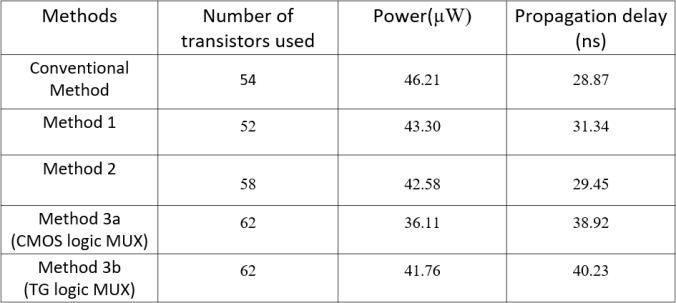
Abstract - With the development of VLSI design, the integrated chip’s gate count is continually increasing, which increases power dissipation and reduces the speed .Therefore, a new architecture that can overcome these limitations needs to be designed. In this paper 1 bit Full Subtractor is designed using various methods and most feasible solution is suggested. The designs have been simulated using Cadence Virtuoso 180nm CMOS technology. Using two XOR gates and 2:1 Multiplexer (MUX) to design a Full Subtractor circuit has turned out to be the most practical design for a full subtractor. It uses 58 transistors uses 42.58uW of power, and propagation delay of 29.45ns making it the most optimized design in comparison to all othermethods.
Key Words: Full Subtractor, Multiplexer, Cadence Virtuoso,CMOStechnology,propagationdelay
AsCMOStechnologyadvancestowardsthenanometer by scaled-down devices. Initially, the main concern for a VLSIdesignengineerwastoreducethecircuitparameters such as area, cost, performance and reliability whereas power consumption was considered next. However, in recentyears,electricityusagehasbeengivenequalweight to all other factors. Low power consumption is a key component in developing the right solution. To lower the heat generated by the circuit, power degeneracy must be reduced.
The most important requirement is to identify the sourceofpowerlossandtakenecessaryactiontoaddress itbyutilizing propermethodologyandtechniquethatcan producethebestresults.
In order to achieve maximum efficiency in terms of transistorcount,delay,andpowerconsumption,theaimis to modify the basic structure of the existing subtractor circuit using a variety of methods, and then come to a conclusionregardingthemosteffectivemethodamongthe mentionedmethods.
Thepaperisorganizedasfollows:SectionIIprovidesa description on the basic structure of a full subtractor.
which aides in recommending the best full subtractor design that has been optimized. Section IV all of the full subtractormethodsmentionedinthepaperarecompared usingtheresultsofvariousdesignpropertiesanalyses.
Subsequently, section V presents the outcome’s conclusion.
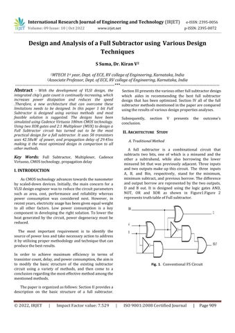
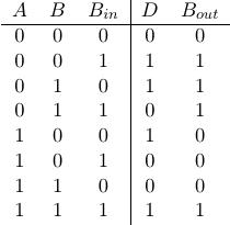
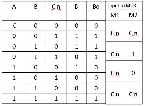
A full subtractor is a combinational circuit that subtracts two bits, one of which is a minuend and the other a subtrahend, while also borrowing the lower minuend bit that was previously adjacent. Three inputs and two outputs make up this circuit. The three inputs A, B, and Bin, respectively, stand for the minimum, minimum subtract, and previous borrow. The difference and output borrow are represented by the two outputs, D and B out. It is designed using the logic gates AND, NOT, OR and XOR as shown in Figure1.Figure 2 representstruthtableofFullsubtractor.
International Research Journal of Engineering and Technology (IRJET) e-ISSN:2395-0056
Volume: 09 Issue: 10 | Oct 2022 www.irjet.net p-ISSN:2395-0072
B. Method 2:Using XNOR Gate and two MUX
Both the difference stage and the borrow step are adjusted inthismethod.Withtheuseoflogicgatesanda 2:1 MUX, the Difference stage is produced. Figure 5 illustrates how the borrow step is realized using a 2:1 MUX.
C. Method 3:Using two 4:1 MUX
Fig-2 :TruthTableof FS
Figure 3 represents input and output waveform of a conventional FS where A, B and C in are the inputs and DifferenceandBorrowaretheoutputs.
To further improve the design, both the difference and the borrow stages have been changed in this method. The difference step in method-2 was implemented using a 4:1 MUX in place of the combination of logic gates and gates in this technique. Using a 4:1 MUX, the borrow stage is implemented. The VEM technique is used to realize this design which is shown in Figure 7 and Figure 6 which shows the logicalstructure of this method.
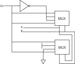
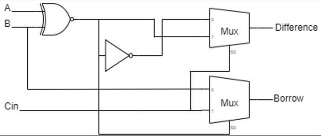
Fig. 3. InputandOutput waveformofFS
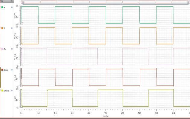
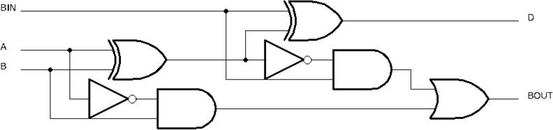
Fig. 4. Method1FS
A. Method 1:Using two XOR gates and a 2:1 MUX
Theborrowstage of this approach substitutes aMulti-
plexer(MUX)withtheANDand ORgates.Asindicatedin Figure 4, the difference stage has been designed using thesametwoXORgatesastheregularFS.
Fig. 5. Method2FS
Fig. 6. Method 3FS
In order to increase the effective size of a k-map Variable Entrant Mapping (VEM) is used and thereby allowing a smaller map to handle a larger number of variables. Therefore, VEM is used to realize the output
International Research Journal of Engineering and Technology (IRJET) e-ISSN:2395-0056
Volume: 09 Issue: 10 | Oct 2022 www.irjet.net p-ISSN:2395-0072
equationsrequiredforthemethod3.AsperFigure7,M1 output variable are the inputs for the first MUX and M2 output variables are the inputs for the second MUX, as showninFigure6.
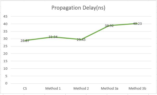
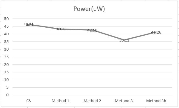
othermethodsthereforemakingitmuchslowerandless efficient. The graphical representation of comparative analysis of all the method with respect to number of transistors, power consumption, and the propagation delayisshowninFigure10,Figure11andFigure12.
The 4:1 MUX is implemented using both CMOS as well as Transmission gate logic. Figure 7 represents 4:1 MUX using Transmission gates where X0,X1,X2,X3 are the inputsand C0,C1aretheselectlinesoftheMUX
Fig. 9. Comparison of allthemethods
This work implements various full subtractor designs and analyses the various design aspects to suggest optimized method. Because less transistors are used in the method 2 FS as compared to all other techniques, it can be concluded that employing two XOR gates and a 2:1MUXwhereMUXisdesignedusingCMOSlogicresults inlowerpowerusage.Therefore, it can be inferred that the most efficient approach to construct an FS that can beintegratedintoasystem’sALUistousetwoXORgates and a 2:1 MUX. The system can be portable and used in energy-efficient applications according to the suggested design.
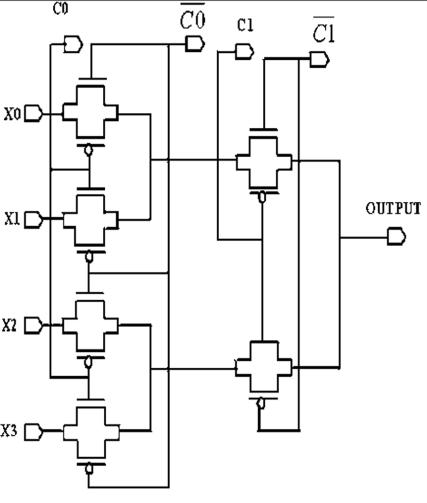
Fig. 8.4:1MUX using TGlogic
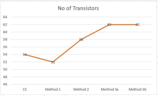
The various Full Subtractor methods is simulated on Cadence Virtuoso tool using 180nm technology with a supply voltage of 1.8V. According to the Comparison Table, the Conventional method has the least propagationdelay(28.87ns) butthepowerconsumedis themostamongstallthemethods(46.21W).TheMethod 1 design is the most optimized since it uses fewer transistors (54) than the other technique. Method 3b utilizesthegreatestnumberoftransistors(62)andhasa higher propagation delay (40.23 ns) compared to all
Fig. 10. TransistorCountComparisonofall themethods
International Research Journal of Engineering and Technology (IRJET) e-ISSN:2395-0056 Volume: 09 Issue: 10 | Oct 2022 www.irjet.net p-ISSN:2395-0072
[4]Y. Gong, M. Luo, C. Wang and T. Yan, ”An MTJ Based 1-Bit Full Subtractor and Its Reading and Writing Circuit,” 2021 IEEE 21st International Conference on Com- munication Technology (ICCT), 2021, pp. 10221025,doi:10.1109/ICCT52962.2021.9658034.
[5]M. T. Emam and L. A. A. Elsayed, ”Reversible Full Adder/Subtractor,” 2010 XIth International Workshop on Symbolic and Numerical Methods, Modeling and Applica-tionstoCircuitDesign(SM2ACD),2010,pp.1-4, doi:10.1109/SM2ACD.2010.5672298.
[6]V.M.Srivastava,S.Kapoor,Nitasha,N.JaswalandG. Singh, ”Full Subtractor Circuit Design with Independent Dou-bleGateTransistor,”2010InternationalConference on Recent Trends in Information, Telecommunication and Computing, 2010, pp. 302-304, doi: 10.1109/ITC.2010.25.
[7]M. Gautam and S. Akashe, ”Reduction of leakage current and power in full subtractor using MTCMOS technique,” 2013 International Conference on Computer Communication and Informatics, 2013, pp. 1-4, doi: 10.1109/ICCCI.2013.6466143.
[8]R.JaiswalandT.N.Sasamal,”Efficientdesignoffull adder and subtractor using 5-input majority gate in QCA,” 2017 Tenth International Conference on Contemporary Com- putting (IC3), 2017, pp. 1-6, doi: 10.1109/IC3.2017.8284336.
[1] M. Sanadhya and D. K. Sharma, ”Design and implementation of full subtractor using different adiabatic tech- niques,” 2020 IEEE International Women in Engineering (WIE) Conference on Electrical and Computer Engineering (WIECON-ECE), 2020, pp. 102106,doi:10.1109/WIECON-ECE52138.2020.9397967.
[2]J. B. Chacko and P. Whig, ”Low Delay Based Full Adder/Subtractor by MIG and COG Reversible Logic Gate,” 2016 8th International Conference on Computational Intelli- gence and Communication Networks (CICN), 2016, pp. 585- 589, doi: 10.1109/CICN.2016.120.
[3]V.G.Nissi,S.MusalaandV.J,”Memristorbasedfull subtractor,” 2022 International Conference on Communication, Computing and Internet of Things (IC3IoT), 2022, pp. 1-5, doi: 10.1109/IC3IOT53935.2022.9767971.
[9] E. V. N. Lakshmi and N. S. S. Reddy, ”Design of reversiblefullsubtractorusingnewreversibleEVNLgate for low power applications,” 2016 International Conference on Inventive Computation Technologies (ICICT), 2016, pp. 1-5, doi: 10.1109/INVENTIVE.2016.7830204.
[10]M.MahaboobBasha,K.VenkataRamanaiahandP. Ramana Reddy, ”Notice of Removal: Novel Energy Efficient one bit Full Subtractor at 65nm technology,” 2015 International Conference on Electrical, Electronics, Signals, Communication and Optimization (EESCO), 2015, pp. 1-5, doi: 10.1109/EESCO.2015.7253873. [11]K. Dhar, A. Chatterjee and S. Chatterjee, ”Design of an energy efficient, high speed, low power full subtractor using GDI technique,” Proceedings of the 2014 IEEE Students’ Technology Symposium, 2014, pp. 199-204, doi:10.1109/TechSym.2014.6808046.
International Research Journal of Engineering and Technology (IRJET) e-ISSN:2395-0056 Volume: 09 Issue: 10 | Oct 2022 www.irjet.net p-ISSN:2395-0072