International Research Journal of Engineering and Technology (IRJET) e-ISSN: 2395-0056
Volume: 9 Issue: 10 | Oct 2022 www.irjet.net p-ISSN: 2395-0072
International Research Journal of Engineering and Technology (IRJET) e-ISSN: 2395-0056
Volume: 9 Issue: 10 | Oct 2022 www.irjet.net p-ISSN: 2395-0072
1MTech Scholar, Department of Electrical and Electronics Engineering, MVGR College of Engineering, Vizianagaram, Andhra Pradesh, India
2Associate Professor, Department of Electrical and Electronics Engineering, MVGR College of Engineering, Vizianagaram, Andhra Pradesh, India ***
Abstract - Inthisarticle,anovelself-balancingswitched capacitor multilevel inverter structure with six-fold gain factorisproposed.Thisinverter'sdesigncallsforasingleDC supply,3capacitors,and14switchestogenerateanoutput voltagewith13levels.Thepowerstoragemechanismused by this inverter construction allows it to automatically balance itself by charging and discharging capacitors in seriesandparallelwithaDCsource.Theproposedinverter doesnotrequireaback-endH-bridge,thereforeeachswitch isnotsubjectedtoasmuchvoltagestressasunderapeak load. The result is a striking reduction in Total Blocking Voltage(TBV)from88Vdc to33Vdc andMaximumBlocking Voltage(MBV)from6Vdc to4Vdc forsimilartopologiesand thus makes it a preferable choice for renewable energy applications. The proposed SBSCI topology modes of operation, capacitor design and control strategy are delineated.Athoroughcomparisonwithexistingliterature demonstrates the proposed topology's affordability and compactness.Theperformanceandviabilityofthesuggested topology are validated using the MATLAB/SIMULINK software.
Words: Maximum Blocking Voltage (MBV), SelfBalancing Mechanism, Total Cost Function (TCF), Voltage gain, Self-Balancing Switched Capacitor Inverter (SBSCI).
Duetotheirbetterwaveformnatureandreducedswitching voltagestressofeachpowerswitch,multileveldc-acpower converters are currently the most widely used solution in industriesforhigh-powerapplicationswithmediumvoltage levels.Itsignificantlybenefitsapplicationsrequiringmedium voltageandhighpower,suchasthoseforelectricvehicles and renewable energy sources. [1],[2]. MLIs have gained popularity because to their intrinsic advantages, which include lowering switching frequency, lowering switching stress, and improving voltage and current waveforms by decreasingharmonics[3].Researchersfromallaroundthe world are paying close attention to the neutral point clamped(NPC),flyingcapacitor(FC),andcascadedH-bridge (CHB)inverters,whichhavealreadyachievedcommercial viability[4].AlthoughtheMLIsbeingadvantageousitalso
sufferswithsomeflawslikecapacitorsbalancingissuesand requirementofcomplexcircuitsincaseofflyingcapacitor inverter(FC)andNeutralpointclampedinverter(NPC).The cascadedH-bridgeinverter(CHB)necessitatesnumerousDC supply’s,increasingthesystem'ssizeandcost.Allofthese conventional MLIs have one thing in common: they aren't capable of raising voltage. To address this issue for the researchers, switching capacitors are the best option. The switchingcapacitortopology-basedMLIhasbecomemore prevalentinrecentyears[5]
Upuntilthispoint,differentswitchedcapacitortopologies have mainly been used in single-phase systems, with the most popular variety being created by stacking switched capacitor topologies with an inverting H-bridge. The ac outputvoltageisproducedbytheH-bridgeontheendside, while the circuit on the front side produces a range of dc levels.Atraditionalseries/parallelswitchingcapacitordc/dc multilevelcircuit,aswellasitsstreamlinedvariantandan updatedstructure,areemployedtopowertheH-bridge[9]. When an H-bridge is used, the switches are under more voltage stress. By using a different commonly utilized integrated circuit created by sandwiching a switching capacitor based multilevel converter circuit between two halfbridges,itispossibletogetbeyondtherestrictionsof thesetopologies[6-8].In[10],amodularswitchedcapacitor topologywasanalyzedwhilekeepingall ofthebenefits of switchedcapacitortopologies.Although[9-10]usessingledc sourcetoattain13-levelsattheoutputbutitprovideswith high switching stress across the switches that limits the topology to work for low power applications. Some topologies suffer with the least gain. However, some topologiesthataimtoincreasehighvoltagelevelsareunable to reduce switching stress [10]. Some switched capacitor topologies requires auxiliary H-bridge for polarity generation [11]. The single source topology requires complexalgorithmsandvoltagebalancingauxiliarycircuits in order to attain high power density. This causes the system's size and cost to grow. The literature analysis mentionedaboveprovidesroomtodevelopanoveltopology thatpossessesthe following appealingqualities.AnSBSCI topologywith13levelsandasix-foldgainfactorisdescribed inthisarticle.
© 2022, IRJET | Impact Factor value: 7.529 | ISO 9001:2008 Certified Journal | Page735
 Key
Key
International Research Journal of Engineering and Technology (IRJET) e-ISSN: 2395-0056
Volume: 9 Issue: 10 | Oct 2022 www.irjet.net p-ISSN: 2395-0072
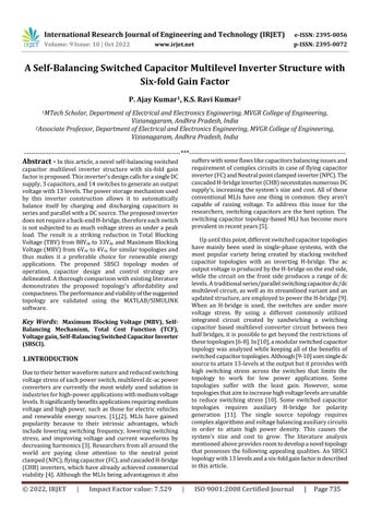
switches,S9istheonlyonethatisbidirectional.Theswitches maximumblockingvoltageislesserthantheloadmaximum voltage.Andthesuggesteddesignthecapacitorsgetcharged anddischargedintheratioof .A batteryoranyotherrenewableenergysourcecouldserveas theintendedtopologyDCpowersource.Switchingpairsthat are complementary to one another include (S2S3), (S8S10), (S11S12),and(S13S14).
Someofthethingsthatmakeituniqueincludethefollowing:
Voltages in a capacitor have a self-balancing tendency.
Maximum Blocking Voltage across each switch is lessthatpeakloadvoltage
It employs 14 switches and three capacitors in a 1:2:2ratiostogenerateanoutputvoltagewaveform with13levels.
Ithasthecapacitytoincreasetheinputvoltage.
The suggested structure responds to dynamic variationsinloadverywell.
This architecture's decreased switching stress makesitappropriateformediumandhighpower applications.
The arrangement of this document is as follows: the secondsegmentdescribesthetopologyarchitectureandits operation.Themodulationschemeandcapacitanceanalysis areshowninSegment3.Thecomparisonofthesuggested designwiththeexistingdesignsisevaluatedinsegment4. Segment 5 displays the findings of the planned topology validationandfollowedbyconclusioninSegment6.
Theproposedinnovativetopologyschematicdiagramalong with maximum blocking voltage along each switch can be seenin Fig1.Itconsists of3 capacitors(C1,C2,andC3), 14 switches (S1–S14), and a single DC source ( ). Out of 14
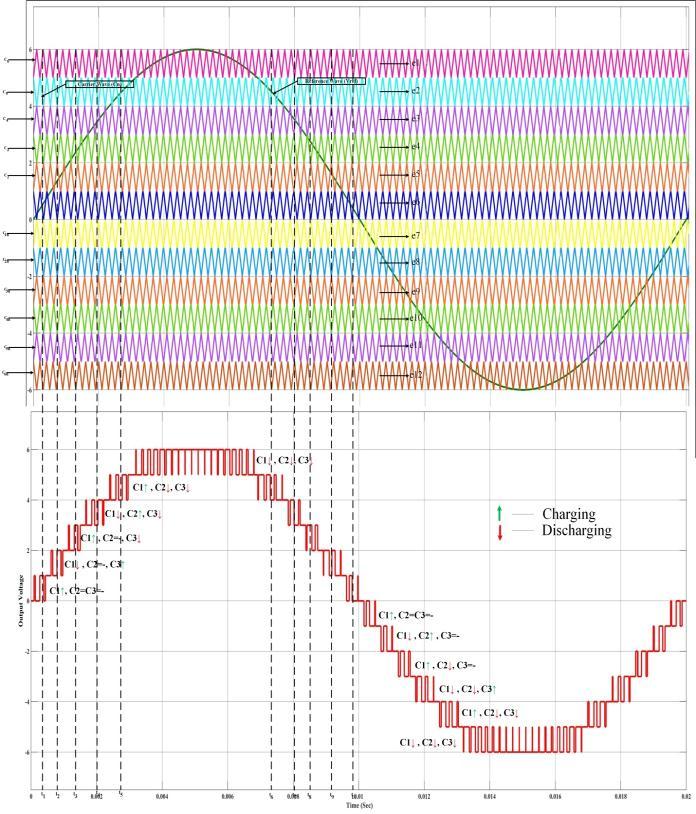
By assuming that each element in the suggested switched capacitorarchitectureisperfect,theanalysisthatfollowsis made simpler. As shown in Tab1 and Fig2, the proposed topologyoperationmaybeexplainedbythirteenstateswith distinct switching sequence that results in 13 levels at output.Tab1containsalistofthesuggestedtopology'slegal switchingcombinations.InTab1,theonandoffstatesofthe switches are indicated by "0" and "1," respectively. The symbolsforthecapacitor'scharging,discharging,andidle statesare↑,↓,−.
State1.
The output voltage can be achieved by activating switches S5, S10, S12, S14. Here Capacitor C1=C2=C3 remains idle(-).ItshownintheFig2(G).
State2.
Theoutputvoltage canbeachievedbyactivating switchesS1,S3,S4,S8,S11,S14 forpositivelevelandshownin Fig2(F) and capacitor C1 gets charged. And by activating switchesS1,S3,S5,S10,S12,S13fornegativelevelandshownin Fig2(H)andcapacitorC1 getscharged.
State3.
Theoutputvoltage canbeachievedbyactivating switches S2, S4, S5, S7, S8, S9, S11, S14 for positive level and shown in Fig2(E) and capacitor C3 gets charged and capacitorC1 getsdischarged.AndbyactivatingswitchesS2, S4, S5, S6, S9, S10, S12, S13 for negative level and shown in Fig2(I)andcapacitorC1getsdischargedandC2getscharged.
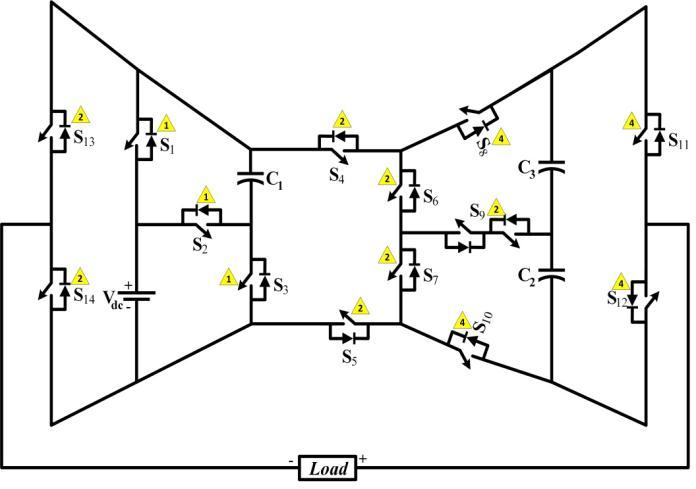
State4.
Theoutputvoltage canbeachievedbyactivating switchesS1,S3,S4,S6,S9,S11,S14 forpositivelevelandshown
International Research Journal of Engineering and Technology (IRJET) e-ISSN: 2395-0056
Volume: 9 Issue: 10 | Oct 2022 www.irjet.net p-ISSN: 2395-0072
Fig2: PositiveandNegativehalf-cycleoperatingstatesalongwithzerostate inFig2(D)andcapacitorC3getsdischargedandcapacitorC1 getscharged.AndbyactivatingswitchesS1,S3,S5,S7,S9,S12, S13 fornegativelevelandshowninFig2(J)andcapacitorC2 getsdischargedandC1 getscharged. State5.
Theoutputvoltage canbeachievedbyactivating switches S2, S4, S5, S6, S9, S10, S11, S14 for positive level and shown inFig2(C)andcapacitorC1 ,C3 gets dischargedand capacitorC2 getscharged.AndbyactivatingswitchesS2,S4, S5,S7,S8,S9,S12,S13 fornegativelevelandshowninFig2(K) andcapacitorC1,C2 getsdischargedandC3 getscharged. State6.
Theoutputvoltage canbeachievedbyactivating switches S1, S3, S4, S6, S7, S10, S11, S14 for positive level and showninFig2(B)andcapacitorC2 ,C3 getsdischargedand capacitorC1 getscharged.AndbyactivatingswitchesS1,S3, S5,S6,S7,S8,S12,S13 fornegativelevelandshowninFig2(L) andcapacitorC2,C3 getsdischargedandC1 getscharged.
State7.
Theoutputvoltage canbeachievedbyactivating switchesS2,S4,S6,S7,S10,S11,S14forpositivelevelandshown inFig2(A)andcapacitorC1 ,C2 ,C3 getsdischarged.And by activatingswitchesS2,S5,S6,S7,S8,S12,S13 fornegativelevel
and shown in Fig2(M) and capacitor C1 ,C2, C3 gets discharged.
Thissubsectiondemonstratestheself-balancingmechanism ofvoltageacrossthecapacitors.Themostcrucialcomponent ofthesuggestedswitchingcapacitorarchitectureisthetrio ofthecapacitorsC1,C2,andC3,whichchargewhenarranged in parallel to the input supply. During the voltage level , , thecapacitorC1 getschargedto During the voltage level C2 , and charges to andduringvoltagelevel , thecapacitorC3 chargesto .ItisenlistedinTab1anddepictedinFig2. ThecapacitorC1getsarrangedinserieswithsourcevoltage toprovidevoltagelevelof , , .Atthesame time the capacitor C2 gets discharged to produce voltage level of , , . And the capacitor C3 gets discharged to produce voltage level of , , .Thecapacitorsnaturallyachieveselfbalanceusingtheseries/parallelapproachofchargingand dischargingthem.
Designingaswitchedcapacitormultilevelinverterrequires carefulconsiderationofthecapacitors'capacitance.Because theeffectivenessoftheinverterisimpactedbythevoltage fluctuationsinthecapacitor.Losseswillincreaseifthe
International Research Journal of Engineering and Technology (IRJET) e-ISSN: 2395-0056
Volume: 9 Issue: 10 | Oct 2022 www.irjet.net p-ISSN: 2395-0072
Tab1: Proposed13SBSCITopologyswitchingstates
Switching States
Switches
Charging & Discharging of Capacitors
S1 S2 S3 S4 S5 S6 S7 S8 S9 S10 S11 S12 S13 S14 C1 C2 C3
+6Vdc 0 1 0 1 0 1 1 0 0 1 1 0 0 1 ↓ ↓ ↓
+5Vdc 1 0 1 1 0 1 1 0 0 1 1 0 0 1 ↑ ↓ ↓
+4Vdc 0 1 0 1 1 1 0 0 1 1 1 0 0 1 ↓ ↑ ↓
+3Vdc 1 0 1 1 0 1 0 0 1 0 1 0 0 1 ↑ ↓
+2Vdc 0 1 0 1 1 0 1 1 1 0 1 0 0 1 ↓ ↑
+1Vdc 1 0 1 1 0 0 0 1 0 0 1 0 0 1 ↑
0 0 0 0 0 1 0 0 0 0 1 0 0 0 1
-1Vdc 1 0 1 0 1 0 0 0 0 1 0 1 1 0 ↑
-2Vdc 0 1 0 1 1 1 0 0 1 1 0 1 1 0 ↓ ↑
-3Vdc 1 0 1 0 1 0 1 0 1 0 0 1 1 0 ↑ ↓
-4Vdc 0 1 0 1 1 0 1 1 1 0 0 1 1 0 ↓ ↓ ↑
-5Vdc 1 0 1 0 1 1 1 1 0 0 0 1 1 0 ↑ ↓ ↓
-6Vdc 0 1 0 0 1 1 1 1 0 0 0 1 1 0 ↓ ↓ ↓
capacitor's voltage ripple is greater, and vice versa. The maximumdischargingduration,maximumloadcurrent,and power factor angle are additional elements that affect a capacitor'sdischargevalues.Consequently,thedischarging quantity( )ofthecapacitorisshownas
equation1
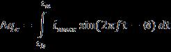
Where representsthehighestloadcurrent,betweenthe loadvoltageandcurrent,thereisapowerfactorangle(ɸ), thelowerandupperboundsofeachcapacitor'sdischarging durationare(ta-tb),“f”indicatesthefundamentalfrequency, ɸ be the power factor angle between and , the longestdischargingperiodofthecapacitorsC1,C2,andC3are .
Fig3 StatesofcharginganddischargingofCapacitors alongwithmodulationschemefor13SBSCItopology
International Research Journal of Engineering and Technology (IRJET) e-ISSN: 2395-0056
Volume: 9 Issue: 10 | Oct 2022 www.irjet.net p-ISSN: 2395-0072
Forthesuggested13-leveltopologyt1,t2,t3,t4,t5,t6,t7,t8,t9,t10 areevaluatedwithhelpofFig3asfollows: , , , , , , , , ,
equation5
equation2
If percentageisthehighestpermittedvoltageripple,the idealcapacitanceisgivenby equation3
The ideal capacitance value under the resistive load (RL) conditioncanbestatedas equation4
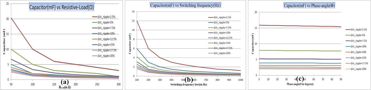
It is obvious from equation (4) that the percentage of capacitor voltage ripple ( ) for resistive loads (RL) is inversely proportional to the magnitude of the ideal capacitor.Inordertothesizeofcapacitorwillreducesasany oneofthesefactorsincreasesanditisdepictedinFig4(a)(b).
Foraninductiveload(RL),theidealcapacitancevaluecanbe statedas
Itisobviousfromequation(5)thatthecapacitancevalueof aninductiveloadisproportionaltophaseangledepictedin theFig4(c).Byincreasingthevalueofcapacitancethephase angle gets increases. Therefore power factor, switching frequency,andloadresistanceshouldbeselectedinsucha way that the value of capacitance is selected. Therefore capacitor ripples should be in permissible limit. For the proposed topology the capacitor values are C1=3300μf, C2=C3=4700μf.
There are numerous control mechanisms utilized for multilevel inverters. In this article, a straightforward multicarrier level-shifted PWM has been employed. By comparing the signals from 12 carriers (Cn) (e1, e2,.....e12) with a sinusoidal signal (Vref)., the switching pulse is determined.Eachcarrier'samplitudeandfrequencyhavethe same peak to peak value. The modulation scheme for the proposed13SBSCIisdepictedintheFig3.
Capacitors( ),diodes( ),drivers( ), gain, maximum blocking voltage (MBV), switches, total standing voltage (TSV), and Total cost function (TCF) are compared to highlight the significance of the suggested 13SBSCI design. The findings of the comparison studies between the suggested 13SBSCI design and the existing topologiesaredisplayedinTAB2. Thecomparisonsusedto assess the benefits of the suggested 13SBSCItopology primarily took into account the boosting ability, Total standingvoltage(TSV),MaximumBlockingVoltage(MBV), andTotalcostfunction(TCF).TheTotalStandingVoltage
International Research Journal of Engineering and Technology (IRJET) e-ISSN: 2395-0056
Volume: 9 Issue: 10 | Oct 2022 www.irjet.net p-ISSN: 2395-0072
Reference Gain(G) TSV MBV Cost Function
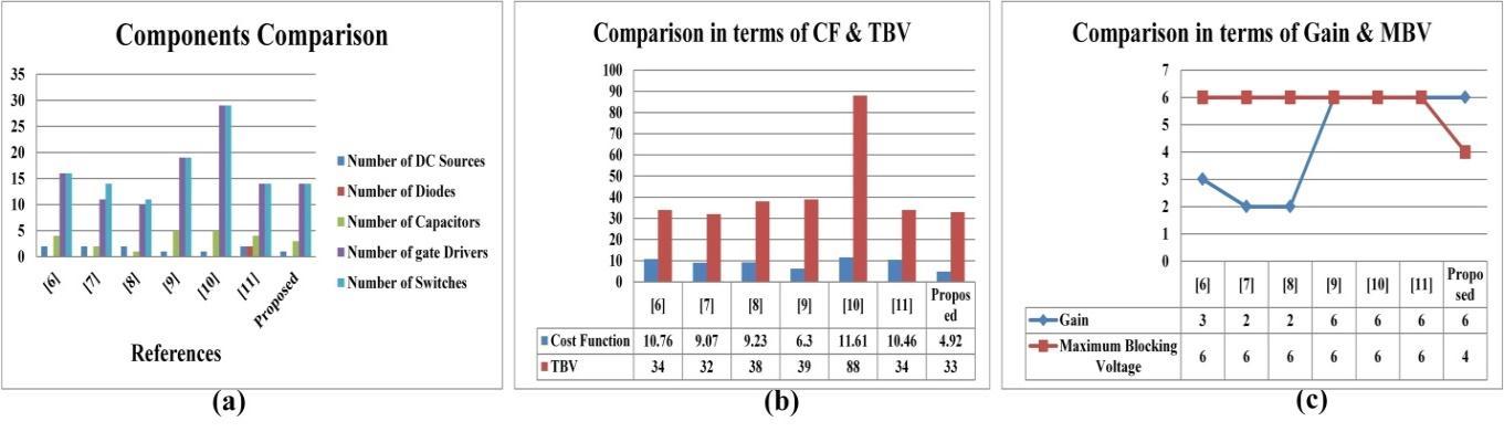
[6] 16 0 4 16 2 3 34 13 6 10.76
[7] 14 0 2 11 2 2 32 13 6 9.07
[8] 11 0 1 10 2 2 38 13 6 9.23
[9] 19 0 5 19 1 6 39 13 6 6.30
[10] 29 0 5 29 1 6 88 13 6 11.61
[11] 14 2 4 14 2 6 34 13 6 10.46
Proposed 14 0 3 14 1 6 33 13 4 4.92
(TSV) can be calculated as the summation of maximum voltagestressacrosstheeachindividualswitches.Thecost function(CF)ofaninverterisdescribedas:
equation 6
The weight factor, which is equal to the importance of switchingcomponents,isdenotedbythesymbol( .TAB2 comparesswitchedcapacitortopologieswithvariousvoltage gains at the same voltage levels. The design cost of the invertersisincreasedbythetopology[10]’sextensiveuseof semiconductor components, which also raises the overall standing voltage. On the other hand, there are fewer switchesinthetopologies[7][8]thatareputundermore strainthanthesourcevoltage.Tooffsettheoutputvoltage risebyafactorofsix,thetotalcostfunction(TCF)ishigh.
Thisisanimportantfactortotakeintoaccountbecausethe Maximumblockingvoltageoftheswitchissixtimeslargerin [6-11] designs. The required voltage level, according to [9][10],canonlybereachedemployingseveralcapacitorsin itsconstruction.Thedesigndescribedin[11]usesseveral diodes, which raises count of semiconductors usage and raiseslosses,whichisanotherimportantconcern. Insome topologies[6-11]themaximumblockingvoltage(MBV)is highwhichlimitstolowpowerapplications.Fig5depictsthe comparison assessment of 13SBSCI topology with current literatureintermsofcomponentcountinFig5(a),Totalcost function (TCF) and TBV in Fig5(b), and gain &MBV in Fig5(c).
Using the values listed in TAB3, MATLAB/Simulink tools havebeenutilizedtosimulatetheproposed13SBSCIdesign. In dynamic conditions, the proposed switching capacitor topologywastested.Inductive-resistiveloadconfiguration outputwaveformisshowninFig.6.
Fig5 ComparativeAssessmentof13SBSCItopologywithcurrentliteratures
International Research Journal of Engineering and Technology (IRJET) e-ISSN: 2395-0056
Volume: 9 Issue: 10 | Oct 2022 www.irjet.net p-ISSN: 2395-0072
Parameters Specification
Sourcevoltage 40V
Switching-Frequency 2500Hz,5000Hz
RLLoad(R0+RL) 40Ω+50mH,40Ω,40Ω+150mH
Fundamentalfrequencyfo 50Hz
CapacitorsC1 ,C2 ,C3 3300uF,4700uF,4700uF
PowerSwitches IGBT
Voltage ripple( ) 5%
Itisdiscoveredthattheloadvoltageissixtimesmorethan thesupplyvoltagewhenitreachesitsmaximum. Andthe waveformoftheoutputvoltageinFig6illustratesthatthe designisattachedataload40Ω+50mH.Inthiswaveformthe capacitorC1chargesto40Vassourcevoltageandcapacitors C2,C3 chargesto80Vfromwherenaturalvoltagebalancing processwilloccursundersteadystate.
Fig7 waveformofproposed13SBSCItopologyunder changeinModulationIndex
Fig.7illustratesdesignedtopologycanfunctionwitharange ofM.Ivalues (1,0.75,and0.50).This enables the planned inverter to have a different number of output levels. Furthermore,inreactiontoshiftingM.I.values,theoutput waveformandamplitudechange.Therearethirteenoutput levelsinitially,theneleven,andfinallyseven.Asaresult,the proposedSBSCItopologyworksappreciablyforvariousM.Is. Fig8depictsthedesignedtopologytotalharmonicdistortion (THD) percentage in current and voltage outputs under variouslevelshiftcontrolscheme.
Fig6 Waveformofoutputvoltageandcurrentunder steadystateconditionalongwithcapacitorvoltages
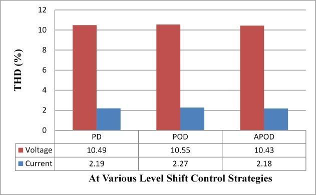
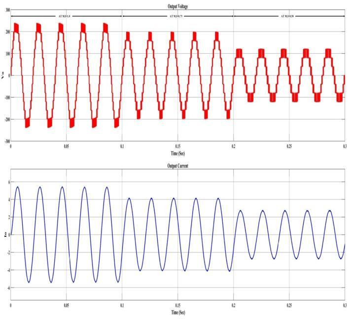
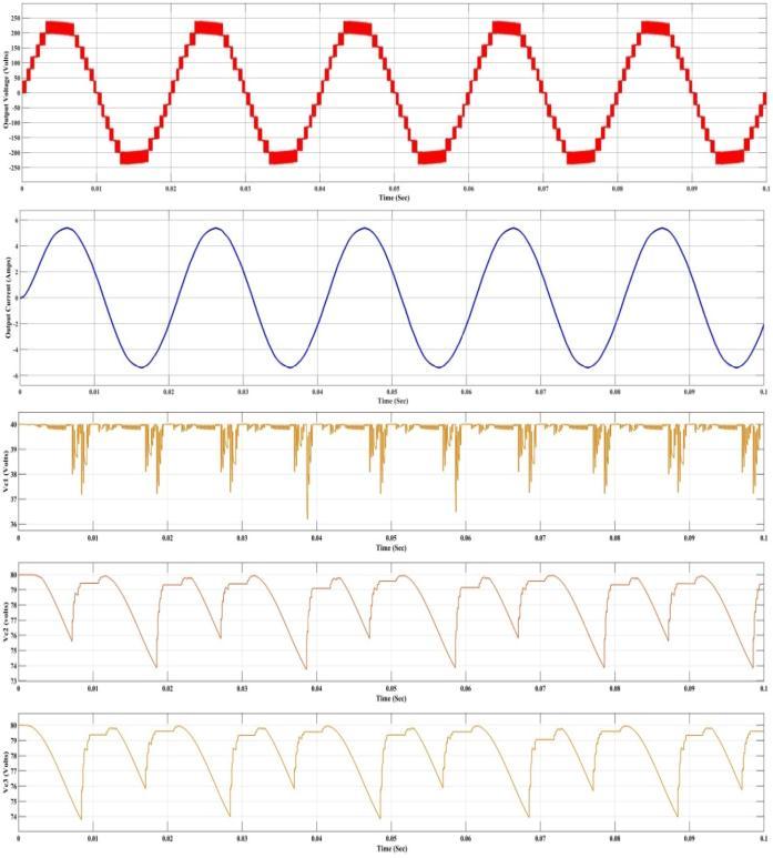
Fig8 ProposedtopologyTHD(%)forvariouslevelshift controlscheme
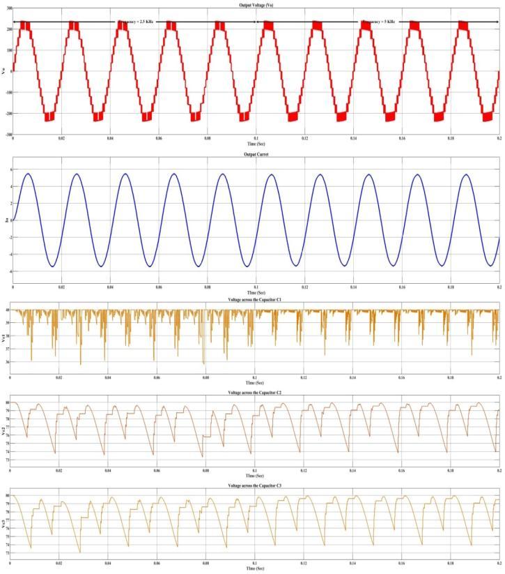
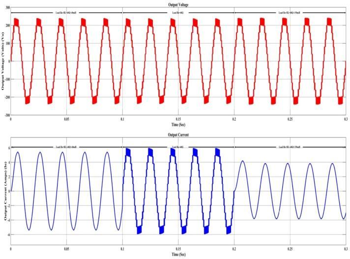
Fig.9showshowtheintendedarchitecturecanfunctionwith changingintheload.Therehavebeenreportsthatthe13level is generated by the suggested 13SBSCI architecture with a six-fold increase in step potential from the input voltage. Here system is first operated with 40Ω+50mH, second it is operated at 40Ω, and third it is operated at 40Ω+150mH.Asaresult,theproposed13SBSCIworkswell for step change in load. From Fig10 it illustrates that the designedtopologyworkabilityunderfrequencyvariationof
International Research Journal of Engineering and Technology (IRJET) e-ISSN: 2395-0056
2500 Hz for 5 cycles and 5000 Hz for next 5 cycles with outputvoltage,currentandtriocapacitorsoutputvoltage.
Fig9 Proposedtopologyworkabilityunderstepchangein load
Thetopologydiscussedinthisstudyisalowswitch-count, boost-capable, self-voltage-balanced 13-level SBSCI topology.Thesuggestedarchitectureusesonly14switches togeneratethirteenlevelsandbooststheoutputto6times from one DC supply. When compared to other switched capacitor topologies that have been previously published, the proposed topology displays a lower TSV and MBV. A detailedinvestigationofperformancecomparisonsshowed thattheproposedswitchedcapacitortopologyoutperforms comparable prior-art. The enhanced voltage boosting capabilitiesalsomakesthetopologysuitableforrenewable energyapplications.Theresultsofthesimulationconfirmed the circuit's functionality and showed voltage boosting capabilityforwiderangeofM.Is,goodvoltageandcurrent regulation for load and frequency variation, and reduced switchingstress.Theproposedswitchedcapacitortopology offers strong structural and functional benefits for high voltageapplications
Fig10 Frequencychangeform2500Hzto5000Hzof proposed13SBSCItopology
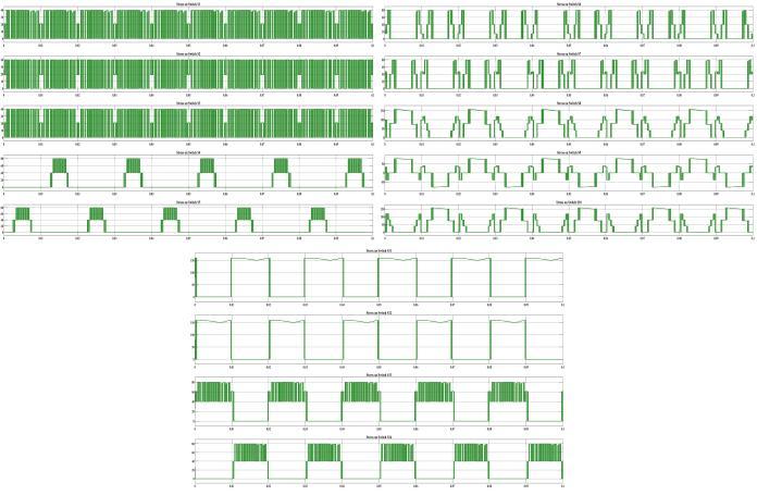
FromFig11itdepictsthattheswitchingstressvoltageacross each switched used in designed 13SBSCI topology. The maximumblockingvoltageinproposedSBSCIstructure is justfourtimesthesourcevoltage.Theproposedarchitecture can therefore be used in high power applications. The aforementioned scenarios demonstrate the suggested switchedcapacitortopology'ssuperiorresponsiveness.
Volume: 9 Issue: 10 | Oct 2022 www.irjet.net p-ISSN: 2395-0072 © 2022, IRJET | Impact Factor value: 7.529 | ISO 9001:2008 Certified Journal | Page742
[1] P. R. Bana, K. P. Panda, R. T. Naayagi, P. Siano, and G. Panda,‘‘Recentlydeveloped reducedswitchmultilevel inverter for renewable energy integration and drives application: Topologies, comprehensive analysis and comparativeevaluation,’’ IEEE Access,vol.7,pp.54888–54909,2019.
[2] B.P.Reddy,M.A.Rao,M.Sahoo,andS.Keerthipati,‘‘A fault-tolerant multilevel inverter for improving the performance of a pole–phase modulated nine-phase induction motor drive,’’ IEEE Trans. Ind. Electron.,vol. 65,no.2,pp.1107–1116,Feb.2018.
[3] J. S. M. Ali and V. Krishnaswamy, ‘‘An assessment of recent multi-level inverter topologies with reduced power electronics components for renewable
International Research Journal of Engineering and Technology (IRJET) e-ISSN: 2395-0056
applications,’’ Renew. Sustain. Energy Rev., vol. 82, no. 3,pp.3379–3399,Feb.2018.
[4] M.Vijeh,M.Rezanejad,E.Samadaei,andK.Bertilsson,“A general review of multilevel inverters based on main sub-modules: Structural point of view,” in IEEE TransactionsonPowerElectronics,vol.34,no.10,pp. 9479–9502,Oct.2019.
[5] Jena,Kasinath,ChinmoyKumarPanigrahi,andKrishna Kumar Gupta. "A 6X-Voltage-Gain 13-Level Inverter With Self-Balanced Switched-Capacitors." CPSS Transactions on Power Electronics and Applications 7,no. 1,pp.94-102,2022
[6] T. Roy, P. K. Sadhu, and A. Dasgupta, “Cross-Switched Multilevel Inverter Using Novel Switched Capacitor Converters,” IEEE Trans. Ind. Electron.,vol.66,no.11,pp. 8521–8532,Nov.2019.
[7] E.Samadaei,M.Kaviani,andK.Bertilsson,“A13-levels Module( K-Type)withtwo DCsourcesforMultilevel Inverters,” IEEE Trans. Ind. Electron., vol. 66, no. 7, pp.5186-5196,2018.
[8] M.D.Siddique,S.Mekhilef,A.Sarwar,A.Alam,andN.M. Shah, “Dual asymmetrical dc voltage source based switchedcapacitorboostmultilevelinvertertopology,” IET Power Electron.,vol.13,no.7,pp.1481–1486,2020.
[9] Y. Hinago and H. Koizumi, “A switched-capacitor inverterusingseries/parallelconversionwithinductive load,” IEEE Trans. Ind. Electron.,vol.59,no.2,pp.878–887,Feb.2012.
[10] A.Taghvaie,J.Adabi,andM.Rezanejad,“ASelf-Balanced Step-Up Multilevel Inverter Based on SwitchedCapacitor Structure,” IEEE Trans. Power Electron., vol. 33,no.1,pp.199–209,Jan2018.
[11] T.RoyandP.K.Sadhu,“AStep-UpMultilevel Inverter Topology Using Novel Switched Capacitor Converters withReducedComponents,” IEEE Trans. Ind. Electron., vol.68,no.1,pp.236–247,Jan.2021.
“P.AjayKumarhasreceived his Bachelor of Technology degree in Electrical & ElectronicsEngineeringfrom MVGRCollegeofEngineering, Indiain2020.Heiscurrently pursuingfinalyearinMaster of Technology in the specialization of Power Systems, MVGR College of Engineering, Andhra Pradesh,India.”
“K S RAVI KUMAR (M’20) wasborninKharagpurIndia onApril18,1977.Hedidhis B. Tech degree in Electrical engineering in SVHCE, Nagarajuna University, Machilipatnam,A.P,India,in 1999,didhisM.Techdegree incontrolsystemsfromNIT Kurukshetra in 2002. Presently he is pursuing his PhD in Electrical Engineering, at KL University,Guntur,A.P.,India since 2015. He is also workinginMVGR College of engineering, Vizianagaram, A.P., India since 2002, presently as Associate Professor. His Research Interests are in the area of Bidirectional DC-DC Converters in Power Electronics,ElectricVehicles, Embedded Controllers and Artificial Intelligence. Mr.Kalamchety was a member of IET since 2017. HeisalsoamemberofIEEE. He has around 8 InternationalJournalsand19 International Conference Publications and 3 Indian patents published to his credit.”
Volume: 9 Issue: 10 | Oct 2022 www.irjet.net p-ISSN: 2395-0072 © 2022, IRJET | Impact Factor value: 7.529 | ISO 9001:2008 Certified Journal | Page743