International Research Journal of Engineering and Technology (IRJET)
e-ISSN: 2395-0056
Volume: 07 Issue: 01 | Jan 2020
p-ISSN: 2395-0072
www.irjet.net
A Survey on Reconstruct Structural Design of FPGA Rohit Raj1, Navneet Singh2 1,2Assistant Professor, Gurdasidevi Institute of Management & Technology, Budhlada- India
---------------------------------------------------------------------***----------------------------------------------------------------------
Abstract - The digital circuit for eternity has been to a great extent subjective by new types of Field Programmable devices which are having complicated architectures e.g. FPGAs and CPLDs, in the current years. This paper is for evaluating those architectures in conditions of area and speed concert. Key Words: FPGA, Look-Up Table (LUTs), Xilinx, CAD Tools, Configurable Logic Block (CLB) 1. INTRODUCTION Today's the biggest Coordinated Circuits into the business sectors are amazingly complex field- programmable gate array items (FPGA). For instance, the Xilinx, Altera has created the programmable gadgets around 10 million transistors in 0.5-micron advances and measures about 1.8 cm l.5 cms. These outcomes are because of the advances in amazingly explore and improvement both in scholastics and businesses. The aggregate investigation of at present accessible and quantities of the most industrial gadgets of field-programmable gadgets are outlined in an ongoing article in IEEE Plan and Trial of PCs. In this paper I am attempting to depict, assessing the improvement in engineering of FPGA that impact the absolute chip zone and execution of speed. With the assistance of research contemplates I will attempt to keep the steady highlights utilized for business items.
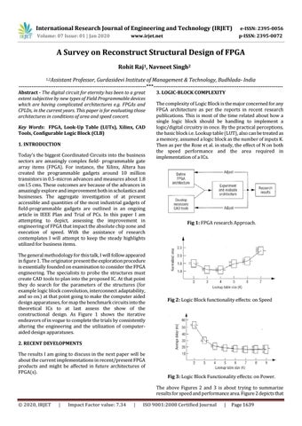
The general methodology for this talk, I will follow appeared in figure 1. The originator present the exploration procedure is essentially founded on examination to consider the FPGA engineering. The specialists to probe the structures must create CAD tools to plan into the proposed IC. At that point they do search for the parameters of the structures (for example logic block convolution, interconnect adaptability, and so on.) at that point going to make the computer aided design apparatuses, for map the benchmark circuits into the theoretical ICs to at last assess the show of the constructional design. As Figure 1 shows the iterative endeavors of in vogue to complete the trials by consistently altering the engineering and the utilization of computeraided design apparatuses.
3. LOGIC-BLOCK COMPLEXITY The complexity of Logic Block is the major concerned for any FPGA architecture as per the reports in recent research publications. This is most of the time related about how a single logic block should be handling to implement a logic/digital circuitry in once. By the practical perceptions, the basic block i.e. Lookup table (LUT), also can be treated as a memory, assumed a logic block as the number of inputs K. Then as per the Rose et al. in study, the effect of N on both the speed performance and the area required in implementation of a ICs.
Fig 1: FPGA research Approach.
Fig 2: Logic Block functionality effects: on Speed
2. RECENT DEVELOPMENTS The results I am going to discuss in the next paper will be about the current implementations in recent/present FPGA products and might be affected in future architectures of FPGA(s).
Fig 3: Logic Block Functionality effects: on Power. The above Figures 2 and 3 is about trying to summarize results for speed and performance area. Figure 2 depicts that
© 2020, IRJET
|
Impact Factor value: 7.34
|
ISO 9001:2008 Certified Journal
|
Page 1639
International Research Journal of Engineering and Technology (IRJET)
e-ISSN: 2395-0056
Volume: 07 Issue: 01 | Jan 2020
p-ISSN: 2395-0072
www.irjet.net
the total relative area needed for different values of LUTs (K) in an FPGA while assuming identical logic blocks. Normally the FPGA had a minimum area for 4 LUTs, thus the other data points of Figure 2 are normalized to those results. For example, the figure shows that for K = 2 implementation requires 1.5 times more area on other hand for K = 7, twice as much. Thus as K increases, the total number of LUTs decreases at the same time, area per LUT increases. The different values of K also affect speed performance as per shown in Figure 3. Where the vertical axis represents criticalpath delays averaged over a set of circuits. The performance with very small LUTs poor, and larger logic blocks result in better performance. As per figure 3 shows that up to a point Improvements decreases beyond Ks of 5 or 6. As per the results I summarize the results of this logic-block complexity study indicate that LUTs should have about 4 inputs to optimize area. For speed performance, about 6 inputs is best. 4. FPGA INTERCONNECT STRUCTURE The interconnect structure is another fundamental parameter besides the Logic Blocks, that determines an FPGA's architecture. The study of interconnects in FPGA have the structure illustrated in Figure 4. It also can be seen the number and orientation of routing switches and wire in the FPGA's interconnect structure. The wires exist in both horizontal and vertical routing channels between rows and columns of logic blocks to complete the Interconnect structure. In this architecture the Routing switches appears in two places. The two blocks i.e. the C blocks to connect the logic- block pins to the routing wires, while the S block connects one wire segment to another. Although in this study it has been assumed that all wire segments span only a single logic block and that joining two wires together at S blocks in order to form longer connections. This paper’s major concerned in the calculation of the order of programmable routing switches (a measure of the area needed for the FPGA) to place in the C and S block. There are two factors on which designers/researchers are always investigating. First is the number of wire segments that each logic-block pin can connect to in a C block i.e. Fc, and other is for how many other wire segments a wire segment entering an S block can connect to i.e. Fs.
Fig 5: Routing Flexibility The figure 5 shows the results of experiment where each curve in the figure depicts the specific value of Fs from 2 (lowest curve) to 6 (highest). While the horizontal axis represents Fc as a percentage. This graph shows the percentage of required connections (routability) in designed/benchmark circuits that the CAD tools could successfully complete for the given values of Fc and Fs. Thus the figure 5 shows clearly that if Fc is at least 50% of available tracks routability is good while for low values of Fc , routing circuits is difficult. Also, for all values of Fs, as long as Fc is greater than 50%, routability is high only exception is with Fs=2. Thus, Fc should be high, and Fs can be greater than or equal to 3. An example of a commercial product with these characteristics is the Xilinx XC4000 series. 5. HARDWIRED LOGIC BLOCKS In FPGAs the total signal propagation time depends on Routing Delays which is 40 to 60% of total. Thus, to design routing delays is the major factor while design/choose an FPGA architectures. The hardwired logic block plays a vital role to avoid routing delay. The figure 6 shows the scope of the research by showing an example of a hardwired logic block and its application. The figure 6a shows cascading of three 4-input LUTs hardwired together to form a single hardwired logic block. Thus, the advantage of hardwired connections for circuits mapped into it through fewer programmable switches. Another example of the same shows in Figures 6b and 6c. Figure 6b is an example circuit where we might map eight normal 4- input LUTs. In this case, the four programmable connections are responsible for the longest path through the circuit, and thus the circuit would traverse in series through four switches. In contrast, Figure 6c shows the same circuit mapped into hardwired logic blocks by using only one programmable switch in order to make working of the circuit to be made considerably faster. But it has the main drawback is that it will add complexity to the CAD tools would need while mapping circuits into the Blocks.
Fig 4: FPGA Routing Structure © 2020, IRJET
|
Impact Factor value: 7.34
|
ISO 9001:2008 Certified Journal
|
Page 1640
International Research Journal of Engineering and Technology (IRJET)
e-ISSN: 2395-0056
Volume: 07 Issue: 01 | Jan 2020
p-ISSN: 2395-0072
www.irjet.net
shows in figure 8a, in which eight programmable switches (SRAM controlled pass transistors in this example) route the two bits through the Interconnect. On the other hand, Figure 9b shows the circuit manipulates both the upper and lower data bits in exactly the same way such that the data paths can share the SRAM cells associated with each bit. And this can be achieved by only four SUM bits instead of eight, thus saving chip area.
Fig 6: Example of hardwired logic block (a). A typical circuit mapped into three 4-input LUTs (b) has four connections in its critical path; the same circuit mapped into hardwired logic block (c) has only one connection in the critical path. To measure/show the effects on speed performance, the figure 7 shows the comparison of speed performance of benchmark circuits to the results achievable using normal 4input LUTs. The horizontal axis corresponds to relative area while vertical axis corresponds to relative speed performance. The set of curves for hardwired logic blocks based on 2- to 7-input LUTs shown in figure, in which each curve showing results averaged over many hardwired arrangements. From the figure it is easy to say that hardwired logic blocks can provide a significant benefit in terms of speed performance.
Fig 8: Sharing of routing bits in data path FPGAs. Implementation without sharing {a] uses eight SRAM cells; with sharing (b], four SRAM cells. 7. LOGIC EMULATION BY FPGA
6. DATA PATH IN FPGAS
The FPGA architecture can be designed for application specific for logic emulation as per study provided by Jones and Lewis. Previously Researchers/designers have to use either very expensive hardware accelerators or slow software approaches for logic emulation. Thus there would be a requirement for an obvious approach to implement the circuit by programming into an FPGA in such a way that this should be functionally correct, and might be having different timing than the real circuit if built using a different technology. For this purpose the study showed how to multiplex a single LUT over time to serve as the equivalent of an entire array of LUTs. For this approach a set of SRAM memories required as an extra hardware, which have very high density-to hold the different results generated over time by the multiplexed LUT.
Designers/researchers adopted a different approach to optimize a chip for a specific class of circuits for generalpurpose use. An example of this philosophy is the architecture of FPGA proposed by Cherepacha and Lewis who proposed an architecture that takes advantage of properties in data path circuit by manipulating a set of bits-as opposed to a single bit-by performing arithmetic, multiplexing, and other operations to be performed. Thus we can also optimize data path circuits in the routing structures and the logic blocks in architecture. The figure 8 shows how data paths can share routing bits by manipulate two bits of data in the same way passing them through (LUTs programmed as) a multiplexer and then an adder. The traditional approach
Such type of architecture of the time multiplexed FPGA depicts in figure 9. In this architecture for emulating a circuit is by representing each node in the circuit (i.e., each output of a LUT) as a location in the SRAM block called the node memory. It executes a “program” stored in SRAM block called logic instruction memory and the single 4-input LUT computes the value over time as the circuit operates for each node. We can also show this concept as LUT is like a CPU, and the program stored by logic instruction memory that the CPU executes so each “instruction” executed by the CPU (LUT in this case) specifies several parameters such as the truth table function for the LUT, the addresses of four nodes to read as inputs to the 4-input LUT, and an address in which to
Fig 7: Impact of hardwired logic blocks on speed and area
© 2020, IRJET
|
Impact Factor value: 7.34
|
ISO 9001:2008 Certified Journal
|
Page 1641
International Research Journal of Engineering and Technology (IRJET)
e-ISSN: 2395-0056
Volume: 07 Issue: 01 | Jan 2020
p-ISSN: 2395-0072
www.irjet.net
store the generated output. Also, the 4-input LUT can optionally feed a flip-flop; each instruction includes configuration information for the flip- flop (such as the clock node).
[4] Rose, Jonathan, and Stephen Brown. "Flexibility of interconnection structures for field-programmable gate arrays." IEEE Journal of Solid-State Circuits 26.3 (1991): 277-282. [5] Hsieh, H-C., et al. "Third-generation architecture boosts speed and density of field-programmable gate arrays." IEEE Proceedings of the Custom Integrated Circuits Conference. IEEE, 1990. [6] Frankle, Jon. "Iterative and adaptive slack allocation for performance-driven layout and FPGA routing." [1992] Proceedings 29th ACM/IEEE Design Automation Conference. IEEE, 1992. [7] Chung, Kevin. "Using hierarchical logic blocks to improve the speed of field-programmable gate arrays." Proc. 1st Int. Workshop on Field Programmable Logic and Applications. 1991.
Fig 9: Architecture of gate array (FPGA) While going through the Figure 9 we also found it has an additional blocks such as a cache and a third memory block in order to improve the efficiency of the architecture, such as a fast cache memory does in a computer system. This architecture also having an I/O unit that allows us to build larger emulators by interconnecting multiple FPGAs. This type of architecture one can found in most of recent typical commercial FPGA series, e.g. the Xilinx XC4000, Virtex, Zynq series etc. Also it offers a much cheaper solution in terms of gates per unit area, and the speed performance achieved is much greater than that of software simulations, the only other inexpensive solution. 8. CONCLUSION The main objective of this paper is to provide insight into FPGA architectural design. As the FPGA technology will always be remain an exciting and dynamic technology for at least the next several years as academics and industry continue to develop increasingly sophisticated devices through innovative research studies.
[8] Aggarwal, Aditya A., and David M. Lewis. "Routing architectures for hierarchical field programmable gate arrays." Proceedings 1994 IEEE International Conference on Computer Design: VLSI in Computers and Processors. IEEE, 1994. [9] Cherepacha, Don, and David Lewis. "DP-FPGA: An FPGA architecture optimized for datapaths." VLSI Design 4.4 (1996): 329-343. [10] Wilton, Steven JE, Jonathan Rose, and Zvonko G. Vranesic. "Architecture of centralized field-configurable memory." Proceedings of the 1995 ACM third international symposium on Field - programmable gate arrays. ACM, 1995. [11] Jones, David, and David M. Lewis. "A timemultiplexed FPGA architecture for logic emulation." Proceedings of the IEEE 1995 Custom Integrated Circuits Conference. IEEE, 1995.
REFERENCES [1] Singh, Satwant, et al. "The effect of logic block architecture on FPGA performance." IEEE Journal of SolidState Circuits 27.3 (1992): 281-287. [2] Brown, Stephen, and Jonathan Rose. "FPGA and CPLD architectures: A tutorial." IEEE design & test of computers 2 (1996): 42-57. [3] Rose, Jonathan, et al. "Architecture of fieldprogrammable gate arrays: The effect of logic block functionality on area efficiency." IEEE Journal of Solid-State Circuits 25.5 (1990): 1217-1225.
© 2020, IRJET
|
Impact Factor value: 7.34
|
ISO 9001:2008 Certified Journal
|
Page 1642