International Research Journal of Engineering and Technology (IRJET)
e-ISSN: 2395-0056
Volume: 11 Issue: 08 | Aug 2024
p-ISSN: 2395-0072
www.irjet.net
Implementation of Low Power BIST for Memory Architecture Rajashekar D S1, Vasundhara Patel K S2 1Dept. of ECE, BMS College of Engineering, Bengaluru, India
2Professor, Dept. of ECE, BMS College of Engineering, Bengaluru, India
---------------------------------------------------------------------***---------------------------------------------------------------------
Abstract - As deep sub-micron systems evolve and
can generate and apply tailored test patterns. Furthermore, BIST facilitates faster and more reliable testing by performing self-checks and self-repairs during operation or at predefined intervals. The difficulties and constraints that come with using BIST techniques in CMOS circuit design must be taken into consideration. BIST raises the overhead and complexity of the circuit, which may have an impact on the cost, area, power, and speed.
incorporate more advanced technologies, such as shrinking transistor sizes and increasing memory densities, the memory arrangement and testing strategies for any post silicon faults can become increasingly complex. Conventional testing using ATE (Automatic Test Equipment) consumes more test time and test cost, so an automated test strategy for such designs is needed. Automated testing strategies like Memory BIST involves incorporating specialized circuitry within the memory itself to facilitate self-testing of the memory. This can significantly reduce the need for external test equipment and streamline the testing process while also minimizing the overall testing costs. Taking advantage of the same, Memory BIST architecture is implemented in this project work. The introduction of BIST circuitry on a chip can indeed bring advantages like reduced testing costs and self-testing capabilities, but it also leads to increased power consumption due to the additional logic and increased switching activity. To mitigate this issue and maintain low power dissipation, Implementation of a Clock gating technique is done in this project. Clock gating insertion has been done during the synthesis stage in Cadence Genus tool. Memory BIST insertion is carried out in Tessent MBIST Architect and the Power analysis is done in Cadence Genus Joules. Simulation results and Power analysis results proves that the MBIST insertion is done without any mis compares. Also the difference in power consumption before and after the insertion of ICG (Integrated Clock Gating) cells is observed.
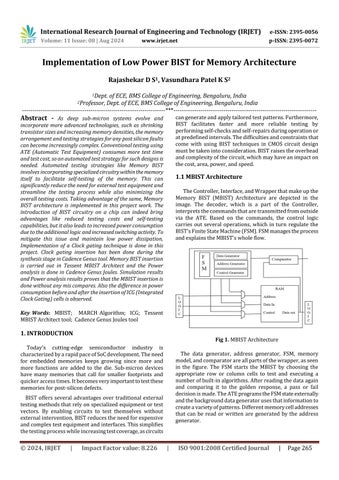
1.1 MBIST Architecture The Controller, Interface, and Wrapper that make up the Memory BIST (MBIST) Architecture are depicted in the image. The decoder, which is a part of the Controller, interprets the commands that are transmitted from outside via the ATE. Based on the commands, the control logic carries out several operations, which in turn regulate the BIST's Finite State Machine (FSM). FSM manages the process and explains the MBIST's whole flow.
Key Words: MBIST; MARCH Algorithm; ICG; Tessent MBIST Architect tool; Cadence Genus Joules tool
1. INTRODUCTION
Fig 1. MBIST Architecture
Today's cutting-edge semiconductor industry is characterized by a rapid pace of SoC development. The need for embedded memories keeps growing since more and more functions are added to the die. Sub-micron devices have many memories that call for smaller footprints and quicker access times. It becomes very important to test these memories for post-silicon defects.
The data generator, address generator, FSM, memory model, and comparator are all parts of the wrapper, as seen in the figure. The FSM starts the MBIST by choosing the appropriate row or column cells to test and executing a number of built-in algorithms. After reading the data again and comparing it to the golden response, a pass or fail decision is made. The ATE programs the FSM state externally and the background data generator uses that information to create a variety of patterns. Different memory cell addresses that can be read or written are generated by the address generator.
BIST offers several advantages over traditional external testing methods that rely on specialized equipment or test vectors. By enabling circuits to test themselves without external intervention, BIST reduces the need for expensive and complex test equipment and interfaces. This simplifies the testing process while increasing test coverage, as circuits
© 2024, IRJET
|
Impact Factor value: 8.226
|
ISO 9001:2008 Certified Journal
|
Page 265