
Design and Implementation of a Dual Stage Operational Amplifier
 Saumya Mishra1
1M.Tech Scholar, Department of ECE, Indira Gandhi Delhi Technical University for Women, Delhi, India ***

Abstract - Inthispaper,wehaveusedMillerCompensation Technique to amplify the gain of a 2-stage Op-Amp. Below mentioned procedure follows the technique of developing a theoretical design followed by carrying out a simulation processbypresumingsomevaluesforaparticularoperational situation (we’ve taken help of LTspice for that). The resultant CMOS Op-Amp was tested in a simulated parameter of VDD=1.8V in order to test the accuracy of theoretically concluded numbers. The CMOS technology used was 180nm with the help of LTspice tool. In the above mentioned environment; the following key factors were taken into observation: gain margin, phase margin, Output Power dissipation,outputNoise andunitygainbandwidth.
Key Words: Gain Margin, Phase Margin, Gain Bandwidth, Miller Compensation
1.INTRODUCTION
The road for the expanding market of sophisticated electronicsapplicationsinmobilesandsensorapplications wascreatedbytherecentdevelopmentinCMOSscaling.The integration of complicated functionalities on a single chip (such as a SOC (System on Chip)), along with ongoing increasesinoperatingspeedanddecreasesinsystempower consumption,iswhatdrivesscaling.[1]
Transistordimensionsaregettingsmallerasaresultof improvementsinCMOSmanufacturingtechniques[1].The advantages of adopting smaller dimension transistors typicallyresultinlowerpowerconsumption,smallerdevice sizes, and higher performance at high frequencies. Transconductanceandoutputresistance,twocrucialanalog propertiesofatransistor,willdecreaseasaresultoftheuse oftinyCMOStechnologies.
Analogcircuitsfrequentlyemployoperationalamplifiers (op-amps)withnegativefeedbacktocreateamplifierswitha variety of desirable characteristics, including steady gain, goodlinearity,andlowoutputimpedance[2].However,the negative feedback's significant phase lag causes a stability (STB)problem.TheSTBoftheamplifierhasbeenimproved usingavarietyofapproaches[3]-[5].
Thegainofasingle-stageopampisderivedbymultiplying transconductancewiththeoutputimpedance.Thegainand other crucial parameters such as output swing, gain bandwidth,etc.offeredbyvarioustopologiesofasingle-stage opamp such as Single stage Common Source Amplifier, Cascode Amplifier, etc. are insufficient for several
applications.Forinstance,amodernop-ampmustbeableto deliver single ended output swings of up to 0.8 V while operating with input voltages as low as 0.9 V. When this happens, we turn to "two-stage" operational amplifiers, in whichthefirststageisresponsibleforprovidinghighgain and the second stage provides large swings. A two-stage arrangement isolates the gain and swing requirements as opposedtocascodeopamps[7].
Therehasbeenmultipleresearchthatproduceda>140dB gain usingthe multi-stageamplifier technology, whichhas beenaroundforawhile.Thestabilityoftheopampsmaybe compromised by the close spacing of the poles caused by cascadingmanystages.
when we observe the second order system’s time response withstepinput, we see thatlarger phase margin resultsinreducedoscillationsintheoutputsignal[12][13]. we prefer to have ringing as minimum as possible. A minimumof45degreesphasemarginisdesirableanda60 degreePMismostlypreferred[12].
Frequencycorrectionmustbecarriedouttoimprovisethe stabilityandprovidepropertransientstepresponsiveness. Miller and cascode compensations are well-known approaches.Millercompensationiswellknownforitsability to increase bandwidth via pole splitting phenomenon. We will be employing miller compensation in our dual-stage opampandobservetheresultswithhighgainandimproved phase margin. Though miller compensation is used to enhance the gain bandwidth product, complexity has also risen as a result of interims of extra amplifier stages and capacitors. The stability is compromised by the right half
zero(RHP)thatisintroducedbyMillercompensatingwitha nullingresistor.[6]
Thepaperhasbeenorganizedasfollows,section-2deals withthetheoreticaldescriptionandSmallsignaldynamicsof dual-stageopampwhenitisuncompensatedaswellaswith miller compensation. Section-3 describes the design procedureofdualstageopampandsection-4summarizesthe prototyperesults.
2.
Opampsareusuallyconfiguredinnegativefeedbackmodeas canbeseeninaboveFig.1HereA(s)isthegainofAmplifier, F (s) is the transfer function describing external feedback fromtheoutputofopamptotheinput.


TheloopgainL(S)isgivenby,
In order to have a stable feedback system, we need to have,
Fig.3showsthesmallsignalmodelofanuncompensated Opamp.Thelocationoftwopolesofthismodelisgivenby,


and,
whereC1andC2arethecapacitancestogroundobserved fromthefirstandsecondstages,respectively,andR1 andR2 aretheresistancestogroundasseenfromtheoutputofthe firstandsecondstages,respectively.

It was found that the phase margin observed is significantly less than 45 degrees when an open loop frequencyresponseofnegativefeedbackiscomputedusing thementionedopamp,evenwhenconsideringtheworstcase scenarioofstability(consideringF(S)=1).Thissuggeststhe needforcompensationinthedualstageoperationalamplifier priortoit’sutilizationinaclosedloopconfiguration[12].
Where, is,
A close loop system's time response can be used to understandthesignificanceofgoodstabilitythatisacquired withsufficientphasemargin.Becauseithasbeenfoundthat alargerphasemarginreducesoutputsignalringing.Phase margins of at least 45 degrees are preferred, however in mostcases,60degreesisrecommended.
In this situation, the Miller effect results in making one poledominant whileweakeningtheother.Meaning,while one pole increases in frequency, the other decreases in
frequency. The Miller effect is frequently called as Miller compensation when this opposite motion (also known as polesplitting)isarequiredoutcome[13].


process parameters for CMOS 0.18um technology used in calculationofCMOSdesignparametersfordesigningadual stageopamp.
Table -1: Designspecificationrequiredtobemetbyopamp




In Fig. 5. the shift in the pole positions is depicted as they transition from their uncompensated locations to the compensated positions on the complex frequency plane. A verypopulartechniqueofusinganullingresistorhavebeen developed to overcome the drawback of the RHP zero introducedbytheMillereffect[12].

FromherewegettheValueof Let’sassume

by-
Byputtingthevalues,wearegetting
Fig. 5. explains the shifting of bode plot from an uncompensatedsystemtocompensatedsystem[12].
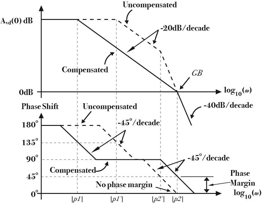
3. SCHEMATIC & DESIGN EQUATIONS OF DUAL STAGE OPERATIONAL AMPLIFIER
Table 1. shows the required opamp specification consideringwhichthedesigningisdone.Table2.depictsthe


By putting corresponding values and solving above equations,weget
Step5)DesigningofM5
Bysolvingaboveequationweget,
Step6)DesigningofM6&M7
For designing M6, first wewill find trasconductance of M6,


2.
By putting corresponding values and solving above equation,weget, 136


ForM7,
3. CONCLUSIONS
The Paper reviews and highlights drawbacks of uncompensated two stage opamp design. It signifies the improvement brought out in two stage opamp design by using miller compensation and implements miller compensation in designing two stage opamp highlighting improvedparameters.Theaspectratiovaluesobtainedfrom calculation shows better DC gain, Phase Margin and Gain Bandwidth Product of the implemented dual stage operationalamplifier
REFERENCES
[1] H.Iwai,"CMOSScalingTowardsItsLimits", Solid-State and Integrated Circuit Technology 5th International Conference,pp.31-34,October1998.
[2] H. Ju and M. Lee, "A Hybrid Miller-Cascode CompensationforFastSettlinginTwo-StageOperational Amplifiers," in IEEE Transactions on Very Large Scale Integration(VLSI)Systems,vol.28,no.8,pp.1770-1781, Aug.2020,doi:10.1109/TVLSI.2020.2986508.
[3] S.Liu,Z.Zhu,J.Wang,L.LiuandY.Yang,"A1.2-V2.41GHz three-stage CMOS OTA with efficient frequency compensationtechnique", IEEETrans.CircuitsSyst.IReg. Papers,vol.66,no.1,pp.20-30,Jan.2019.
[4] R.G.H.Eschauzier,L.P.T.KerklaanandJ.H.Huijsing,"A 100-MHz100-dBoperationalamplifierwithmultipath nested miller compensation structure", IEEE J. SolidStateCircuits,vol.27,no.12,pp.1709-1717,Dec.1992.

[5] "Multi-stage amplifier with capacitive nesting for frequencycompensation",Apr.1984.
[6] R. Nagulapalli, K. Hayatleh, S. Barker, S. Zourob, N. YassineandB.N.K.Reddy,"ATechniquetoReducethe Capacitor Size in Two Stage Miller Compensated Opamp," 2018 9th International Conference on Computing, Communication and Networking Technologies(ICCCNT),Bengaluru,India,2018,pp.1-4, doi:10.1109/ICCCNT.2018.8493494.
[7] Behzad Razavi, Design of Analog CMOS Integrated Circuits(1st.ed.),McGraw-Hill,2000.
[8] Z.Yan,P.MakandR.P.Martins,"TwoStageOperational Amplifiers: Power and Area Efficient Frequency Compensation forDriving a Wide Range of Capacitive Load", IEEE Circuits and Systems Magazine,vol.11,pp. 26-42,2011.
[9] Yao Libin, M. Steyaert and W. Sansen, "Fast-settling CMOS two-stage operational transconductance amplifiers and their systematic design", Proc. IEEE InternationalSymposiumonCircuitsandSystems,2002.
[10] P.R. Gray and R.G. Meyer, "MOS operational amplifier design-atutorialoverview", IEEE Journal of Solid-State Circuits,vol.17,no.6,pp.969-982,Dec.1982.
[11] S. I. Singh, "Design of low-voltage CMOS two-stage operational transconductance amplifier," 2017 International Conference on Electrical, Electronics, Communication,Computer,andOptimizationTechniques (ICEECCOT), Mysuru, India, 2017, pp. 248-252, doi: 10.1109/ICEECCOT.2017.8284677.
[12] Allen.P.E., and Holberg.D.R., “CMOS Analog circuit design” ThirdEdition,2019,OxfordUniversityPress
[13] TheMillerEffectandPoleSplitting©2000ThomasH.Lee, rev. October 17, 2003; https://web.stanford.edu/class/archive/ee/ee214/ee214. 1042/Handouts/HO9POLESPLIt.pdf