Modeling and Simulation Graphene based Nano FET : A Review
1Neha, 2Manoj Kumar
1Research Scholar, ECE Department, Om Sterling Global University, Hisar, Haryana (India)

2Associate professor, ECE Department, Om Sterling Global University, Hisar, Haryana (India)
Abstract: Graphene-based Field Effect Transistor modelling is described in this article. Utilizing SILVACO TCAD tools, modelling is completed. The structure is built usingthevirtualATLASframework,andthemodelisused to assess the efficacy of graphene-based FETs. To create the device structure, we first deposit a 5nm thick polysilicon layer rather than a graphene sheet. As the channelmaterial,grapheneisused,anditismodelledasa semiconductor with a 10,000 cm 2 /V-s carrier mobility. Theoutputcharacteristicandtransfercurveareplottedas characteristic curves with TONYPLOT. There is no band gap in pure graphene. As a result, it is regarded as a zero bandgap or semi-metal semiconductor. Because GFETs lack a bandgap and have a lower I ON/I OFF ratio than silicon-basedtransistors,theyarestilllessefficientforuse in digital logic circuits than Si transistors. Due to its extreme mobility, it is better suited for RF applications. Thus, in this article, it is possible to get the maximum cutoff frequency (f T) and the maximum oscillation frequency (f max), which are thought to represent the FOMsofRFtransistors.
Keywords: Graphene, grapheme based FET, GFET, Modelling
1. INTRODUCTION
Planar, two-dimensional, and just one layer thick, graphene is a crystallized form of carbon. It is a key component of fullerenes, carbon nanotubes, charcoal, and one of carbon-graphite's most significant allotropes. In order to generate extended benzene ring configurations, grapheneismadeupofsp2hybridizedcarbonatoms.With ameasuredelectronmobilityofupto250,000cm2V1s1 (suspended form), graphene is known to possess exceptional electrical characteristics as a result of its structure. Additionally, graphene has been shown to have remarkable mechanical qualities and to have the greatest breaking strengths ever measured (42 N-m-1). Additionally, graphene has great optical qualities, which allow it to be used in optical devices like light detectors. [1].
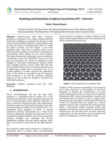
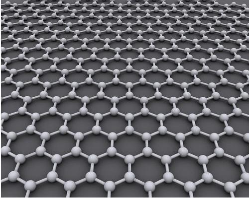
The structure's single atom of thickness is formed by a honeycomb lattice of carbon atoms, two-dimensional
structure known as graphene. In-depth analyses of each aspect of this unique substance have been sparked by its recentexperimentaldiscovery[2].
Graphene,whichhasbeenresearchedforaverylongtime and is often referred to as "2D graphite," is used most frequently to illustrate the characteristics of various carbon-basedmaterials.Therearemanywaysinwhichthe fundamental GFET, a three-terminal device, resemblesthe conventional FET. It consists of a drain, a supply, and a highorbackgate.Thesupplyanddrainmetalelectrodesof a GFET are separated from one another by a narrow graphenechannel,whichistypicallytensofmicronsthick, unlike a silicon-based junction transistor [3]The gate regulates the behaviour of the channel by dictating how electrons react. For the GFET, there are three major gate configurations. As indicated below, typical transistors will eitherhaveahighgate,aworldbackgate,orboth.
A GFET's gate regulates the flow of electrons or holes across its channel, much like the gate in vintage semiconductor FETs. The extraordinary sensitivity of the grapheneFETsisduetothefactthatallofthisflowsonthe surfaceofthejunctiontransistorchannel,whichisjustone atom thick. In semiconductor devices, current typically moves via electrons or holes. The GFET, however, allows for equal conductivity between electrons andholes. When a hole carrier is conducting in the channel region under a negative bias, GFET devices behave in a usual ambipolar manner. On the other hand, a positive bias causes lepton carrierconductivity[4].
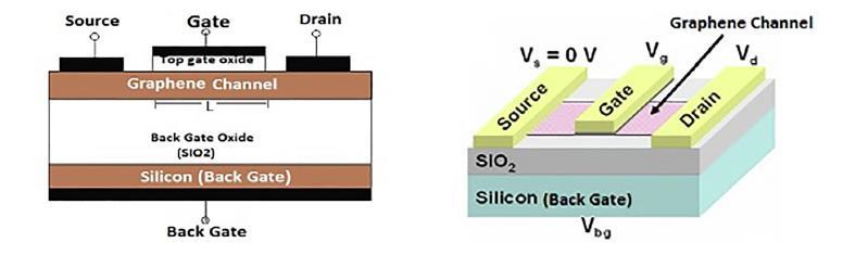
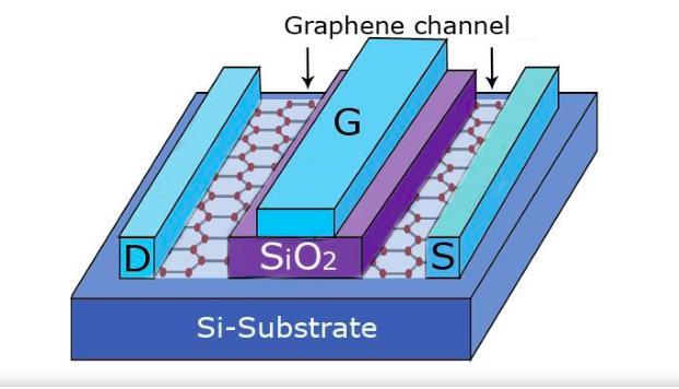
OnesuchdualgateG-FETimplementationisshowninFig. 3.Figure3(a)displays the2-dimensional read,and Figure 3(b) displays the matching three-dimensional read. The graphene channel is desired in this arrangement between two gate chemical compound layers, namely between the highgateandthereargatechemicalcompound(substrate) layers[5].TheSiO2servesasthereargate'sinsulator.The rear gate, or Si wafer,createsa veryinexpensivelayer. By depositing on a thick SiO2 layer, which was afterwards generated to develop on a heavily doped back gate that is that the Si wafer, the bilayer graphene channel is desired. Channelinversionmustoftenbeworndowninorderfora G-FET to function as a switch that switches between the ON and OFF states by applying the proper back gate bias voltage. The supply and drain resistance of the GFET are controlledbyreargate.
2. RELATED WORK
2.1 Someoftherecentrelatedworksaregivenbelow
The integrated graphene-based FET (GFET) biosensors at thenanoscalearethemaintopicsofthisstudy.Givenhow quickly it may spread from one person to another in only minutes,the newkindof coronavirus hasclearlyemerged as a severe problem in today's dynamic environment. Compared to other coronaviruses like SARS and MERS, COVID-19 may spread more quickly. Due to its resemblance in form under the electron microscope, the term corona is obtain from the Latin word definition "crown."Inorder to emphasizethis roadmap,some of the most current works are examined and examined for this goal.[6].
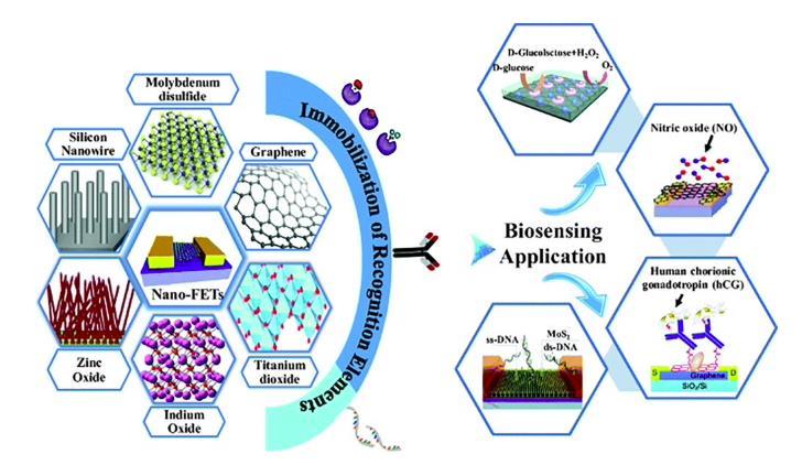
Its potential uses have generated a great deal of attention due to the exceptional electrical characteristics as well as good optical, mechanical, and thermodynamic qualities.
Theutilityof largearea grapheneasa channel material in MOSFETs has been constrained by its zero band gap. In addition to outlining a few techniques researchers have used to produce band gaps in graphene, this study also covers the fundamental physics of graphene. Along with a model for the current and charge densities in top gated Large Area Graphene FETs, a few graphene implementations in FETs and their findings are also provided.[7].
Now is the time to seriously consider finding alternatives to silicon for use in transistors. In the modern world, if Gordon Moore's forecast is to come true, the semiconductor industry will soon enter a post-silicon era. Nanomaterials generated from graphene are now being considered as potential post-silicon electronics device materials.Fieldeffectbehaviouringrapheneandgraphitebased devices is the main topic of this work, which also studies and analyzes it. Additionally, it gives a brief overview of graphene's theoretical characteristics before going through its properties as they relate to electrical devices and looking at how they affect the functionality of transistors made of graphene in both logic and radiofrequency applications. It is possible to draw the conclusion that graphene's outstanding mobility may not be its most enticing property from a device standpoint, contrary to what is often believed. Instead, GFFT may be able to overcome the unfavourable short-channel effects that restrict their performance by being scaled to shorter channel lengths and greater speeds if devices with very thinchannelsaredeveloped. [8]
In the last ten years, the study of graphene and its use in cutting-edge electronics has grown quickly. Post-silicon technology is increasingly necessary for industry as Moore's law starts to plateau. Additionally, terahertz detectors and receivers cannot be implemented using current technology, which are necessary for a variety of applications, including as security scanning and medical imaging. Due to its exceptional electronic properties, including observed electronic mobilities of up to 2 105 cm2 V1 s1 in suspended graphene samples, graphene is regardedasa keypotential candidate for replacingsilicon incurrentCMOStechnologyaswellasrealizingfieldeffect transistors for terahertz detection. In relation to the implementation of graphene transistors, this article examines the physics and electrical characteristics of graphene[9]. Mechanical exfoliation, chemical vapour deposition, and epitaxial growth are a few common methods used to create graphene Since graphene has a zero bandgap and is semi-metallic, this poses a problem for digital electronics applications and is one of the difficulties in fabricating graphene transistors. Consequently, the research also discusses several
techniques for opening a bandgap in graphene employing bilayer graphene and graphene nanoribbons. Key merit metrics used in the literature are extracted, and the fundamental workings of a typical field effect transistor are described. The overview of certain cutting-edge graphene field effect transistor examples is offered at the end, with a special emphasis on monolayer, bilayer, and graphenenanoribbons.[10]
This study provides a thorough overview of current advancements in graphene field effect transistors, taking into account a variety of factors including manufacturing, modelling and simulation tools, and applications, particularly in sensors, outlining the directions for the future. Due to silicon's limits in terms of shrinking transistor size, various alternative materials for manufacturing have been tested in order to comply with Moore's law and enhance the transistor density of an integrated circuit due to qualities like increased carrier mobility and very high trans-conductance gain, among others, one such material, graphene, demonstrates its suitability as a silicon substitute. Additionally, high-speed analogue VLSI, RF, and biosensor circuits are finding that G-FETisthebestalternative.[11].
3. NEED OF GRAPHENE-BASED FET
GFET Challenges
For silicon-based transistors, graphene FETs are a beautiful substitute. However, there are a number of difficulties that make industrial production difficult, includingthefollowing:
1) Bandgaplimitations
2) Fabricationprices
3) Saturation
Benefits of Graphene-Based FETs
Low resistance losses and greater cooling than semiconductors are the results of graphene's improved electrical and thermal conductivity. As a result, graphene transistors might provide improved performance and potency[12].
The entire channel is on the surface because the structure is only one atom thick. Thus, in detector applications, the channel is wide open to the material or surroundings underneath the look at. This makes some GFETs sensitive and appropriate for a variety of bio- and chemical-sensing applications[13]. For instance, it might pick up on a molecule sticking to or detaching from a surface. Not to mention, research has indicated that
employing a thin, top-gate dielectric material improves GFET properties like open-circuit gain, forward transmissionconstant,andcutofffrequency.Thisopensup the possibility of using GFETs in a variety of applications andforveryhigh-frequencyoperations[14].Theoretically, the junction transistor can change far more quickly than silicon-basedFETs,approachingtherateofchangeatvery high rates. Standard semiconductor materials' lattice structure has various restrictions that make it heatdissipaterapidlyathigherfrequencies.Ontheotherhand, the high lepton quality, polygonal form lattice structure, and other features change it to operate at the rate frequenciesmuchbetter.
4. MODELING & SIMULATION
Programme for G-FET modelling and simulation. This section compares a few of the widely available modelling and analytical tools for G-FET. GFET tool, which simulates conducting behavioural research on the electrical and thermal properties of a GFET. The G-FET's voltage and current can be calculated using this device while the GFET's temperature is kept constant[16] The tools for this inquiryemployadriftingtechniqueandaprolixitysystem. The following research projects on GFETs may also be estimatedandstartedusingthismethod,i.e.
a) Carrierviscosity
b) Temperatureprofilestudies
c) Drifthasteand
d) Electricfieldstudies
When creating the models for ATLAS simulator (a device simulator for 2D and 3D structures), Silvaco, a CAD programme, is utilised. This simulator aids in simulating the study of the electronic circuits' electric, optical, and thermal properties. It is simple to understand how the gadget operates thanks to these simulation studies. Theses,whicharecreatedusingemulsionaccessoriessuch as double, ternary, and quaternary, assist in creating an accuratecalculationofthebias[17].
MeterTheenormoussignalGFETforambi-polargraphene high frequency electronic circuits is modelled using the virtuoso spectre circuit simulator tool. In processes like the multiplier phase sensor, radio frequency sub harmoniousmixer,andfrequencydoppelgänger,thislarge signalmodelisfrequentlyused.ForRFoperations,thereis aparticularVirtusospectreinterpretation.Thetool,called Virtuoso Spectre RF, can be used to assess the DC and AC characteristics,theRCbirthfordetentionestimate,andthe electromagnetic (EM) analysis of GFET grounded circuits[18]
Sentaurus is a well-known EDA tool for simulating the GrapheneFETgroundeddetectorsusedinthedetectionof single beachfront DNA (also known as ssDNA) and reciprocal DNA(alsoknown ascDNA)(10).Itisa cuttingedge design and optimisation tool for GFET grounded circuits. This may aid in creating device simulations in severaldimensions.Thesimulationmayincludeastudyof the physical properties of electric, optical, or thermal systems. Electronic biases of the semiconductor grounded orcombinationalkindarealsopossible[19].
5. APPLICATIONS OF GRAPHENE
Due to its remarkable properties, graphene may be employed in a broad variety of applications Hereareafewpotentialusesforgraphene:
RF circuits (because to the high mobility values reportedinit)andsignificantcutofffrequenciesin graphene field-effect transistors (for instance, Lin et al.'s study showed that graphene nanoribbonbased FETs had cutoff frequencies of 100 GHz). Any of the aforementioned techniques may be usedtocustomizeabandgapinlogiccircuits.
Since graphene is more transparent and flexible thanthelesstransparentandmorebrittleindium tin oxide that is currently employed in the industry, it may be used to build transparent electrodesforsolartechnology.
Due to its semi-metallic behaviour with high mobility and strong flexibility[20], interconnect applications.
Graphene may one day be utilized to make supercapacitorsbecauseofitshighsurfaceareato volumeratio.
6. CONCLUSION
The operate of graphene in logic circuits is presently not practical due to low on/off current levels. Due to its high mobility and highcutoff frequency,it may be employed in RC circuits, but the issue of large off currents still exists and resulting in much greater power dissipation than the existing, highly low powered CMOS technology Further study may enable the creation of bandgaps in graphene without significantly reducing mobility, resulting in the creation of graphene FETs with a favourable on/off current ratio and great mobility. So, in the next years, graphene may replace other materials as the primary componentofelectricalgadgets.
REFERENCES
[1] K.S. Novoselov, A.K. Geim, et al.: Electric field effectinatomicallythincarbonfilms.Science.306, 666(2004)
[2] P.R. Wallace, The band theory of graphite, Phys. Rev.71(1947)622–634.
[3] M.C. Lemme, Current status of graphene transistors, Solid State Phenomena 156–158 (2010)499
509.
[4] Hague, J.P.: Tunable graphene band gaps from superstrate-mediated interactions. Phys. Rev. B. 84,155438(2011)
[5] Sahu, S., Rout, G.C.: Model study of the effect of coulomb interaction on band gap of graphene-onsubstrates.Phys.B.461,49(2015)
[6] J. Coraux et al., Structural coherency of graphene onIr(111),NanoLett.8(2008)565–570.
[7] T. Thingujam, K. Jolson, M. Kumar, S.K. Sarkar, TCADbasedmodellingandsimulationofgraphene nanostructured FET (GFET) for high frequency performance,Thingujam,AJET6(2017).
[8] F. Pasadas, D. Jiménez, Large-signal model of graphene field-effect transistors part II: circuit performance benchmarking, IEEE Trans. Electron Dev.63(2016)1–6.
[9] Virtuso RF tool: https://www.cadence.com/en_US/home/tools/cu stom-icanalog- rf-design/custom-ic-analog-rfflows/virtuoso-rf-solution.html
[10] J. Yunfang, J.u. Cheng, Sentaurus based modelling andsimulationforGFET’scharacteristicforssDNA immobilization and hybridization, J. Semiconduct. 37(2016).
[11] S.Rodriguezetal.,AcomprehensivegrapheneFET modelforcircuitdesign,IEEETrans.ElectronDev. 61(2014)1199–1206.
[12] S. Bardhan, M. Sahoo, H. Rahaman, A surface potential based model for dual gate bilayer graphene field effect transistor including the capacitiveeffects,J.CircuitsSyst.Comput.(2019).
[13] Lemme, Max C., et al. "A graphene field-effect device."ElectronDeviceLetters,IEEE28.4(2007): 282-284.
[14] Kim,Seyoung,etal."Realizationofahighmobility dual-gatedgraphenefield-effecttransistorwithAl 2 O 3 dielectric." Applied Physics Letters 94.6 (2009):062107-062107.
[15] Liao, Lei, et al. "High-κ oxide nanoribbons as gate dielectrics for high mobility top-gated graphene transistors." Proceedings of the national academy ofsciences107.15(2010):6711-6715.
[16] Xia, Fengnian, et al. "Graphene field-effect transistors with high on/off current ratio and large transport band gap at room temperature." Nanoletters10.2(2010):715-718.
[17] Thiele, S. A., J. A. Schaefer, and F. Schwierz. "Modeling of graphene metal-oxidesemiconductor field-effect transistors with gapless large-area graphene channels." Journal of AppliedPhysics107.9(2010):094505.
[18] Lin, Y-M., et al. "100-GHz transistors from waferscale epitaxial graphene."Science 327.5966 (2010):662-662.
[19] Meric, Inanc, et al. "Current saturation in zerobandgap, top-gated graphene field-effect transistors." Nature nanotechnology 3.11 (2008): 654-659.
[20] Schwierz, Frank. "Graphene transistors." Nature nanotechnology5.7(2010):487-496.