
Experimental Electrical Characterization Results of PLL Jitter
Nidhi1, M. Ejaz Aslam Lodhi2, Mohd. Safdar Imam31M. Tech. Scholar, Department of ECE, Indira Gandhi Delhi Technical University for Women, Delhi, India
2Senior Assistant Professor, Department of ECE, Indira Gandhi Delhi Technical University for Women, Delhi, India
3Sr. Manager, ST Microelectronics Pvt Ltd, Greater Noida, India

Abstract - In this letter, we aim to validate and check the electrical characteristic of Analog IPs embedded in SoCs. Analog blocks are more prone to the external behavior because the human world can talk and think in an analog manner. Hence, not easy to satisfy the requirement from an analogpointofviewcomparedtodigitalcircuitswhichcanbe simulated and tested. Furthermore, when an analog comes into the picture, the noise insertion and its interface connections start creating problems in satisfying the actual specifications.ElectricalcharacteristicsvalidatedonSoCsare single period and long-term Jitter for PLLs and their functionalityaccordingtothespecifications.Further,ourwork willbebasedonimprovingthetestbenchwithautomatedtest environment,sinceautomationhelpstoreducehumanerrors and make the testing process more reliable
Key Words: PLL, Jitter, Noise, Analog, SoC, Validation

1. INTRODUCTION
A phase-locked loop (PLL) is an electronic circuit that continuously modifies its voltage or voltage-driven oscillator'sfrequencytomatchthatofaninputsignal.PLLs can produce, maintain, modulate, demodulate, filter, or recoverasignalfromacommunicationschannel[1]thatis "noisy" because data is being interrupted. PLLs (PhaseLockedLoops)areessentialcomponentsinmanywireless andradiofrequency(RF)applicationsduetotheirabilityto generatestableandprecisefrequencies.Theyplayacrucial role in various communication systems and devices, including Wi-Fi routers, broadcast radios, walkie-talkie radios, televisions, and mobile phones. Here's a brief explanation of how PLLs are used in these applications, which further helps in low power and delay electronics device[8].APLLisusedforclockgenerationinsideSoC,and itsworkingandapplicationareprettysimilartoafrequency synthesizerinacellphonetomatchthecellphonefrequency withdesiredfrequencyofreceptionofthemessagesignal, thencommunicationcantakeplace.Thecorefunctionofa PLListosynchronizethephaseandfrequencyofanoutput signal with that of a reference signal. This closed-loop feedbacksystemallowsthePLLtolockontoandtrackthe phase and frequency of the reference signal, making it an essentialtoolinmanyapplications.Itisasystemofanalog anddigitalcomponentsconnectedina"negativefeedback" topologyratherthanasinglecomponent.
2. PLL AND ITS BASIC BUILDING BLOCK
APLLconsistsofthreekeycomponents:
1. Phase detector (aphasecomparatorormixer).It comparesthephasesoftwosignalsandgeneratesa voltage according to the phase difference. It multiplies the reference input and the voltagecontrolledoscillatoroutput.
2. Voltage-controlled oscillator produces a sinusoidalsignalwhosefrequencymatchesclosely thelow-passfilter'scentrefrequency.
3. Low-pass filter:theloopfilterplaysacrucialrole insmoothingandshapingthecontrolvoltagethatis appliedtotheVoltage-ControlledOscillator(VCO). Its primary function is to attenuate the highfrequencyalternatingcurrent(AC)componentsof the phase detector's output signal while allowing the low-frequency components (DC) to pass through relatively unattenuated. This action smoothensandflattensthesignal,makingitmore DC-likeorcontinuous
Tobetterunderstandtheoperation,let`sstartwiththebasic buildingblocksofPLL
The phase detector (PD) compares the phase difference betweentheinputsignal'sfrequency(f_ref)andthefeedback signal'sfrequency(f_out).ItdoesnotgenerateaDCvoltage directlyproportional tothe phasedifference, butrather it producesavoltagethatrepresentstheinstantaneousphase errorbetweenthesetwosignals.
The phase detector can be represented by a phase comparatororamultiplier.Whenusingamultiplierasthe
phasedetector,theoutputsignalwillcontaintwofrequency components:
Thesumfrequency:Thiscomponentisequaltof_in+f_out.It arisesbecausethephasedetectormultipliestheinputand feedbacksignals,producingthesumoftheirfrequenciesas oneoftheoutputcomponents.
Thedifferencefrequency:Thiscomponentisequalto|f_inf_out|, where the absolute value is taken to ensure it is a positive frequency. This component also appears in the output because of the multiplication process in the phase detector..
WhennoinputissuppliedtoaVCO,itgeneratesasignalata specific frequency. A DC voltage can be applied to this frequency to move it in either direction. The frequency deviation is thus directly related to this. The voltagecontrolled oscillator signal is compared to the input/reference signal by the PLL. The PLL can identify frequencyandphasediscrepanciesinthesignalsbecauseit isfrequencyandphasesensitive.Itproducesorgeneratesan error signal that reflects the phase difference in the transmission.Thelow-passfilter(LPF)usesthisdifference, which is an error signal to remove high-frequency componentsandconverttheerrorsignaltochangingdirect current (DC) levels. The voltage-controlled oscillator is subsequently given this "feedback signal" in order to regulateitsfrequency.
3. JITTER AND ITS TYPES

ManyofthesignalsinsideaPLL,aswellasthoseattheinput andoutput,arebinarysignals.Thejitterofbinarysignalsisa frequent way to describe noise. An unwanted change or ambiguity in the timing of occurrences is known as jitter. Typically, the transitions in a signal are the events of interest.
Figure 2 [2]depicts a single period, or cycle, of a signal containing numerous distinct periods. An ideal waveform exhibits a consistent and repetitive cycle. However, realworldwaveformsvaryinthetimedomain,withsignaledges either rising or falling earlier (red) or later (blue) than expected. Jitter is introduced due to slight instabilities in electricalsignalreadingequipmentandinterferencealong signal-carrying paths. Excessive jitter can lead to interference between neighboring signals, resulting in a degradationofimageandsoundqualityduringtransmission.
1. TypesofJitter:Therearemanytypesofjitter,including thefollowing:
- Periodjitter(peaktopeak)
- RMSjitter
- Randomjitter
- Deterministicjitter
- Accumulatedjitter(long-termjitter)
Wewillbecalculatingperiodandlong-termjitter. Periodjitter(peak-to-peakjitter)
1.1. Period jitter isobservedasvariationwidth.Epson expresses this variation using a peak-to-peak value.
1.2. RMS jitter (1-sigma)Thestandarddeviation(a)of the above measurement findings is used to calculate RMS jitter. This indicates a 68.26% chance that it exists within 12.5 p. Peak-to-peak jitter, on the other hand, only reveals a small percentageofstates(manyms)inacrystalproduct thatistypicallyusedforanextendedperiodoftime anddoesnotexhibitoveralljitter.RMSjitterisonly a meaningful measurement for an ideal normal distribution (Gaussian distribution); it is exceedinglyunreliableforotherdistributions.
1.3. Random jitter (RJ)Asthenamesuggests,random jitter is a jitter component that cannot be predicted.Randomjittercanoccurspontaneously as it is influenced by a device's characteristics, thermalnoise,etc.Randomjitterisexpressedusing standarddeviation,usingtheexpressions"rightRJ" and"leftRJ."
Figure 2: Jitter
Digital signal waveforms show up as a bright line on an oscilloscope.Itispossibleforthisbrilliantline,whichshould oscillate frequently, to appear thick at times. A jitter is indicatedbythesignallineexpanding..
1.4. Deterministic jitter (DJ), Circuit design, electromagnetic induction, or the external environmentcanallinduceboundedjitter.Actual measurement findings show that deterministic jitter is the part between right and left random jitter. To summarise the preceding jitter ideas, spontaneously induced jitter (RJ) and artificially inducedjitter(DJ)arecomponentsof theoverall jitter in a single cycle length. Reducing deterministicjitteristhekeytodecreasingjitter. When this component is optimized, the gap betweentherightandleftRJoverlaps,allowinga perfectnormaldistributiontooccur.
1.5.
Accumulated jitter (long-term jitter)
Accumulatedjitterisatypeofjitterthatcannotbe described as variations within a single cycle or period. Instead, it results from the cumulative effect of jitter fluctuations observed over numerous successive cycles. In this context, the horizontal axis of a jitter plot represents the numberofmeasuredcycles,whiletheverticalaxis depictsthejitter's1-sigmavalueforeachcycle. Analyzingaccumulatedjitterallowsustoobserve thebehaviorofjitteroverconsecutivecycles.With accumulatedcycles,thereisatendencyforthe1sigmajittervaluestoconvergeorstabilizestarting from a certain cycle. This means that as more cyclesareconsidered,thejitterfluctuationstendto reach a relatively consistent level, providing insightsintothelong-termstabilityandbehaviorof thejitterphenomenon.ThisenablesthePLLcircuit bandwidthandtransientresponsecharacteristics tobedetermined[2]
Jitterhasanimpactonthesetupandholdoftheroute elementsbecauseitaltersthecircuit'sclockdelayand theamountoftimetheclockisavailableatsyncpoints. Depending on whether the jitter makes the clock run faster or slower in a system that otherwise has clean timing,setupholdorsetupviolationsmayhappen.Asa result, the chip's functionality or performance will degradeand,whenanalysingtiming,thedesignermust takeintoaccountthejittervaluesoftheclocksignal.
PLL testing is an essential part of validation. Our primary focus is to use PLL inside the SoC to provide a variable frequency clock input to many blocks and the peripherals attachedto SoCfortheir data transfersynchronization. In sucharchitecture,PLL0andPLL1areconnectedincascaded mode,andthesourceclocktoPLLcanbeprovidedbyanyof thethreeavailablesources,i.e.,IRC(16MHz),XOSC(40MHz), andexternallybyAWG.
The test execution is done in automation to avoid human errors.Atthesametime,itisalsocumbersomeforahuman tocollectsomuchdatamanually.Allthebenchinstruments areconnectedtogethertothePCthroughtheGPIBinterface, an IEEE interface standard that allows control of the equipment remotely. The test automation is achieved throughVBA(visualbasic forapplication).AVBAscriptis writtentocontroltheseinstrumentstochangetheirvoltage supply and temperature, capture the data through an oscilloscopeandlogthemintotheExcelreportfileandusing pivotchart,weplotthegraphtohavetheunderstandingof results
4.1 Equipment Used to Perform Testing
1.4GHzOscilloscope
2.PrecisionTemperatureForcingSystem(PTFS)
3. Arbitrary Waveform Generator (80MHz) for applying externalclock.
4. Lauterbach Debugger Hardware with JTAG connection interface.
5.Activeprobe.Oneend is connectedto Oscilloscope,and anotherisconnectedtothePLLclockoutprobingpointon Daughterboard.
4.2 Validation Condition for IPs
Temperature: Table -1: Temperaturerequiredfortestingthe PLL
Table -2: MaximumandMinimumPowersupplyRequired fortestingthePLL
NumberofSamples:
The number of trials should be done on three samples to avoid discrepancies. It could be extended to more if the result is not compliant with the expected to ascertain if a particularobservedissueisreallypresentontheIPornot
4.3 Types of Test Codes for PLL
There are two types of test codes under which the PLL is tested,QuietModeCodeandApplicationlikeCode(Run_Idd Mode)
InQuietmodeCode,all IPs presentinsidetheSoC arenot active,onlythePLLundertestisactivatedandacoupleof otherIPsarereallyneededfortheSoC.MostoftheIPsare keptunderpowerdown.Atthistime,fewertransistorsare going through transitions, which means only a few are switchingon-off.Thisassuresthatthereisminimumnoise generatedinsidetheSoC,andPLLisminimallyaffectedby thenoiseinsidetheSoC.
Ontheotherhand,anApplicationlikecode(Run_IddMode) is used, and most of the IPs inside the SoC are enabled/activated. This way, the maximum number of possible transistors are going through transitions means gettingswitchedon–off. ThiscreatesnoiseinsidetheSoC andisnormallytheactualusecaseunderwhichPLLhasto work.
We perform the Jitter test on both types of codes. The parameters we measured in validations are Short-Term (SinglePeriod)JitterandLong-TermJitteronboththePLLs, which are embedded inside the 32-bit microcontroller architectureSoC
4.4 Software Development
Auniquesoftwarecodehastobedevelopedbyconfiguring the PLLs under test to generate the desired output clock frequencyasperthetestcases.
5. EXPERIMENTAL RESULTS
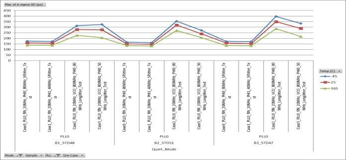
The above experimental results of consolidated Single PeriodJitterandlongtermJitterofPLL0QuietModewhich made us to conclude that the results are under the specificationprovidedbythedesignteamwhichare:
specified bythe designer
Wecanalsoconcludethattheresultsoflongtermjitterare high as compared to single period jitter because of the obviousincreasednumberofcyclesusedinlongtermjitter.
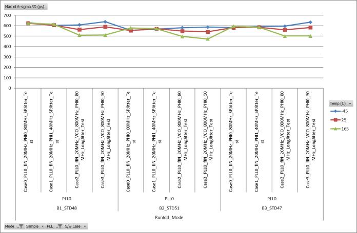
The above experimental results of consolidated Single Period Jitter and long term Jitter of PLL0 Run Idd Mode whichmadeustoconcludethattheresultsarenotunderthe specificationprovidedbythedesignteamwhichare:
Table-2:
Thereasonbehindtheresultsarenotunderthespecification areinRunIddmodeisemployed
The majority of the SoC's IPs are turned on or activated. In this manner, the most transistors possibleareswitchingonandofforpassingthrough transitions.
ThiscausesnoiseinsidetheSoCandistypicallythe usecasethatPLLhastooperatein.
Case Case5 Single period 105.522
ps
Max. Value after testing
338.934
Max.value specified bythe designer
Table-3: ResultsofSinglePeriodJitterPLL1(QuietMode)
Chart-4: SinglePeriodJitterPLL1:Run_Idd_Mode
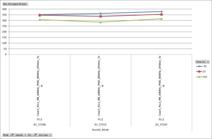
The above experimental results of Single Period Jitter of PLL1 Run Idd Mode which made us to conclude that the resultsare under thespecificationprovided bythe design team,whichis:
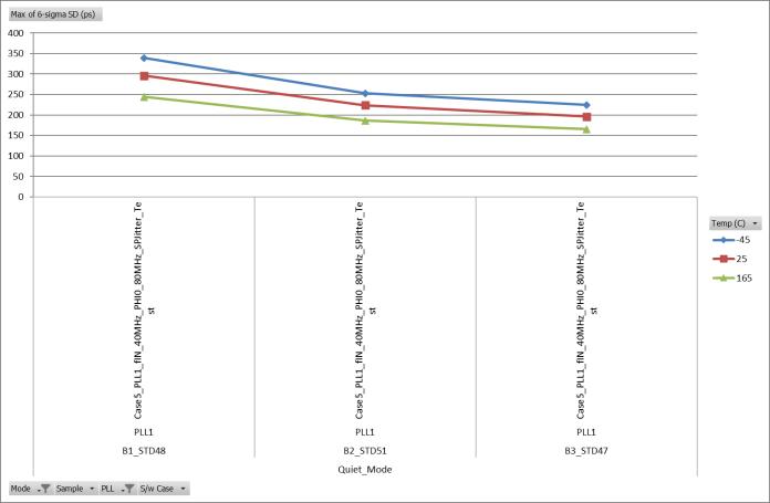
Case Typeof Jitter Min Value after testing Case
5 Single period 187.602 ps
ps 500ps
Table-4:ResultsofSinglePeriodJitterPLL1(Run_Idd_Mode)
Chart-3:
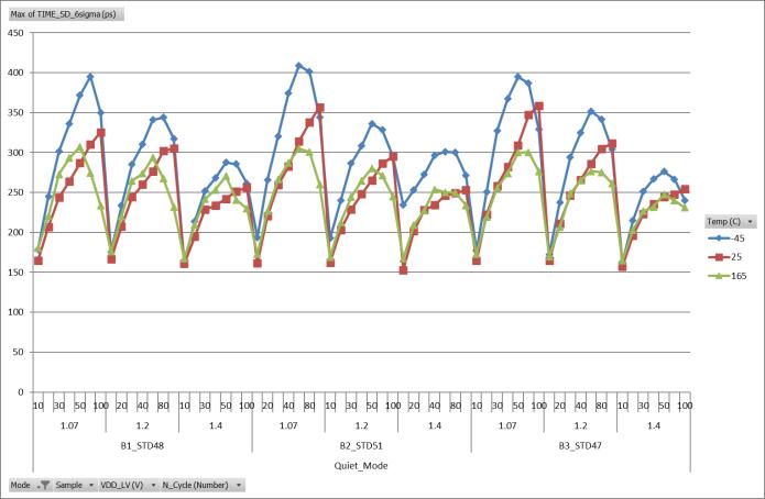
one thing we can observe in the graph that we are gettinglowerstandarddeviationatthetemperature165 Catthehottest.
Chart-5: LongTermJitterPLL0:QuietMode
The above experimental results of Single Period Jitter of PLL0QuietModewhichmadeustoconcludethattheresults are under the specification provided by the design team, whichis:
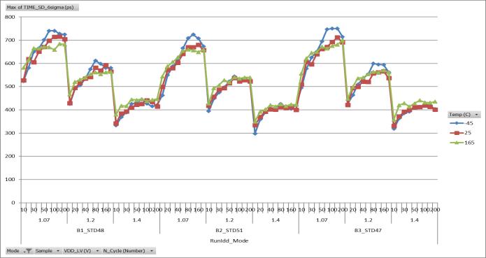
TheaboveexperimentalresultsofLongtermJitterofPLL0 RunIddModewhichmadeustoconcludethattheresultsare underthespecificationprovidedbythedesignteam,which is:
Table-5: ResultsofLongTermJitterPLL0(QuietMode)
All threesamples(SoC)used duringthe testingof are followingalmosthavingsimilarbehaviour,whichmakes ustojustifythattheresultswearegettingareaccurate andcanbeused
One thing we can observe in the graph that we are gettinglowerstandarddeviationatthetemperature-45 Catthemintemperature.
Chart-6: LongTermJitterPLL0(Run_IddMode)
Case Typeof Jitter Min Value after testing
Max Value after testing
Max value specifiedby the designer Case

ps 750.456 ps 1000ps
Table-6:ResultsofLongTermJitterPLL0(Run_IddMode)
All threesamples(SoC)used duringthe testingof are followingalmostsimilartrend,whichmakesustojustify thattheresultswearegettingareaccurate
6.
Once the measurements are done, data is plotted, and the result is analyzed. After analyzing the plotted results, it’s observed that all samples tested follow almost the same temperatureandvoltagevariationstrends.Bycheckingtheir minimum & maximum values, we can conclude that the resultsarewithinthedesignspecificationsornotunderthe testedVTconditions.
It'sobservedthatjitterwithapplicationlikecode(Run_Idd), ismuchhigherwithrespecttothequietmodecode,because a lot more transistors are switching, creating more noise insidetheSoCintheformercase.
PLLJitteralsoincreasesifunwantednoiseisgeneratedby anyparticularIPinsidetheSoC,affectingthePLL
Thermal noise, power supply changes, loading situations, device noise, and interference coupled with surrounding circuitsalsocontributetojitter.
Table -3: ResultsofthePLL Test Overview Condition Results
The test aimed to check the single period and longterm jitter.
REFERENCES
Temp:-40C,25C,165C
VDD-HV;3V,6V
VDD-LV:1.07V,1.2V, 1.40V
Fin:20/40MHz, Fref=Xosc
VCO:800MHz
PLL0PHI:40/80MHz
ClockoutonPad: 40MHz
MinVariation:0.00215%
MaxVariation: +0.0125%
[1] Awati,Rahul,andJohnBurke.“WhatIsaPhase-Locked Loop(PLL)?” Networking, 14 June 2021, www.techtarget.com/searchnetworking/definition/pha se-locked-loop.
[2] Jenkins, Julian. “Specifyinga PLL Part2: JitterBasics.” Design And Reuse, www.designreuse.com/articles/48875/specifying-a-pll-jitterbasics.html.Accessed15July2023.
[3] Maneatis,JohnG."Low-jitterprocess-independentDLL andPLLbasedonself-biasedtechniques." IEEE journal of solid-state circuits 31.11(1996):1723-1732.
[4] Georgoulopoulos, Nikolaos and Alkiviadis A. Hatzopoulos.“UVM-basedVerificationofaDigitalPLL Using SystemVerilog.” 2019 29th International SymposiumonPowerandTimingModeling,Optimization and Simulation (PATMOS) (2019):23-28.
[5] D. C. Lee, "Analysis of jitter in phase-locked loops," in IEEE Transactions on Circuits and Systems II: Analog and Digital Signal Processing, vol. 49, no. 11, pp. 704711,Nov.2002,doi:10.1109/TCSII.2002.807265.
[6] (JitterandPhaseNoise,n.d.)
[7] Telba, A.A. & Qasim, Syed Manzoor. (2011). ExperimentalInvestigationofLow-JitterandWide-Band DualCascadedPLLSystem.10.1063/1.3627194.
[8] HarshitaGehlot,MohdEjazAslamLodhi,“Analysisof ProposedFinFETBasedFullAdderusingCMOSLogic Style”, International Research Journal of Engineering andTechnology,Vol.6,(04),April2019