
Design And Analysis Of 64-Bit Adders In Cadence Using Different Logic Families
1Gadamsetty Vyshnavi, 2Pasupulati Vijay Krishna1Student, Dept. of Electronics and Communication Engineering, GITAM University, Telangana, India

2Student, Dept. of Electronics and Communication Engineering, GITAM University, Telangana, India
Abstract -In this project, we focus on the design and analysis of 64-Bit Adders using different logic families: CMOS, Pseudo-NMOS, and Transmission Gate. Full-Adder circuits are digital logic circuits capable of adding two input bits and a carry-in bit and generating a sum and carry-out bit as outputs. They are an essential building block for larger Adders and are widely used in digital circuits. To design the Adder circuits, we use the design tools provided by Cadence. We implement the Full-Adder circuits using the appropriate MOSFETs for each logic family and cascade several Full-Adders together to form the larger 64-Bit Adder. Once we design the adder circuits, we use simulation tools to verify their functionality and compare their power and performance characteristics. We measure the power consumption of the adder circuits under different operating conditions and analyze the speed of the adder circuits to determine which logic family offers the best trade-off regarding power efficiency and performance. Based on the results obtained from different logic families, we can identify the logic family that provides the best combination of speed and power consumption.
Key Words: Full Adder, Ripple Carry Adder, CMOS, Pseudo-NMOS,TransmissionGate,PowerAnalysis
1. INTRODUCTION
We are seeing rapid growth in the field of integrated circuit (IC) technology. All ICs must be designed in an optimized manner to meet all requirements of speed, space-saving, and low power consumption. One of the circuits that most ICs occupy is the ALU, which is a combination of arithmetic and logic units. The two most importantarithmeticunitsareaddersandmultipliers.
Adders are the heart of arithmetic circuits, and many complex arithmetic circuits are based on addition. Due to the widespread use of this operation in arithmetic functions, adders in mobile applications are of interest. Several variations of different logic styles have been proposed in recent years to implement 1-Bit adder cells. These summing cells are typically intended to reduce power consumption and increase speed. These studies alsoexploredifferentapproachestoimplementingadders usingCMOStechnology.
In mobile applications, designers must work within very tight leakage performance specifications to meet battery lifeandpackagecostgoalsfortheirproducts.Adesigner's concern about the level of leakage current has nothing to do with ensuring correct circuit operation but with minimisingpowerconsumption.
Inthisproject,allthedesignsarebasedonthestructureof theRippleCarryAdder.Sinceitis a 64-BitFull-Adder, we cascaded 1-Bit, 4-Bit, 8-Bit, 16-Bit, and 32-Bit together to form a 64-Bit using Ripple carry Adder for each logic family. These Full-Adders of all logic families and their respective symbols are designed in GPDK090 and analyzedusingtheCadenceVirtuosoplatform.
1.1 Full Adder
A Full-Adder is a digital circuit. A 1-Bit Full-Adder adds three 1-Bit inputs named X, Y, and Cin. X and Y are the operands, and Cin has some carryover from the previous lesscriticalstage.AFull-Adderistypicallyonecomponent of a cascaded adder that adds binary numbers of 4, 8, 16, 32, etc. bits. This circuit produces a 2-Bit output Carry (Cout)andSum(S).
Equations: These equations are obtained from the truth tableof1-BitFull-AdderusingK-mapsforSandCout.Fig1 shows the circuit diagram designed from these equations:

Sum(S)=(XXORY) XOR Cin
Carry(Cout)=X·Y+Y·Cin+X·Cin
1.2 Logic Families
A logic family of monolithic digital integrated circuits is a group of electronic logic gates built using several designs, often compatible with logic levels and performance characteristics.
Alogicfamilycanalsobeasetoftechniquestoimplement logic in VLSI integrated circuits, such as a central processing unit, memory, or other complex functions. Some of these logic families use static techniques to reducedesigncomplexity.Otherlogicfamiliesofthistype, such as domino logic, use clocked dynamic methods to minimisesize,powerconsumption,andlatency.
Thelogicfamiliesusedinthisprojectare:
1. Pseudo-NMOS
2. ComplementaryMetalOxideSemiconductor (CMOS)
3. TransmissionGate
1)Pseudo-NMOS: Thisstreamlinedstructurereplacesthe pull-up circuit with a single pull-up PMOS whose gate is permanently grounded. Pseudo-NMOS works similarly to NMOS logic. When an NMOS transistor receives a significant voltage, it is called a closed circuit. In contrast, when an NMOS transistor gets a voltage of about 0 volts, the source-to-drain connection breaks, called an open circuit.
2) Complementary Metal Oxide Semiconductor (CMOS): CMOS combines NMOS and PMOS. Hence required number of transistors for designing a circuit is 2n. The Complementary Metal Oxide Semiconductor (CMOS)logicfamilyisadigitallogiccircuitwidelyusedin modernelectronicdevices.PMOStransistorsaredesigned tohavelowresistance between sourceanddraincontacts when the low gate voltage is applied and high resistance when a high gate voltage is applied; It's the opposite. The CMOS circuit is built with an additional configuration, which features low power consumption, strong antiinterferenceability,andhigh-speedoperation.
3) Transmission Gate: TheTransmissionGatehasNMOS and PMOS parallel to each other. The work is based on NMOSandPMOS.Astheinputishigh,NMOSgetsON,and when intake is low, PMOS gets on. As a result, the signal willpassthroughthecircuitandbeobtainedattheoutput.
1.2 Power Analysis
Power analysis is a crucial step in VLSI (Very Large Scale Integration) circuit design used in modern electronic devices such as smartphones, computers, and
microcontrollers. Power analysis involves measuring and analysing the power consumption as it affects circuit performance, as high power consumption can slow things down.
TypesOfPowerAnalysis:
Total-Power: It is the sum of the power consumed by all of its components, known as Total-Power. It is measured inwatts(W).
Average Power: It is the ratio of total power consumed overagivenperiodtothedurationofthatperiod.Itsunits arewatts(W).
Power Delay Product (PDP): Product of current consumptionanddelay.Itcanreflectbothdynamicpower consumption and propagation delay of the system. It is typicallymeasuredinjoules(J).
Peak-Power: The highest power value is observed at a given time and is measured in Watts (W) or MilliWatts (mw).
2. IMPLEMENTATIONS
2.1 CMOS 1-Bit Schematic
The schematic shown in Fig -2 is designed using FullAdderequationswithCMOSlogic,andaCMOS1-Bitcircuit iscreatedasasymbolnamedCMOS_1BIT.Fig-3showsthe symbolof1-BitCMOS.
InFig-2,a,b,andcareinputsandcarry,sumare outputs.
In Fig -3, V-pulse is connected to the inputs a,b, andcin individuallyand given voltage1 as0vand voltage2as1.8v.
V-pulse for a, b and cin is provided with periods 20us,40us,and80uswithpulsewidth10us,20us, and40us,respectively.
Vddisconnectedtotheground.
Using ‘DC Transient Analysis’, we have simulated thecircuit.
The graph in Fig -4 shows the transient analysis of CMOS 1-Bitwithastoptimeof100us.

Similarly,twoCMOS8-Bitaddersarecascadedtodesigna CMOS 16-Bit adder then two CMOS 16-Bit adders are cascadedtodesignaCMOS32-Bitadder.ItisshowninFig6.


TodesignaCMOS4-Bitadder,fourCMOS1-Bitaddersare cascaded. Then, two CMOS 4-Bit adders are cascaded to designaCMOS8-Bitadder.ItisshowninFig-5.
Similarly,twoCMOS32-Bit addersare cascadedto design aCMOS64-Bitadder.ItisshowninFig-7.


2.2
The schematic shown in Fig -8 is designed using FullAdder equations with Pseudo-NMOS Logic, and PseudoNMOS 1-Bit Circuit is created asa symbol named PseudoNMOS_1BIT. Fig -9 shows the symbol of 1-Bit PseudoNMOS.
InFig-8,a,b,andcareinputsandcarry,sumare outputs.
In Fig -9, V-pulse is connected to the inputs a, b, andcin individuallyand given voltage1 as0vand voltage2as1.8v
V-pulse for a, b and cin is provided with period 20us, 40us, 80us with pulse width 10us, 20us, 40usrespectively.
Vddisconnectedtotheground.
Using ‘DC Transient Analysis’, we have simulated thecircuit.
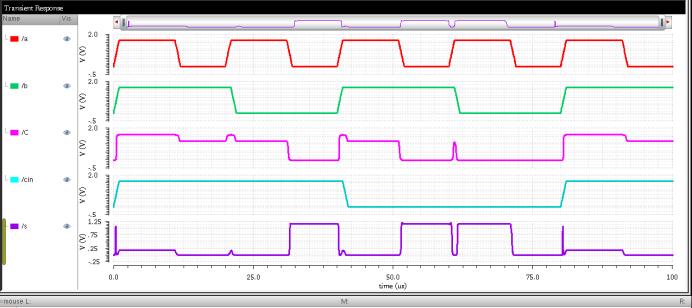
SimilartotheCMOSdesigningprocess,wehavedesigneda 64-BitPseudo-NMOS.ItisshowninFig-11.

The graph in Fig -10 shows the transient analysis of
withastoptimeof100us.
2.3
The Schematic shown in Fig -12 is designed using FullAdder equations with Transmission Gate Logic, and Transmission Gate 1-Bit Circuit is created as a symbol namedTransmissionGate1-BIT.Fig-13showsthesymbol ofthe1-BitTransmissionGate.
In Fig -12, A, B, and C are inputs and carry, sum areoutputs.
In Fig -13, V-pulse is connected to the inputs a,b, andcin individuallyand given voltage1 as0vand voltage2as1.8v
V-pulse for a, b and cin is provided with period 20us, 40us, 80us with pulse width 10us, 20us, 40usrespectively.
Vddisconnectedtotheground.
Using ‘DC Transient Analysis’, we simulated the circuit.


The graph in Fig -14 shows the transient analysis of TransmissionGate1-Bitwithastoptimeof100us
Fig-16:Peak-PowervalueandTotal-PowervalueofCMOS 64-Bitgraph

3.2 Power Analysis of Pseudo-NMOS 64-Bit


From the graphs in Fig -17, we can observe the TotalPowerandPeak-Powervalues
ThePeak-Powervalue: 23.49mw

TheTotal-Powervalue:23.77mw
SimilartotheCMOSandPseudo-NMOSdesigningprocess, wehavedesigneda 64-Bit TransmissionGate.It isshown inFig-15.

3.
3.1
From the graphs in Fig -16, we can observe the TotalPowerandPeak-Powervalues
ThePeak-Powervalueis:23.28mw
TheTotal-Powervalueis:23.77mw
Fig-17:Peak-PowervalueandTotal-PowervaluePseudoNMOS64-Bitgraph
3.3
FromthegraphsinFig-18,wecanobservetheTotalPowerandPeak-Powervalues.
ThePeak-Powervalue:4.17mw
TheTotal-Powervalue:46.34mw
3.2
Based on our design, the Table -1 shows that the CMOS logic family has the highest transistor count among the three options, while the Transmission Gate logic family has the lowest. However, the Transmission Gate logic family exhibits the highest peak power consumption, whilethePseudo-NMOSandCMOSfamilieshaveidentical power consumption characteristics. In terms of delay, all threelogicfamilieshavethesamevalueof107.608ns.The power-delay product (PDP) is the lowest for the TransmissionGatelogicfamily,indicatingbetterefficiency intermsofpowerconsumptionandperformance.
However, it may vary to different applications. We can choose the desired logic family based on cost, power, and performance.
4. CONCLUSIONS
Firstly, Transmission Gate Full-Adder circuits use fewer transistors than CMOS and pseudo-NMOS Full-Adder circuits. Secondly, Transmission Gate Full-Adder circuits also have lower delays than other logic families. Thirdly, TransmissionGateFull-Addersexhibitbetterpowerdelay product results than CMOS and Pseudo-NMOS Full-Adder circuits;however,thechoiceofthelogicfamilytobeused ultimately depends on the application's specific requirements, such as cost, power and performance. Hence, from our designs, these conclusions highlight the advantagesofusingTransmissionGateFull-Addercircuits in specific applications where power consumption and delayarecriticalfactors.
REFERENCES
[1] Ren,Y.,&Liu,Y.(2013).Anovelapproachtoimprove theperformanceofasynchronous circuitdesignusing self-timedcircuit.CiteSeerX,10.1.1.676.9601.
[2] Jampani, Y., & Gupta, G. B. (2022, July). Implementation of 1-Bit full adder circuit using pass transistor logic. IJRASET International Journal for Research in Applied Science & Engineering Technology, 10(7), 4974-4981. doi:10.22214/ijraset.2022.46097
[3] Trapti Mittal and Uma Sharma, “ANALYSIS OF FULL ADDER FOR POWER EFFICIENT CIRCUIT DESIGN”, IJARSEVol.No.4,Issue10,October2015
[4] Manjunath K M, Abdul Lateef Haroon P S, A. Pagi and Ulaganathan J, "Analysis of various full-adder circuits in cadence," 2015 International Conference on Emerging Research in Electronics, Computer Science and Technology (ICERECT), Mandya, India, 2015, pp. 90-97,doi:10.1109/ERECT.2015.7498994.
[5] Bhati, Ankita and Rita Jain. “Low Power DelayProductCMOSFullAdder.”(2015).
[6] G. R. Padmini, O. Rajesh, K. Raghu, N. M. Sree, C. ApurvaandK.saikumar,"DesignandAnalysisof8-bit ripple Carry Adder using nine Transistor Full Adder," 2021 7th International Conference on Advanced Computing and Communication Systems (ICACCS), Coimbatore, India, 2021, pp. 1982-1987, doi: 10.1109/ICACCS51430.2021.9441928.
[7] ZitongHan2021J.Phys.:Conf.Ser.1754012131
[8] Karunakaran,S.,&Poonguzharselvi,B.(2017,March). Exploration on power delay product of basic logic gates for various CMOS logic styles. International Journal of Engineering Studies, 9(2), 111-120. doi:10.11648/j.ijes.20170902.12
