
Study and Analysis of Low Power SRAM Memory Array at nano-scaled Technology
Sonali Verma1 , Dileep Kumar 21 Department of Electronics & Communication Engineering, Goel Institute of Technology and Management, Faizabad Road near Indira Canal Lucknow
2 Department of Electronics & Communication Engineering, Goel Institute of Technology and Management, Faizabad Road near Indira Canal Lucknow ***
Abstract - The cache memory design of microprocessors makes use of Static Random-Access Memory (SRAM) cells. Their efficiency is crucial because they are an integral part of the centralcomputer system. Only10–15 percent ofa modern system on a chip's (SoC) transistors are dedicated to logic, whereas the rest are used for cache memory, increasing the performance strain. On top of that, the AI-reliant nature of today's implantable, portable, as well as wearable electronic equipment highlights the needfor a robust SRAMarchitecture for CIM. Modernmobile communication devicesincludeample storage space for users' extensive media collections. Here, we adapt the Multi-thresholdCMOS designto create a low-power SRAM cell. Power usage andread/write cycleAccess Time can be lowered by using CMOS transistors with various threshold voltages. This work proposes a novel approach to reducing leakage in the idle state to cut down on power usage. The power usage of an SRAM cell is affected by the temperature, size of the transistors as well as the voltage used in the test. Data storage is an important function of several electronic components, specifically digitalones. The overallpowerusage of an SRAM is heavily influenced by leakage current. The research utilized a 1-bit 6T SRAM cell to construct a 1 KB memory array using CMOS technology and 0.6 volts for the supplyvoltage. Inthis section, we usedeepsubmicron(130nm, 90nm, and65nm) CMOStechnologyandthesix-transistor(6T) SRAM cell to analyze how varying topologies impact the performance of a 12T SRAM array.
Key Words: Cadence,SRAM,CMOS,7TSRAMCell,Leakage Power.
1. INTRODUCTION
Severalindustriesbenefitgreatlyfromartificialintelligence as well as machine learning [1]. Such techniques involve extensive data processing as well as calculation. ModificationstothehardwareexecutionofAItechnologies areessentialforenergy-efficientapplicationsliketheIoT[2] Oneofthemostpromisingapproachestoenhancingenergy efficiencyistheuseofin-memorycomputing.Multipleforms ofin-memory multiplication,aswell aslogical operations, are already a reality. Khwa et al. [3] to perform ternary multiplication, a six transistor (6T) cell was employed in conjunctionwithareferencevoltagegeneratingcolumn;Yin
etal.[4]aPMOSsubstrateoffsetona12Tcellproposedasa meansofproducingthesameeffect.Ontheotherhand,such techniquesneedmoreroomtoimplementthePMOSbody bias or a reference voltage-generating array. In addition, columns are used to store the operands for the aforementionedoperations [2][5][6][7],Itisnothowdatais stored in standard SRAM (static random-access memory), andhencenecessitatesextradatamovement.DRAMcellscan operate without a steady stream of electricity. However, DRAM relies on periodic pre-charging of its storage capacitors. Choi et al. DRAM array cells as well as a sense amplifier(SA)workedtogethertocompletethelogictasks [8].Alietal.aDRAMarraythatcan-dovectoraddition[9]. Yuetal.madeternarymultiplicationpossiblewitha4T2C DRAMchip[10].Yet,thereadoperationonmanyrowsmight lead to data corruption whenever IMC (in-memory computing) is implemented in DRAM. Therefore, this disadvantage necessitates the insertion of extra safety circuits.
2. LITERATURE REVIEW

Sudhakar Alluri et.al [11] In this study, we construct and simulatesix-transistorFINFET-basedstaticRAMcellsthen analyzethechallengesinherentintheirdesignaswellasthe metricsbywhichtheirsuccessismeasured.MinimizingSCEs, drastically reducing the maximum allowed duration, measuring the tremendous reliability of this process in a weak-power region, and so on. Power dissipation, leakage current,sub-thresholdcurrent,andstatic noisemarginfor FINFETandMOSFET6transistorstaticRAMwereevaluated at the 45nm node. While modern SRAM cells have greatly reducedpowerconsumptionaswellasleakagecurrent,the identicaltechniqueisutilized.TheperformanceofFINFETbasedSRAMcellshasbeenevaluatedtothatofconventional, advancedMOSFET-basedStaticRAMcells.
M.Srinivaset.al[12]Powerlossduringstandbyismostlydue toleakagecurrents,andtheyareunfortunatelyontherise. Sub-thresholdleakageincreasesasthethresholdvoltageis loweredbecausethegatecurrentleaksmorequickly.Asthe numberofpeoplewhorelyonmobiledevicesincreases,so doesconcernoverleakageenergyuse.Ifyourarelyuseyour phone and instead leave it in standby, you can improve
battery life by minimizing leakage power consumption. Therefore,reducingpowerusagehasgrownintoapriority duringtheCMOScircuitdesignprocess.AnANDgateusing theMOSparametermodel,designedandsimulatedin65nm CMOS technology at 27 0C, 0.70Vsupplyvoltage, provides confirmation of the proposed circuit. This is, of course, intendedtobesaidaloud.Powerlossduringoperationversus standby states, along with propagation time and dynamic dissipation, are contrasted with present MTCMOS and SCCMOSapproaches.
Hemant Kumar et.al [13] Against every reason in this research,weshowthat32nmSRAM(RL-SRAM)ispossible withAdd0.7VandRL-SRAMwithbodybias.Inreversible logic SRAM cells, the adiabatic approach allows the node capacitance energy to be utilized instead of dissipated as heat.OncomparingCNTFETRL-SRAMaswellasbody-biased RL-SRAM to CNTFET SRAM cells, we find that the former improves latency by 60.72%& the latter by 65.20%. The CNTFET SRAM cell design greatly enhances the average poweruse,leakagepoweranddelaytimedissipationwithout degradingtheoverallperformance,asshownbycontrasting itwithpriorwork.ButterflycurveaswellasN-curveanalyses areutilizedtobettercheckthelongevityofthememorycell.
S Pousia et.al [14] One of the most challenging issues in modern engineering is designing low-power, high-speed CMOS devices. Static power usage is becoming more of a problem as technology develops. Sleepykeeper technique, sleeptechnique,leakagecontroltransistortechnique,stack technique, & sleepy keeper leakage control transistor technique are only a few of the various approaches for reducing leakage power. Low power usage and fast speed were both possible in the CMOS design because to the suggestedpowergatingapproach.Inalow-power,fast-access design,thismethodisemployedtodeterminethehalfadder, x nor gate, x or gate, and 6T SRAM cell. SRAM cells save 35.9%ofpoweraswellas25.6%ofdelaycomparedtoahalf adder,whileanxorgatesaves19.5%ofpowerand33.5%of delay.Comparedtoastandardgate,NORgatereducesenergy consumption by 12.5% and delay by 23.2%. The leakage power consumption and simulation time are drastically decreasedusingTanner'sEDAtool.
HemantKumaret.al[15]Oneofthemostchallengingissues inmodernengineeringisdesigninglow-power,high-speed CMOS devices. Static power usage is becoming more of a problemastechnologydevelops.Thesleepmethod,thestack method,thesleepystackmethod,&thesleepyleakagepower strategyareonlyafewofthemanywaysavailable.Assilicon technologycontinuestoprogress,powerdissipationatthe NANO scale has emerged as a critical problem. A digital system's power consumption can be decreased while its performanceisincreased.Thisstudyevaluatestheoperation of several low-power CNTFET SRAMcells fabricated using Cadence Virtuoso 32 nm technology. Leakage Feedback, Sleep, Sleepy Keeper, Zigzag, & Stack are some of thelowpowerstrategiesusedbytheCNTFETSRAMcellinthisstudy.
Sleepy keepers have been shown to lower power consumptionbyasmuchas84.26%(81.13%)onaverage, 38.12%(43.01%) in delay, and 9.15%(20.80%) in leaky power consumption. The suggested CNTFET SRAM cells' memory cell stability is evaluated using a butterfly curve using an analytic N-curve method. Since the SRAM cell's performance indices improves considerably, increasing systemefficiencyevenascellsizegrows.
Shalini Singh et al. [16] SRAM memory was used for constructinga1KBmemory.A7TSRAMcellwithanaverage latencyof21nsandaminimalleakagecurrentof20.16pA wasusedtorealizethearraystructure.Thiswasachievedby employinga2DarrayconstructedfromtheSRAM'sbuilding blocks. The pre-charge circuit, sense amplifiers, address decoder, and write driver were all designed utilizing the CadenceVirtuosotoolin45nmtechnologytoaccommodate the32x32array.The1KBSRAM-relyingmemory'swriting, aswellasreadingoperations,consumed51.57mWand447.3 mWofpower,correspondingly.Reducingthenominalvoltage canhaveaneffectonthePVTfluctuations,thenoisemargin, andthecellstability.
Readstabilityorperiodicpre-chargeduringtheread/write cycle is a major challenge in SRAM design. This research detailedhowthenewSRAMdesigndevelopedbyAlexGong et al. [17], including a special emphasis on the reading operation,canaddressthesetwoproblems.Theutilizationof sense-amplifyingcellsallowed for the inversionofcellular nodes. It was hypothesised that by physically isolating the digitaloutputbitsfromthedataretentionelements,areadSNM-freeSRAMcellmightimprovereadresilience.Cadence design software was used to develop this in 0.18 m CMOS technology.ThetotalpowerusageofthisSRAMdecreased within similar operating settings as its conventional analogue.TheSRAMareaneededforthistechniqueisdouble thatof6TSRAMcellsor8transistorspercell.
Rashmi Bisht et al. [18] created an SRAM array & all its ancillary parts, including the sense amplifier, write driver circuit,rowdecoder,pre-chargecircuit.Noisewasreducedby employingdifferentialsensingamplifiers,whicharecapable of rejecting common mode voltage. Cross-coupled CMOS inverters were used to reduce the amount of static power lost. This design also features high noise immunity & low operatingvoltage.ThesuperiorstabilityofcompleteCMOS SRAM cells over resistive load SRAM cells at low supply voltageshavebeenestablished.Thetotal measuredpower draw of the SRAM array was 24.58 mW. The popular gpdk180library(alsoknownasthe180nmtechnologynode) wasusedduringthedesignprocess.
HimanshuBangaetal.[19]showedoffa16x16SRAMwith lesswastedspaceonthechipandlesswastedpowerfrom leakage. As a consequence, the SRAM's functionality improved.Thesmallerperipheralutilisedlesspowerbecause theconstraintsonitssizewereloosened.Thistechniqueis helpful forlow-energyapplications ifthe sizeof the SRAM
memory is not an issue. Significant reductions in power consumption were achieved by employing sleep & forced transistorapproachesinthisinvestigation.Comparedtothe sleepmethod,theforcedtransistorwasfoundtobe99.94% faster, and it also reduced overall power consumption by 56.92%.The16x16SRAMmemorywasdesigned,fabricated, andevaluatedusingtheCadencetoolandthebaselineUMC 180nmtechnologylibrary.
Improvingperformanceaswellaspowerconsumptionwhilst fixingtheproblemsofthestandardSRAMcell,ShyamAkashe etal.[20]createdafive-transistorSRAMcellwithzeroread staticnoisemargin.Theyusedthelargebiastowardszeroin thebitstreamofmemoryintypicalprogrammestodesign thisone-of-a-kindcellularstructure.Theprimaryresearch discoverythatinformedthisdesignwasthatcellleakageis quantified at the node wherein the transistor is disabled. Whencomparedtothe6TSRAMcell,theprojectedcellarea was 21.66%smaller while increasing speed by 28.57%, assumingidenticaldesignparameters.Thesuggestedcell's longevity,thatmimics45nmtechnology,wascalculatedwith theuseofproperread/writeoperations.Thenovelcellalso has70%shorterlatencythanaconventionalsix-transistor SRAMcell.Evenwhilethesuggestedcell'smemorycellaccess leakagecurrentdoubledforevery10degreesCelsiusabove roomtemperature,itwasstill72.10percentlowerthanthat ofthe6TSRAMcell.
3.
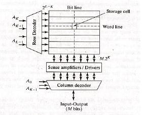
TheblockdiagramofatypicalSRAMhasdepictedinFigure.1. Bit-orientedandword-orientedlayoutsarebothpossiblefor SRAMs.Althougheachaddressinaword-orientedmemory typicallytakesupnbits(preferredchoicesofninclude8,16, 32,and64),whenusinganSRAMthatisbit-oriented,only onebitisneededforeveryaddress.Usingcolumndecoders orcolumnmultiplexers(YMUXs)directedtotheYaddress bits, two, four, or more columns can share a single sense amplifier.Itiscrucialtocreatearead-safeandwrite-reliable SRAMcell.Bothoftheserequirementsimposeoppositeones on the estimation of the transistors in an SRAM cell. The transistor ratios in an SRAM cell need to be calculated for optimal reading and writing. The preceding provides the basicsquaresforSRAMconstruction.
1. SRAMcell.
2. Pre-ChargeCircuit.
3. WriteDriverCircuit.
4. SenseAmplifier.
5. Rowdecoder.
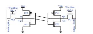
MemoryCellsThatUseSRAMFigure3depictsatypicalSRAM cell, which has six transistors. Q and Qb are the internal nodes that store the bit value and its complement, accordingly. These vertices are lifted by PMOS transistors PU1&PU2.PullingdowninternalnodesisthejobofNMOS transistors PD1 & PD2. The PG1 as well as PG2 pass transistorsallowforreadandwriteoperations.
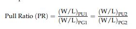
Hold,read,&writearethe3methodsofoperationavailable toanSRAMcell.Thecellretainsitsinternalbitvaluewhenin hold mode because the WL (wordline) signal is low. The bitlines (BL and BLB) are conditioned by an initial conditioningcircuitbeforeeveryreadorwriteoperation.The storedvaluecanberetrievedbyapplyingtheWLsignalto both PG transistors throughout the read operation. As a result, the PG and PD transistors discharge one of the BLs whereasanotherBLremainshigh.TheSRAMcellstoresthe bitaswellasitscomplementontheBLsinthisfashion.Fora PDtransistortobeabletodischargeaBL,itsmatchingPG transistorhastobeweaker.Therelativeefficiencyofthese transistors isseen byEquation (1).Forreadoperationsto succeed,CR values must be more than one. The capacitive valueofaBLishighbecauseitlinksmanyindividualcells.As a result, the discharge process is lengthy. Consequently, a sensing amplifier, that amplifies the comparatively small differentialvoltageacrosstheBLs,isusedtotransmitthebit valuetotheexternalcircuitry.
First, the value that is written upon the cell is used to determine which of the BLs will be pulled down by a powerful write driver. Since the design density has risen, morecapacitancehasbeenintroducedtotheWLassertion, makingitslower.Initially,aPUtransistorresistedtheBL's pullonthestoragenodeviaaPGtransistor.Thisimposesa ruleofthumbcalled"writeability."
4. 7T SRAM CELL: PROPOSED DESIGN
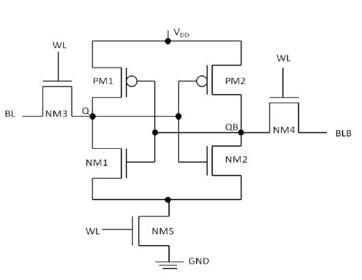
The7TSRAMCellisintroducedtohelpwithleakagecontrol. A schematic of a 7T SRAM cell is depicted in Figure 2. 7 transistorsareemployedinthisdesign,assuggestedbythe name.Likea6TSRAMCell,butwithanextraNMOStransistor connectingthepull-downtransistorstothegroundnode.WL istheinputoftheextraNM5transistor.Subthresholdleakage &gatetunnelingareprimarilycausedbyleakagecurrents.
Theleakagepowerisrelatedtothecell'scapacityforstorage. Whenthegatevoltageofatransistorislessthanitsthreshold voltage,asubthresholdcurrentisflowing.Thus,theNM3& NM4accesstransistorsaredisabledinstandbymodeifWLis assertedlow.Subthresholdleakagecurrentpassesthrough off transistors because of the stored value (logic 0) in the SRAM cell. It's possible that the supplementary bottom transistorNM5willseverthegroundconnection.Thislessens the likelihood of leaking occurring at the sources of SRAM cells. Bottom transistor NM5 switches on in active mode whenever WL is asserted high. Therefore, it functioned similarlytoa6TSRAMcellduringwriteandreadoperations. Themarginalgaininwriteaccesstimecausedbytheextra transistor is insignificant. However, the size of the array grows, especially for larger arrays. 7T SRAM cells have dimensionsthatarecomparableto6TSRAMcells,withthe NM5channelwidthat200nmandtheNM5channellengthat 120nmbothbeingtakenintoaccount.
4.1 Pre-charge Circuit
ThecoreofeachSRAMarrayisitspre-chargecircuit.Figure4 shows the charging circuit during the first stage of the process. Three PMOS transistors make up the pre-charge circuit.Thethirdtransistorperformsthepre-chargingduty, whereasthefirsttwoareusedforequalisation.
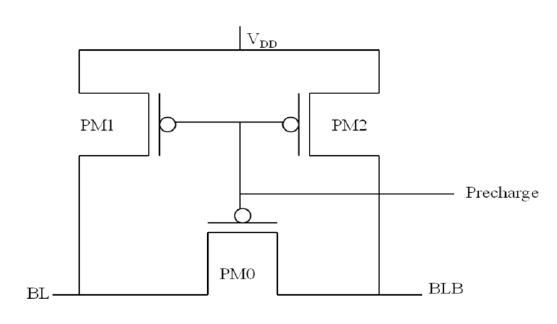
Before any read or write operations can take place, the bitlines must be pre-charged to VDD =0.7Vusing the prechargecircuit.PMOStransistorsarethoughttohaveawidth of200nmaswellasalengthof120nm.Inthearray,thereis onlyonepre-chargecircuitforeverycolumn.
4.3 Write Driver Circuit:
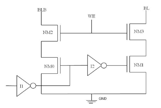
Discharging one of the bitlines is the main job of a write driver circuit. It is possible to activate the write driver by sendingaWriteEnable(WE)signaltoit.Eacharraycolumn justneedsasinglewritedrivercircuit.Figure3.3depictsthe writedrivercircuit.Ithas4NMOStransistors(NM0,NM1, NM2, &NM3) andtwo inverters (I1andI2).ForanNMOS transistor,120nmofchannellengthand200nmofchannel widtharetypicaldimensions.

4.2Sense Amplifier
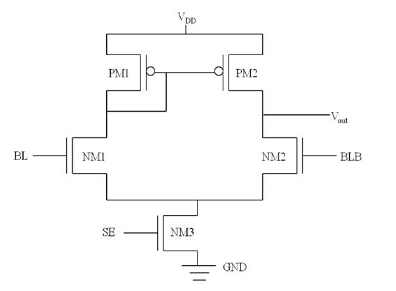
An SRAM without a sense amplifier would be useless. The schematicforaDifferentialTypeSenseAmplifier(DTSA)is
depictedinFigure3.4.Youmayknowitbetterbythename "voltagemodesenseamplifier."TheDTSAalgorithmoperates in a dynamic design mode, constantly monitoring the disparity among bitlines and adapting its output correspondingly.Asenseamplifier'sprimaryfunctionisto provide dependable performance throughout a read operation;henceitmustbeabletowithstandinternalsystem noise without being affected. Several variations of sense amplifiers have been described in academic papers. DTSA outperforms other sensing amplifiers and is immune to systemnoise.Theactivecurrentmirrorload(PM0&PM1)is comprisedofadifferentialpair(NM1andNM0)andabiasing currentsource(NM2).ThedrainofeithertheNM0orPM0is linkedtothebitlines,whiletheinputisthedifferentialpair.A SenseEnable(SE)signalactivatestheSenseAmplifierduring areadoperation.
4.4 Row/Column Decoder
Addressdecodersservetotranslateauser'sinputtedaddress intoaroworcolumnactivationinamemorylayout.Toaccess a specific WL or WE in an SRAM array, a row & column decoderisemployed.
Theblockdesignofadecoderwith4inputs(a,b,andc)and eightoutputs(X0throughX7)isdepictedinFigure3.5.This studyemploysadecoderbuiltonanANDgate.
5. CONCLUSIONS
Allcurrenthigh-performanceVLSIcircuitsnecessitatesome sortofdatastoragesolution.Today'sbusinessesrequirethe abilitytostoreaswellasretrievemassiveamountsofdata quickly.Themaximumretentionperiodisclosetotwoyears, makingitpossibletoruntheprogrammeagain.UsingCMOS technology, this work examines a 1 KB SRAM array in bit orientation,rangingfrom6TSRAMcellsto12TSRAMcells. Ithasa storage capacityof 1024bits.Thesuggested 1 KB SRAM memory array is considered low leakage, has small feature sizes, with low power consumption. Taking into accountallofthevariables,itwasfoundthatthe1KB-SRAMbasedmemory'spowerusagevariedsignificantlybetween theread&writeoperations.Thenumberofbitsofdatathat may be stored in a given area is a crucial metric for any storagesystem'sefficiency.Memoryaccesstimeisanother crucial indicator of performance. The speed of a memory arrayissetbyitsaccesstime.Itispossibletolessenpower consumption & delay by using CMOS transistors with varying threshold voltages. This work proposes a novel strategy that minimizes leakage current in the idle state, hencedecreasingpowerusage.WhentestinganSRAMcell, theamountofpowerusedishighlydependentonthevoltage provided,theoperatingtemperature,andthetransistorsize. Informationmaybestoredinthememoryofmanyelectronic components,particularlydigitalones.Powerconsumptionin SRAMismostlydrivenbyleakagecurrent.Inthispaper,a1 KBmemoryarraywasconstructedutilisinga1-bit6TSRAM celland0.6voltsofsupplyvoltageusingCMOStechnology. The various possible combinations are displayed below. Here, we examine the performance of a twelve-transistor (12T) SRAM array versus a six-transistor (6T) SRAM cell implementedindeepsubmicron(130nm,90nm,and65nm) CMOStechnologies.
REFERENCES
[1] A. Biswas and A. P. Chandrakasan, “CONV-SRAM: An energy-efficient SRAM with in-memory dot-product computation for low-power convolutional neural networks,” IEEE J. Solid-State Circuits, 2019, doi: 10.1109/JSSC.2018.2880918.
[2] H.C.Chen,J.F.Li,C.L.Hsu,andC.T.Sun,“Configurable 8TSRAMforEnblingin-MemoryComputing,”2019.doi: 10.1109/ICCET.2019.8726871.
[3] X.Si et al.,“ADual-Split6TSRAM-BasedComputing-inMemory Unit-Macro with Fully Parallel Product-Sum Operation for Binarized DNN Edge Processors,” IEEE Trans. Circuits Syst. I Regul. Pap., 2019, doi: 10.1109/TCSI.2019.2928043.
[4] S.Yin,Z.Jiang,J.S.Seo,andM.Seok,“XNOR-SRAM:InMemory Computing SRAM Macro for Binary/Ternary Deep Neural Networks,” IEEE J. Solid-State Circuits, 2020,doi:10.1109/JSSC.2019.2963616.
[5] X.Sun,R.Liu,X.Peng,andS.Yu,“Computing-in-Memory with SRAM and RRAM for Binary Neural Networks,” 2018.doi:10.1109/ICSICT.2018.8565811.
[6] S.Jeloka,N.B.Akesh,D.Sylvester,andD.Blaauw,“A28 nmConfigurableMemory(TCAM/BCAM/SRAM)Using Push-Rule6TBitCellEnablingLogic-in-Memory,” IEEEJ. Solid-State Circuits, 2016, doi: 10.1109/JSSC.2016.2515510.
[7] M.Kang,S.K.Gonugondla,A.Patil,andN.R.Shanbhag, “A Multi-Functional In-Memory Inference Processor Using a Standard 6T SRAM Array,” IEEE J. Solid-State Circuits,2018,doi:10.1109/JSSC.2017.2782087.
[8] H.Choi,Y.Lee,J.J.Kim,andS.Yoo,“ANovelIn-DRAM Accelerator Architecture for Binary Neural Network,” 2020.doi:10.1109/COOLCHIPS49199.2020.9097642.
[9] M.F.Ali,A.Jaiswal,andK.Roy,“In-MemoryLow-Cost Bit-Serial Addition Using Commodity DRAM Technology,” IEEE Trans. Circuits Syst. I Regul. Pap., 2020,doi:10.1109/TCSI.2019.2945617.
[10]C.Yu,T.Yoo,H.Kim,T.T.H.Kim,K.C.T.Chuan,andB. Kim,“ALogic-CompatibleeDRAMCompute-In-Memory withEmbeddedADCsforProcessingNeuralNetworks,” IEEE Trans. Circuits Syst. I Regul. Pap., 2021, doi: 10.1109/TCSI.2020.3036209.
[11]S.Alluri,B.Balaji,andC.Cury,“Lowpower,highspeed VLSI circuits in 16nm technology,” 2021. doi: 10.1063/5.0060101.
[12]M.SrinivasandK.V.D.Sagar,“AnalysisonPowerGating CircuitsBasedLowPowerVLSICircuits(BCDAdder),”
2021.doi:10.1088/1742-6596/2089/1/012080.
[13]H.Kumar,S.Srivastava,andB.Singh,“Lowpower,highperformancereversiblelogicenabledCNTFETSRAMcell with improved stability,” 2019. doi: 10.1016/j.matpr.2020.06.475.
[14]S.PousiaandK.Murugan,“VLSIImplementationOfHigh Speed Low Power Design Using Hybrid Power Gating Technique,” IOP Conf. Ser. Mater. Sci. Eng., 2021, doi: 10.1088/1757-899x/1084/1/012058.
[15]H.Kumar,S.Srivastava,P.K.Khosla,andB.Singh,“High Stable and Energy Efficient Emerging Nanoscale CNTFET SRAM Cells using Circuit Level Low Power Techniques,” Silicon, 2022, doi: 10.1007/s12633-02101581-8.
[16]S. Singh and S. Akashe, “Low Power Consuming 1KB (32×32)MemoryArrayUsingCompact7TSRAMCell,” Wirel. Pers. Commun.,2017,doi:10.1007/s11277-0174226-z.
[17]C.A.Gong,C.Hong,K.Yao,andM.Shiue,“ALow-Power Area-EfficientSRAMwithEnhancedReadStabilityin0. 18-µmCMOS,”pp.729–732,2008.
[18]R.Bisht,P.Aggarwal,P.Karki,andP.Pande,“Lowpower and noise resistant 16×16 SRAM array design using CMOSlogicanddifferentialsenseamplifier,”2017.doi: 10.1109/CCAA.2016.7813954.
[19]H. Banga, “Implementation of 16x16 SRAM Memory Array,” 2017 Int. Conf. Recent Innov. Signal Process. Embed. Syst., pp. 458–462, 2017, doi: 10.1109/RISE.2017.8378199.
[20]S.Akashe,S.Bhushan,andS.Sharma,“Highdensityand low leakage current based 5T SRAM cell using 45 nm technology,” 2011. doi: 10.1109/ICONSET.2011.6167978.
[21]K.Takeda et al.,“Aread-static-noise-margin-freeSRAM cell for low-VDD and high-speed applications,” IEEE J. Solid-State Circuits, 2006, doi: 10.1109/JSSC.2005.859030.
[22]L.Chang et al.,“StableSRAMCellDesignforthe32nm NodeandBeyond,”pp.128–129,2005.
[23]T.W.Oh,H.Jeong,K.Kang,J.Park,Y.Yang,andS.O.Jung, “Power-Gated9TSRAMCellforLow-EnergyOperation,” IEEE Trans. Very Large Scale Integr. Syst., 2017, doi: 10.1109/TVLSI.2016.2623601.
[24]I.J.Chang,J.J.Kim,S.P.Park,andK.Roy,“A32kb10T sub-threshold sram array with bit-interleaving and differentialreadschemein90nmCMOS,” IEEE J. SolidState Circuits,2009,doi:10.1109/JSSC.2008.2011972.
[25]Y.He,J.Zhang,X.Wu,X.Si,S.Zhen,andB.Zhang,“AHalfSelectDisturb-Free11TSRAMCellWithBuilt-InWrite/ Read-AssistSchemeforUltralow-VoltageOperations,” no.1,pp.1–10.
[26]J. Sun and H. Jiao, “A 12T Low-Power Standard-Cell BasedSRAMCircuitforUltra-Low-VoltageOperations,” 2019.doi:10.1109/ICICDT.2019.8790912.