A Comparative Performance Analysis of Copper on Chip and CNTFET
Nano Interconnects
Arun Kundu1, Manoj Kumar2Abstract – The digital electronics industry has advanced quickly, which has led to the miniaturisation of semiconductor industries. Power consumption in the Deep Sub Micron domain has become a significant problem due to leakage current, hence researchers are always looking at different strategies to reduce it. There are other approaches available for the same thing, and using carbon nanotube technology is one of the methods that shows promise for effectively designing low power circuits. In this article, new methods for reducing leakage power are introduced. In this work, the primary performance metrics of the CNTFET and the Copper on Chip Nano-interconnect have been compared. By combining process variation in CU and CNTInterconnects with tube variation at 32nm technology, we were able to quantify the effects of ION and IOFF current. We also examined how the performance of digital circuits changed as technology advanced. The various simulation results show that applying 10% deviation from the mean to various device characteristics parameters, including source and drain doping concentration with Cu and CNTFET interconnects for NFET and PFET with a range of tubes from 1 to 16, is effective. These parameters include length of gate (L-Tube), width (WTube), threshold voltage (Vth), thickness (total), and source&drain doping concentration. All of the experimental results were obtained using the HSPICE simulator and the 32nm Berkley Predictive Technology module with the CU and CNT SPICE models at 27 °C temperature.
Key Words – ION and IOFF, CNTFET, Mean, Standard Deviation, Power Consumption.

1. INTRODUCTION
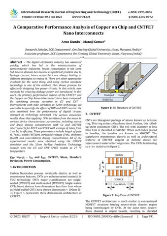
Carbon Nanotubes possess invaluable electric as well as monotonousfeatures.CNTsareanInterconnectmaterialin VLSI technology. CNTs major classifications are singlewalled(SWCNT)andmulti-walled(MWCNT).Single-walled CNTs baseddevices havedimensions less than1nm where asMulti-walledCNTs have devicedimensions<100nm[13]. Figure 1 represents three dimensional architecture of CNTFET.
CNTs are Hexagonal package of atoms known as benzene ring.ThisringmakesaGraphenesheet.Further,thisrolledup sheet constitutes CNTs. The roll with diameter of less than 1nm is classified as SWCNT. When such tubes placed in bundles, the bundles are known as MWCNT. The superlative monotonous electric as well as architectural features of CNTFET suggest as definite choice for Interconnectmaterialforlongterms.TheCNTsfunctioning can be statedasinfigure2.







The CNTFET architecture is much similar to conventional MOSFET structure barring source-drain channel region being interchanged by CNTs. At the same time, sourcedrain channel is doped heavily, resulting in elevated

operating speed [4-5]. The inbred CNTs are manufactured circumambient flat metallic gate terminal havinghigh-k constant dielectric strength as zirconium oxide (ZrO2) and hafnium oxide (HfO2). The under layer is completely masked with non-conducting husky Silicon-oxide slab. A heterogeneousCNTFETaqueductisconstructedwithinfuse significant numbers of nanotubes lined straight along the widthofchannel,insucharrangementcentretocentregap inneighboringtubesisknownaspitch.
While simulating the CNT Source-Drain are doped by 0.78%,havingHfO2asgatenon-conductingmaterialhaving thickness 3nm as well as SiO2 clot having concentration 10µm [6-8]. CNTs have a feature i.e. energy bandgap, ���� is oppositely harmonious to bore size, hence allowing waveringofbandgapwiththeCNTsdiameter[9-10].
ThefeaturesofCNTFETsare:-
Arrangement of carbon atoms in CNTs possessing unparalleledfeatures:
Electric features: It is having better conductivity of both metallicaswellassemiconductingfeatures.
Elasticity feature: Graphene sheet is constituted by Carbon atoms with durable bonding. The elasticity is greateraspressedtheCNTisbentbutreturnstonominalif forcereleased.
Thermal Conductivity: CNTFETs have much greater conductivity as C-C chemical bond providing much needed potency and firmness to counter strains. Greater thermal conductivity has greater scope in nano scale molecular sensingdevices.AlsoCNTsareprominentelectionasmade by its features flimsy weight, litheness superior electro mechanicalfeatures.
3. INTERCONNECTS
An Interconnect has linear as well as non-linear components such as RLC of figure 3 for discerning developmentproceduresmodelingofnecessarydemeanor. Here Cu is countered against CNTFETs Interconnects posing enormous scope for performance existing conditions[10-12].
As figure 4 shows three dimensional sight for Cu Interconnects, for thequantification with centres Cu Interconnect along middle line to earth armanent is dsg anddgg CNT.





4. RESULTS AND DISCUSSIONS
Simulation results of 1, 4, 8, 16 CNT Interconnects suggest 11.05% deviation from WFF as average magnitude poses IOFFcurrentclose to 112% has Tube-1 and 160% for Tubes 4, 8, 16 this gives greater mean regulation of IOFF Tubes fluctuations in domains that 9% of average magnitude for alonglengthexhibits43.09%,Rangewideexhibits37.88%, altitude 7.33%, WFF 115%, T-Tube depicts 38%, N have 34%sequentialmeanrangefluctuationinIOFF.Itconcludes Tubes and feature deviation exhibit larger IOFFfluctuations incomparisontoION.
in Cu
latency about 77% as well as percolation energy consumptiondiminishes87.88%aswhilethescalingdown device dimensions, smaller VDD as well as entangled manifolds vector set, while as well various concerns reducing for retain identical electric field having maintain latest techniques, design developments and latest and recent EDA setup, with capabilities for handling issues pertaining to most recent fabrication methods including deviationdemands.
REFERENCES
1. Dadoria,A.K.,Khare,K..:DesignandAnalysisofLow Power Adiabatic Logic Circuits by Using CNTFET Technology, Circuit System and Signal Processing, Springer, 38(2),1-19(2019).
2. Dadoria, A.K., Khare, K; Gupta, T.K; Panwar U.: “Integrating Flipped Drain and Power Gating Techniques For Efficient FinFET Logic Circuits”, International Journal of Numerical Modelling: Electronic Networks, Devices and Fields., JohnWiley, 31(1),1-8(2018).
3. Chandel, R; Kumar, A.: Design and Development of Dielectric based Electrostatic Micro actuators IETE Journal of Research Taylor & Francis, 46(4), 261-264 (2000).
4. Jadav, S; Vashistah, M; Chande, R.: RLC equivalent RC delay model for global VLSI interconnect in current mode signalling, International Journal of Modelling and Simulation, Taylor & Francis, 35(1), 27
34 (2015).
5. Stanford University CNFET Model.: (2014). http://nano.stanford.edu/model.php?id=23
Figure7 depicts leaking losses energydissipation covering regulation yardstick criterion circuits comprising from Cu as well CNTFET Interconnects to agreement with affirmation of outcomes. Concluding Cu Interconnects dissipate larger energy as compared to C17 (ISCAS 85) conserves close to 46.86%, while B01 (ITC99) 40.9%, B02 (ITC99)48.9%andB06(ITC99)53.02%.
5. CONCLUSION
An idiosyncratic resemblance of Cu with CNTFET Interconnects for optimization has outcomes exorbitantly diminution of power dissipation. This work is suggesting PVTfluctuationsofvariousfeaturesatelevatedfrequencies with diminished energy Interconnects usage. P-CNTFETs possessmoreofVth,withscalingofcurrentleakagewhilein futile idle phase. The outcome study suggests the CNT InterconnectscoupledbyCNTFETmodelsconsumeenergy more economically. CNT-Interconnect sustains ever changing energy about 90%, cuts down transmission
6. HSPICEvA-2008.03.: (2014). http://www.synopsys.com/Community/Interoperabil ity/HSPICE
7. Predictive Technology Model.: (2014). http://ptm.asu.edu
8. Castro C, John; Pulfrey, DL.: Carbon nanotube transistors:anevaluation.ProceedingsofSPIE:Device and Process Technologies for MEM's, Microelectronics, and Photonics III. Bellingham, Washington,USA; 5276,1-10(2004).
9. Khursheed, A; Khare, K; Haque, F.Z.: Designing highperformance thermally stable repeaters for nanointerconnects. Journal of Computational Electronics, Springer, 18,53-64,(2019).
10. Pasupathy, K.R; Bindu, B.: Low power, high speed carbon nanotube FET based level shifters for multi-
VDDsystems-on-chips. Microelectron Journal. 46, 1269-1274(2015).
11. Girish Kumar, M; Chandel, R; Agrawal, Y.: An Efficient Crosstalk Model for Coupled Multi-Walled Carbon Nanotube Interconnects, IEEE Transactions on Electromagnetic Compatibility, 60(2), 487–496 (2018)
12. Iijima, S.: Helical microtubules of graphitic carbon. Nature;354(6348),56-58(1991)