Performance analysis of NOR CAM cell using CMOS-HP, CMOS-LP and FinFET 16nm technology
Vasundhara Patel K.S2Abstract - Content addressable memory (CAM) is used in 
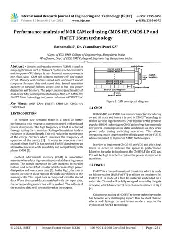
many applications such as Network routers, Cache controllers and low power CPU design. It searches total memory array in one clock cycle. CAM cell contains memory cell and match circuit. Memory cell contains stored data and match circuit compares the input data and stored data. Search operation happens in parallel fashion, access time is less and power dissipation will be more. This paper presents functionality of NOR based CAM cell implemented using CMOS-LP, CMOS-HP, FinFET 16nm technology and power reduction in HSPICE tool.
Key Words: NOR CAM; FinFET; CMOS-LP; CMOS-HP; HSPICEtool
1.INTRODUCTION
In present day scenario there is a need of better performancewithrespecttoincreaseinspeedwithreduced powerdissipation.Thehigh frequencyofCAMisachieved throughscalingthetransistors.Scalingoftransistorsleadsto reductioninchannellength.Thiswillreducethetransittime of the charge carriers which increases the frequency of operation of the device [1]. In order to overcome short channeleffectsFinFETshasevolved.FinFETshasbecomean alternativebecauseofitsscalabilityandcompatibilitywith planarCMOS[2].
Content addressable memory (CAM) is associative memorywheredataisgivenasinputandaddressisgivenas output. The search operation in CAM happens in parallel fashionand henceCAMisfaster whichcauseshighpower dissipationandlessaccesstime[3]. IntheFig1,thedatais senttothesearchdataregisterthroughsearchlinestothe memorycells.Thisinputdataiscomparedwiththestored data.Whenthestoreddataismatchedwiththeinputdata, thecorrespondingmatchlinewillbeenabled.Theaddressof thematcheddatawillbeconsideredastheoutput.
1.1 CMOS
BothNMOSandPMOShassimilarcharacteristicsduring onandoffstateandhenceitisusedinCMOSTechnologyto realizevariouslogicfunctions.OverBipolarortheprevious popularNMOStechnologiesCMOStechnologyhasextremely low power consumption in static conditions as they draw power only during switching operation. This allows integratingmuchlargernumberoflogicgatesontheVLSIIC whencomparedtoBipolarorNMOStechnologies.
InordertoimplementCMOS-HPtheVDDandVthiskept lower in order to improve the speed in performance. Likewise,inordertoimplementtheCMOS-LPtheVDDand Vthwillbehighinordertoreducethepowerdissipationin transistor
1.2 FINFET
FinFETisathree-dimensionaltransistorwhichismade onSiliconwafers(BulkFinFET)orsilicononinsulator(SoI FinFET). It is made of a thin fin material embedded on a substrate.Channelwillbefullywrappedaroundbythegate ofdevice,whichhavecontroloverchannelasshowninFig2 [4].
ContinuousscalingofMOSFETtolowertechnologynodes hasbecome verychallengingaspect. Due to short channel effects and leakage current issues made a way to the evolutionofFinFETtechnology.
Most widely used operating modes of FinFET are explained below. FinFET structure consists of two gates namely,frontend(G1)andbackend(G2)asshowninFig3.
When there is a match in D and SL disables the pulldown pathandMLremainsinVDD[5].
Theareaconsumptionismoreandthefrontgateandthe backgateareoperatedindividually.
Theswitchingspeedismoreandithasgoodresistance whencomparedtoothermodes,asboththefrontandback gatesareshorted.
Inthereversebiasmode,inordertosuppresstheeffects ofsubthresholdleakagecurrentthebackgateofFinFETis associatedtoareversebiasvoltage.
A CAM is a special type of memory device which implementsalook-uptablefunction.ACAMisclassifiedinto twotypes,binaryCAMandternaryCAM.
Binary CAM will cache only ‘0’ and ‘1’. It is used in applications which need exact match between the stored data and input data. Table1 represents truth table of the BCAM
ACAMcellhastwobasicfunctionalities:storingabitin SRAMandcomparisonofabit.NOR-typeCAMcellisshown inFig5.Thecomparisonbetween andDwhicharestored inmemory,andthesearchdataissentonthesearchline andSL.ByusingdynamicXNORlogiccomparisoncircuitthe outputisdrawnfrommatchlineML.ThemismatchofDand SL activates the pulldown path, connects ML to ground.
Ternary CAM stores three states ‘0’, ‘1’ and ‘X’. The ‘X’ state is additional state referred to as the “mask bit” or “don’tcarebit”.TCAMisusedforapplicationsforbothexact andpartialmatches.Table4representstruthtableforTCAM [6].
4. WORKING
Fig 5. shows SRAM based BCAM cell using XNOR transistorlogiccircuit.Thedataisstoredandreadsimilarto SRAMatnodeVxwhilesearcheddataissenttolinesSLand SLB. When there is a mismatch between stored data and searcheddata,matchlinevoltageisdischargedtoGNDand mismatchedoutcomeispresented.
Fig 6. shows SRAM based TCAM with XNOR transistor logic circuit as a compare circuit, where data is stored in nodeVxatSRAM1andVyatSRAM2.
Fig 7. shows SRAM based BCAM cell using XNOR transmissiongatelogiccircuit.TheCAMoperationhappens thesameasdiscussedinprevioussections.InBCAMXNOR transistorlogic,thetransistorcountismoreaswecanseein Fig 5. Thus, transistor XNOR logic circuit is replaced with transmissionXNORlogiccircuitinmatchcircuit.Fig8.shows SRAM based TCAM with XNOR transmission gate logic circuit.
Fig9.showsSRAMbased BCAMcellusingXNORswitch stacklogiccircuit.TheoperationoftheCAMcellisdiscussed in the above section. In previous section 1.b. the power dissipation is more. Hence in this section the proposed circuitreducesthepowerdissipation.Theworkingofthis circuitisunderstoodwiththehelpofthetruthtable.Fig10. showsSRAMbasedTCAMwithXNORtransistorlogiccircuit.
5. RESULTS AND SIMULATION
AlltheCAMoperationsisperformedin16nmtechnology byusingCMOS-LP,CMOS-HPandFinFET.Poweranddelay valuesarecomparedforeachofthecircuitdescribedabove
Bycomparingtheobtainedvalues,wecanseethatthere is 15% - 19% reduction in power dissipation in FinFET BCAMwhencomparedothercircuits.19% -25%ifpower dissipationinreducedinFinFETTCAMwhencomparedwith othercircuits.
From the obtained delay values, there is 20% - 24% reductionofdelayinFinFETBCAMwhencomparedother circuits.Around27%-37%ofreductionindelayisseenin FinFETTCAMwhencomparedtoothercircuits.
6. CONCLUSIONS
ThisprojectexplainsthedesignandworkingofCAMwhich consists SRAM as memory cell and XNOR as comparison circuit.Byadoptingdifferenttechnologies,theperformance of BCAM and TCAM are investigated. The CAM operations are carried out by using CMOS-LP, CMOS-HP and FinFET technology and obtained power and delay values are compared for different compare circuit. From the experiment, FinFET CAM cells with XNOR switch stack circuitgivesbetterperformancewithlesspowerdissipation anddelaywhencomparedtootherlogiccircuitsinall the technologynodes
REFERENCES
[1] Kostas Pagiamtzis, Student Member, IEEE, and AliSheikholeslami, SeniorMember, IEEE, “Content addressablememory(CAM)circuitsandarchitectures:A tutorial and survey”, IEEE JOURNAL OF SOLID-STATE CIRCUITS,VOL.41,NO3,MARCH2006
[2] Tasneem Salam H et all, “A comparative performance analysis of CAMs using different model files in Spice”, 2017 International Conference on Nextgen Electronic Technologies, 978-1-5090-5913-3/17/$31.00 c 2017 IEEE,pp191-193
[3] ATernaryContent-addressableMemoryBasedonFully Depleted Silicon on Insulator, M. Tech report VLSI DesignandEmbeddedSystems,BMSCE,2019
[4] Harshit Agarwal et all, “Designing 0.5 V 5-nm HP and 0.23 V 5-nm LP NC-FinFETs With Improved IOFF Sensitivity in Presence of Parasitic Capacitance, IEEE TRANSACTIONSONELECTRONDEVICES,VOL.65,NO. 3,MARCH2018,pp1211–1216
[5] Nitin Mohan, Low-Power High-Performance Ternary Content Addressable Memory Circuits, Ph.D. thesis, UniversityofWaterloo,Ontario,Canada,2006
[6] Meng-ChouChangetall,“DesignofAsymmetricTCAM (Ternary Content Addressable Memory) Cells Using FinFET”,2014IEEE3rdGlobalConferenceonConsumer Electronics (GCCE) 978-1-4799-05145-1/14/$31.00 ©2014IEEE,358-359
[7] AmeerM.S.AbdelhadiandGuyG.F.Lemieux“Modular SRAM-based Binary Content Addressable Memories” 2015 IEEE 23rd Annual International Symposium on FieldProgrammableCustomComputingMachines.
[8] Bhuvana R.1 et all, “Content Addressable Memory performance Analysis using NAND Structure FinFET”, GlobalJournalofPureandAppliedMathematics.ISSN 0973-1768 Volume 12, Number 1 (2016), pp. 10771084
[9] B. -D. Yang and L. -S. Kim, “A Low-Power CAM Using Pulsed NAND
NOR Match-Line and Charge-Recycling Search-LineDriver,”IEEEJ.Solid-StateCircuits,vol.40, no.8,pp.1736–1744,Aug.2005.
[10] Vijayalakshmi et all, “Content Addressable Memory UsingXNORCAMMatrix”,InternationalConferenceon CommunicationandSignalProcessing,April6-8,2016, India,
[11] PRIYANKA PAWAR et all, “HIGH SPEED AND LOW POWER CMOS TECHNOLOGY BASED RAM-CAM MEMORY DESIGN”, International Research Journal of
EngineeringandTechnology(IRJET)Volume:03Issue: 05May-2016pp1199–1202
[12] DejanGeorgiev,“LOWPOWERCONCEPTFORCONTENT ADDRESSABLE MEMORY (CAM) CHIP DESIGN”, InternationalJournalofAdvancedResearchinElectrical, Electronics and Instrumentation Engineering Vol. 2, Issue7,July2013
[13] Rahul Nigam and Santosh Pawar, “A Power Efficient Improved NOR-Type TCAM Design using OR-Type Match-Line Segment”, International Journal of Recent TechnologyandEngineering(IJRTE)ISSN:2277-3878, Volume-8Issue-6,March2020,pp4885–4890
[14] Y.-J.ChangandY.-H.Liao,“Hybrid-TypeCAMDesignfor Both Power and Performance Efficiency,” IEEE Trans. VeryLargeScaleIntegr.(VLSI)Syst.,vol.16,no.8,pp. 965–974,Aug.2008.
[15] A.T.Do,C.Yin,K.Velayudhan,Z.C.Lee,K.S.Yeo,andT. T.Kim,“0.77fJ/bit/searchContentAddressableMemory Using Small Match Line Swing and Automated BackgroundCheckingSchemeforVariationTolerance,” IEEEJ.Solid-StateCircuits,vol.49,no.7,pp.1487–1498, Jul.2014