International
Research Journal of Engineering and Technology (IRJET)

Three Phase Seven-level Triple Voltage Booster Switched-Capacitors based Multilevel Inverter with Minimum Components
Vikram Singh Sehmi1 , Dr. Nagendra Tripathi21M.Tech. Student, Department of Electrical Engineering, Bhilai Institute of Technology, Bhilai (C.G.), India
2Professor, Department of Electrical Engineering, Bhilai Institute of Technology, Bhilai (C.G.), India ***
Abstract: This research proposes an economically feasible 3-phase triple-gain switched-capacitor (SC) multilevel inverter (MLI) configuration. The proposed structure has one source and uses the fewest switching components possible to produce an output voltage waveform with seven levels from line to line. The newly proposed SCMLI configuration features a built-in capacitor voltage balancing capability and uses two switching capacitors per phase leg. Level shift pulse width modulation approach, operating theory, and structural description have all been discussed. To demonstrate the merits of the proposed work with the existing topologies, a fair comparison study has been provided. The simulation results show that the proposed SCMLI configuration is feasible and has been verified theoretically.
Keywords: Three Phase Multilevel Inverter; Seven Level MLI; Economically Feasible Inverter Design, SCMLI.
1. Introduction
Thepopulationandindustrializationareexpandingquickly,whichincreasestheusageoftraditionalenergysources andgreenhousegasemissions[1].Therehasbeenalotoffocusonsustainableenergysourcesasawaytoslowdownthe rateatwhichconventionalenergysourcesareusedup.However,electricityisproducedbyavarietyofrenewableenergy sources, including solar photovoltaic, wind, and fuel cells. Solar and wind are the most widely used renewable energy sourcesduetotheiraccessibility,environmentalfriendliness,andimprovementsinpowersemiconductortechnology Due tothe relatively low output power from this source, it will not meet the requirements for power qualityfor applications likeelectricandfuel cellvehicles,gridconnections,andindustries.Asa result,a transformeror boostconvertermustbe usedtoincreasetheoutputvoltage.Theuseofthetransformermakesthesystembigandexpensive. Anextensiveamount ofstudyhasbeendoneontheconvertertoincreasetheoutputvoltage. Amongtheseconverters,multilevelinvertersare essential for power conversion owing to improved power quality, enhanced performance, and low, medium, and highpowerapplications.
International Research Journal of Engineering and Technology (IRJET)

minimizecurrent spikes. A nine-level single-sourcedesign builton theSC principle issuggested inthearticle[23],but it has fewer components than traditional topologies. The amount of parts required to reach the appropriate level is still considerable, though. In order to accommodate the extra switches, driver circuitry must be added, which raises the system's cost and increases power loss. Neutral Point Clamped Inverters (NPCI), which generate three-level alternating current(AC)outputinasinglestage,arerecommendedforusageinboostingDCvoltagetotherequiredlevel[24,25].In thearticle[26],designingasinglephasehybridmultilevelinverterforastandalonesystemthatproducesthreelevelsofTtypelegandthreelevelsofdiodeclampedlegusingasymmetricalvoltageinputsourcesisdiscussed.
The majority of topologies, it has been shown through a survey of the literature, have a number of demerits, including increased power devices, high voltage stress across the switches, low voltage gain, and absence of enhancing ability Therefore, the ideasin the aforementioned statements have been employed to developthe alternative SC-based inverter configuration that isdiscussed in theproposed work Thefollowingare the primarycharacteristicsof the recommended topology:
a) Themagnitudeofthevoltageboostingcapabilityisthree.
b) Theinbuiltabilityofcapacitorstobalancetheirvoltages.
c) Itdecreasedthenumberofswitchingcomponents.
d) Useofasinglesource,
e) Onlyabout50%ofswitchingpartsarefunctionalatanyvoltagelevel.
2. The Proposed 3-Ф SCMLI Topology A. Circuit Description
The3-ФSCMLIstructuraldesignisdepictedinFigure1.Sixpowerswitches(SXi i.e.,1,2,...,6)areusedineachphase leg,togetherwithapowerdiode(DX),twocapacitors(CX1 andCX2),andasingleDCsource,whereX thephase(R,Y,B). Any renewable energy source or battery can provide power to this voltage source. The proposed SCMLI can produce a seven-levelvoltagewaveformacrosstheloadendswhentheline-to-linevoltageistakenintoaccount(0,+1VDC,+2VDC,and +3VDC),butwhenthepolevoltageVRO istakenintoaccount,theproposed structurecanonlyproducefourlevels: 0,±VDC, ±2VDC,and±3VDC.All theusedpower switcheshavepeak inversevoltages(PIV) equal to thatoftheinputsupply voltage exceptforSX5 andSX6.Theproposedstructuredemonstratessymmetryinallthreephases,thusfocusingononlyonephase leg(R)willhelpyoubetterunderstandtheanalysis.Table1enlistsalltheappropriateswitchingmodes Inthementioned table, ‘1’ and ‘0’ stand for the switches ON and OFF states, respectively. Capacitor charging and discharging are representedbytheletters‘C’and‘D’
B. Different operational modes of the proposed topology
This section explains the basic operation of single phase. The remaining two phases can be analysed similarly The techniquesoutlinedbelowcanbeusedtocharacterisePhaseR:
Mode 1: In this mode, two switches are operated, causing output voltage levels across the R and n terminals to be zero(seeTable1).ThecapacitorCR1ischargedto VDC,whosemagnitudeisequivalenttotheinputvoltagesource,asa result of the switch SR2 beingactivated. Fig. 2a depictstheanalogouscircuit for this device. The capacitor's charging pathisdepictedhereinblue,whilethecurrentflowingthroughtheloadterminalsisshowninredlines
Mode 2: Inthismodeofoperation,theswitchesSR2 andSR5 areturnedontoprovidethisvoltagelevelandtocharge thecapacitorsCR1 toalevelthatisequaltotheDClinksource,asdepictedinFig.2b.

Mode 3: The proposed topology generates a voltage level that is double the input voltage supply magnitude in this modeofoperation(2VDC).ThefollowingpowerswitchesSR1,SR4,andSR5areturningon,whichconnectscapacitorCR1 inserieswiththesourceoftheinputvoltageandchargescapacitorCR2 to2VDC.Asaresult,theloadterminalsgenerate theoutputlevelof2VDC,asshowninFig.2c.
Mode 4: Inthismode,thesourceoftheinputvoltageislinkedinserieswithbothcapacitors: CR1 and CR2, output voltage of 3VDC is measuredacross the load terminals. The mode 4operation for the indicated structure is shown in Fig.
ofoperationofthepolevoltage(a)VRO(t)=0
3. Switching methodology
Theoretically, high frequency switching techniques such as: multicarrier pulse with modulation, space vector pulse width modulation, etc. or low switching frequency schemes such as: active harmonic elimination, selective harmonic elimination, etc. can be used to modulate the proposed SCMLI configuration with the appropriate adaption [21–23]. A multicarrierPWMmethodasdescribedin[24]isusedinthispapertodemonstratehowthesuggestedtopologyoperates. Figure 3 depicts the scheme, while as carriers, six 2 KHz-frequency triangle waveforms are used. They are set up in an opposingphaseconfiguration[25].
Thereferencesignalisasinusoidalwaveformat50Hzfrequencywitharandomlyselectedmodulationindexof0.95. Thecarriersignalsandthe referencesignal are continuouslycompared.Comparatorsoutput‘1’forcarriersignalsabove the zero reference if the reference is greater than the associated carriers and ‘0’ otherwise. Comparators output ‘0’ for carrier signals below the zero reference if the reference is bigger than the associated carriers, and ‘-1’ otherwise. The output signals from the comparator are combined to produce an aggregate signal (t). Furthermore, in order to generate switchingpulsesfromsignalaone-to-onerelationshipbetweenthelevelspresentinsignala(t)(aggregatedsignal)andthe levelsdesiredintheoutputwaveformisused. Thisisdonebycomparingthesignala(t)totheconstants.Thesignalsthus acquired are applied to power switches succeeding to the level utilizing the mapping depicted in Fig. 3 to control the switches.
4. Simulation results and discussion

TheproposedstructurehasbeenvalidatedusingtheMATLAB/Simulink platformtoconfirmthebroadconceptual concept. Usingthe techniqueoutlinedinthe sectionabove,highfrequencycarrier signalshave been carefullychosen for modulation.Table2liststhecircuitdesignparametersusedontheSimulinkplatformfortheverificationoftheproposed SCMLIstructure.
The theoretical idea of the proposed topology is supported by simulation outcomes. Fig. 4 and Fig.5 show the outcomesofthesimulationwithRL-load.InFig.4a,thepolevoltageisshownwithfourequalstepsizes(0,+ 100V,+200 V,+300V).Fig.4bshowsthethree-phaselinevoltage.Linevoltagehassevenlevels(0,100V,200V,300V),ascanbeseen from the waveform. The resistive-inductive load current under step-change load conditions is shown in Fig. 5a. Fig. 5b illustratestheimpactoftheloadchangeonlinevoltage,linecurrent,andcapacitorvoltageforphaseRforeasieranalysis. Thisrevealsthatevenwhentheloadvaries,thecapacitorretainsitsnaturalbalanceandthatthelinevoltage'smagnitude isunaffected.
Table 2 Simulationparameters
InputDCsource(VDC) 100V
Outputfrequency(f) 50Hz
Carrierfrequency(cx(t)) 2kHz
Resistive-InductiveLoad R=50Ω,L=80mH
Capacitors(CXi) CX1=6000 ,CX2=4700
PowerSwitches IGBTs

Modulationindex(Ma) 0.95
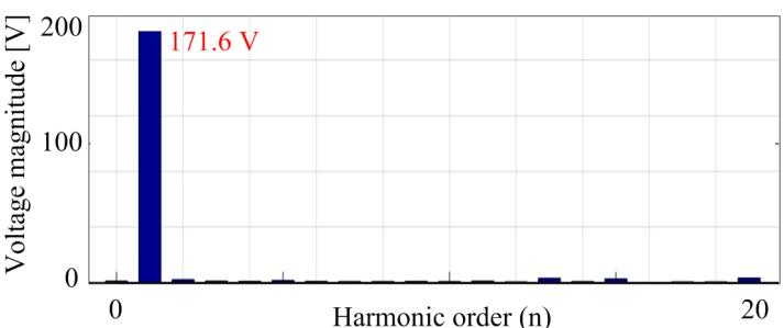
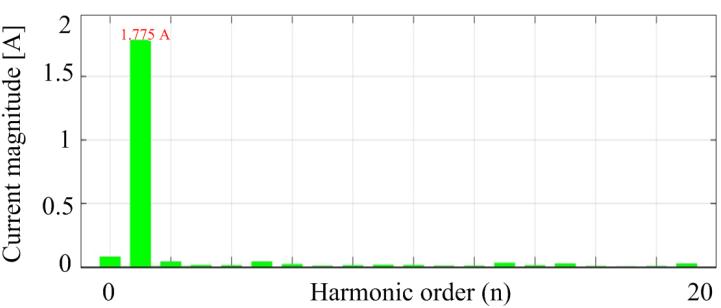
ThevoltagestressesovervariousswitchesareshowninFigure6a.WhentheR-LloadofR=50, L=80mHistaken into account, the FFT analysis of VRY yields the highest magnitude of the fundamental voltage of 171.6V with 31.08% of total harmonic distortion(THD),asshown inFig.6b. Similarto this,the FFTanalysisof iRY yields a fundamental current peakmagnitudeof1.775Awith1.45%THDasshowninFig.6c Itcapturessteady-statevaluesof100Vand96.5VoverCx1 andCx2,respectively.ItalsomentionsthatCx1 andCx2 havepeak-to-peakripplevaluesofabout2.5Vand2V,respectively.
Simulationsresultsforproposed3-ФSCMLItopology:(a)polevoltage,(b)linevoltages
(b)linevoltage,loadcurrentandvoltageacrosscapacitors


5. Comparison of Proposed SCMLI with existing 3-Ф MLI topologies
The primary goal of the presentedtopology is to produce the highestnumber of output voltage levels with the fewest possible power devicesand capacitors at the lowest possible cost The Component to Level Factor (FC/L) and the CostFunction(CF)aretwovariablesthatquantify themeritsofthesuggestedtopologyinthiscontext(CF).Theequation belowdefinesthecostfunctionandthefactorcomponenttolevelfactor(FC/L).

And,
Here,thenotationsrepresentnumberofpowerswitches= ,capacitors= ,auxiliarydiodes= NAD,sources= , numberofpolevoltagelevel= ,driverunits= ,polevoltagelevels= NL1,bodydiodes = NBD,andline-to-linevoltage levels= NL2.αistheweightfactorandnumberoftheinductors= NI.
Foracertainnumberofpolevoltagelevels,Table3includescomponentcount,costfunction,totalstandingvoltage, andvoltagegainthatcomparestheproposedtopologytotheexisting3-ФSCMLIstructures.MultipleisolatedDCsources arepresentinthetopologiesdescribedinRef.[14,15,20]toraisethevoltagelevel.Thetopologyinreference[12,14,15, 17,20]hasapoorabilitytoincrease.Despitehavingthepotentialtoraisevoltage,thetopologiesinref[9–11]areonly1.5 times as effective as the proposed one. Additionally, the proposed topology has a lower CF than recent topologies. The leastexpensivetopology,however,is[12,17].Itrequiresaboostingcircuit,whichaddsexpenseandcomplexity.
6. Conclusion
Athree-phaseSCinverterthatboostsvoltageeffectivelyisdescribedinthisarticle.Thesuggesteddesignisnotable for having the fewest active and passive switching components per level, lower cost function values, and self-balanced capacitor voltage. Due to these aspects, it is envisaged that the suggested topology will mostly be employed for solar panels,fuelcells,andelectriccars.Thepresentedmodulesynthesisessevenlevelsusingpowerswitchesthatareallrated at the same voltage as the input dc source. The proposed module is determined and analyzed and its MATLAB/Simulink simulation is described in this paper. A fair comparison of the newly presented SCMLI structure with other switched capacitors-based topologies further demonstrates its superior performance and competence in terms of semiconductor requirements.
7. References
[1] Abbott,D.:‘KeepingtheEnergyDebateClean:HowDoWeSupplytheWorld’sEnergyNeeds?’, Proc IEEE,2010,98,(1), pp.42-66
[2] RodriguezJ,LaiJS,PengFZ(2002) Multilevelinverters:asurveyoftopologies,control,andapplications.IEEETrans IndElectron49(4):724–738.
[3] GuptaKK,RanjanA,BhatnagarP,SahuLK,JainS(2016)Multilevelinvertertopologieswithreduceddevicecount:a review.IEEETransPowerElectron31(1):135–151.
[4] Gupta KK, Jain S (2012) Topology for multilevel inverters to attain the maximum number of levels from given DC sources.IETPowerElectron5(4):435–446.
[5] Babaei E, Gowgani SS (2014) Hybrid multilevel inverter using switched capacitor units. IEEE Trans Ind Electron 61(9):4614–4621.

[6] K. Jena, C. K. Panigrahi, K.K. Gupta, D Kumar, N. K. Dewangan (2022) Generalized Switched-Capacitor Multilevel InverterTopologywithSelf-BalancingCapacitors.JournalofPowerElectronics22(9):1617-1626.
[7] PonrajRP,SigamaniT,SubramanianVA(2021)DevelopedHbridgecascadedmultilevelinverterwithreducedswitch count.JElectrEngTechnol16:1445–1455.
[8] RamanSR,ChengKWE,YeY(2018)Multi-inputswitchedcapacitormultilevelinverterforhigh-frequencyACpower distribution.IEEETransPowerElectron33(7):5937–5948.
[9] Lee SS, Bak Y, Kim SM, Joseph A, Lee KB (2019) New family of boost switched-capacitor seven-level inverters (BSC7LI).IEEETransPowerElectron34(11):10471–10479.
[10] ZengJ,LinW,LiuJ(2019)Switched-capacitor-basedactiveneutral-point-clampedseven-levelinverterwithnatural balanceandboostability.IEEEAccess7:126889–126896.
[11] JagabarM, Sandeep N, Blaabjerg F (2019) High gain active neutral point clamped seven-level self-voltage balancing inverter.IEEETransCircuitsSystIIExpressBriefs67:1–1.
[12] Abhilash T, Annamalai K, Tirumala SV (2019) A seven-level VSI with a front-end cascaded three-level inverter and flyingcapacitorfedH-bridge.IEEETransIndAppl55(6):6073–6088.
[13] Roy T, Sadhu PK, Dasgupta A, Aarzoo N (2019) A novel three phase multilevel inverter structure using switched capacitorbasicunitforrenewableenergyconversionsystems.IntJPowerElectron10(1/2):133–154.
[14] SalemA,AhmedM,OrabiEM,AhmedM(2015)Newthree-phasesymmetricalmultilevelvoltagesourceinverter.IEEEJ EmergSelTopCircuitsSyst5(3):430–442.
[15] Raushan R, Mahato B, Jana KC (2016) Comprehensive analysis of a novel three-phase multilevel inverter with the minimumnumberofswitches.IETPowerElectron9(8):1600–1607.
[16] P.Bhatnagar,R.Agrawal,N.K.Dewanganetal.(2019)Nine-levelVoltage-DoublerBi-polarModuleforMultilevelDC toACPowerConversion," IET Power Electronics 12(15):4079-4087.
[17] Siwakoti YP, Mahajan A, Rogers DJ, Blaabjerg F (2019) A novel seven- level active neutral-point-clamped converter withreducedactiveswitchingdevicesandDC-linkvoltage.IEEETransPowerElectron34(11):10492–10508.
[18] LiuJ,WuJ,ZengJ,GuoH(2017)Anovelnine-levelinverteremployingonevoltagesourceandreducedcomponents ashigh-frequencyACpowersource.IEEETransPowerElectron32(4):2939
2947.
[19] P. Bhatnagar, R. Agrawal, N. K. Dewangan et al. (2019) Switched- Capacitors 9-level Module (SC9LM) with Reduced DeviceCountforMultilevelDCtoACPowerConversion.IETElectricPowerApplications13(10):1544-1552.
[20] Salem A, Ahmed EM, Orabi M, Abdelghani AB (2014) Novel three-phase multilevel voltage source inverter with reducedno.ofswitches.In:ProcIntRenewableEnergyCongr,pp.1–5.
[21] Lee SS, Lim CS, Lee KB (2020) Novel active-neutral-pointclamped inverters with improved voltage-boosting capability.IEEETransPowerElectron35(6):5978–5986.

[22] LeeSS,Siwakoti YP,BarzegarkhooR,Lee KB(2021)Switchedcapacitor- based5-level t-typeinverter(SC-5TI)with soft-chargingandenhancedDC-linkvoltageutilization.IEEETransPowerElectron.
[23] A Iqbal, MD Siddique, BP Reddy, I Khan (2021) A high gain 9L switched-capacitor boost inverter (9L-SCMI) with reducedcomponentcount.IEEETexaspowerandenergyconference(TPEC).
[24] Anwar A, Abbas MG, Khan I, Awan AB, Farooq U, Khan SS (2020) An impedance network-based three level quasi neutralpointclampedinverterwithhighvoltagegain.Energies13(5):1261.
[25] RichardeauF,PhamTTL (2013)Reliabilitycalculationofmultilevel converters:theoryandapplications.IEEETrans IndElectron60(10):4225–4233.
[26] Dwivedi A, PahariyaY(2021) Design and analysis of hybrid multilevel inverter for asymmetrical input voltages. J ElectrEngTechnol.
