SPEED CONTROL OF DC MOTOR USING DC/DC BOOST CONVERTER
 Satish D. Patel
Mishra
Dipkumar S. Trivedi
Joshi4
Satish D. Patel
Mishra
Dipkumar S. Trivedi
Joshi4
1Lecturer in Electrical Engineering, R C Technical Institute Sola Ahmedabad, Gujarat, India

2Lecturer in Electrical Engineering, K.D. Polytechnic, Patan, Gujarat, India
3Lecturer in Electrical Engineering, K.D. Polytechnic, Patan, Gujarat, India
4Lecturer in Electrical Engineering, K.D. Polytechnic, Patan, Gujarat, India ***
Abstract - This paper presents a design and simulation of DC/DC boost converter. This system has a nonlinear dynamic behavior, as it works in Dc-Dc Boost Converter switch-mode. When the changes on the load or on the line voltage at the input. The input usually is obtained by PV array and therefore the design and simulation in this paper covers the whole range of radiations and temperature. In this paper we analyze the equations of a boost converter and propose a design components and simulation of DC/DC boost converter. It is a high gain Transformer less Inverter modeling which is used for smart Grid Technology or as stand alone for home appliances is proposed. The proposed Tansformerless topology provides higher voltage gain, low cost, small size, and simple control. Stand alone Transformer less Inverter for home appliances.
Key Words: photovoltaic (PV), Boost Converter and matlabsimulation.
1. INTRODUCTION
Themassusageof thefossil fuels,suchastheoil,thecoal andthegas,resultinseriousgreenhouseeffectandpollute the atmosphere, which has great effect on the world. Meanwhile,thereisa bigcontradiction between the fossil fuelssupplyandtheglobalenergydemand,whichleadsto a high oil price in the international market recently. The energy shortage and the atmosphere pollution have been themajorlimitationsforthehumandevelopment.How to find renewable energy is becoming more and more exigent. The PV cell is density of power radiated from the sun at the outer atmosphere is 1.373 kW/m2. Final incident sun light on the earth surface has the peak density of 1 kW/m2 at noon in the tropics. Solar cell can converttheenergyofsunlightdirectlyintoelectricity[1].
1.1 EQUIVALENT CIRCUIT OF A PV CELL
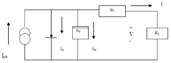
A simplified equivalent circuit of a solar cell consists of a currentsourceinparallel witha diodevariable resistor is connected to the solar cell generator as a load. Relationship between the current and voltage may be determinedfromthediodecharacteristicsequation:
I=Iph-Id = Iph-IO(eqv/kt-1)
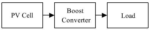
Whereqistheelectroncharge,kistheBoltzmann constant, ph I is the photocurrent, Io is the reverse saturation current, Id is the diode current and T is the solar cell operating temperature (K).[3] Switch mode DC to DC converters are used to match the output of a PV generatortoavariableload.DCtoDCconvertersallowthe charge current to be reduced continuously in such a way that the resulting battery voltage is maintained at a specifiedvalue.Apracticalphotovoltaicenergyconversion systemblockdiagramisshowninFig.2.
1.2 OVERVIEW OF A DC-DC CONVERTER
DC-DC converters can be used as switching mode regulators to convert an unregulated dc voltage to a regulated dc output voltage. The regulation is normally achieved by PWM at a fixed frequency and the switching device is generally BJT, MOSFET or IGBT. The minimum oscillator frequency should be about 100 times longer than the transistor switching time to maximize efficiency. This limitation is due to the switching loss in the transistor.Thetransistorswitchinglossincreaseswiththe switchingfrequencyandthereby,theefficiencydecreases. The core loss of the inductors limits the high frequency operation.ControlvoltageVcisobtainedbycomparingthe output voltage with its desired value. Then the output voltage can be compared with its desired value to obtain thecontrolvoltageVcr.ThePWMcontrolsignalforthedc converter is generated by comparing Vcr with a sawtooth voltageVr.[3].There are four topologiesfor the switching regulators: buck converter, boost converter, buck-boost
converter, cứk converter. Dc-Dc Boost Converter is a outputdcvoltageisgreaterthaninputdcvoltage
2. DC-DC BOOST CONVERTERS
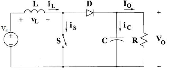
TheDC/DCconvertersarewidelyusedinregulatedswitch modeDCpowersupplies.Theinputoftheseconverters is an unregulated DC voltage, which is obtained by PV array and herefore it will be fluctuated due to changes in Radiation and temperature. In these converters the average DC output voltage must be controlled to be equatedtothedesiredvaluealthough theinputvoltage is changing. From the energy point of view, output voltage regulation in the DC/DC converter is achieved by constantly adjusting the amount of energy absorbed from the source and that injected into the load, the converter can herefore operate in two different modes depending uponitsenergystoragecapacityandtherelativelengthof the switching period. These two modes are known as discontinues conduction and continuous modes. The DC/DC boost converter only needs four external components: Inductor, Electronic switch, Diode and output capacitor. The converter can therefore operate in the two different modes depending on its energy storage capacity and the relative length of the switching period. The DC/DC converter has two modes, a Continuous Conduction Mode for high power conversion and Discontinuous Conduction Mode for low power or standbyoperation.
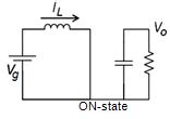
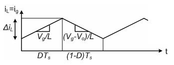
andterminatesatt=ton.TheinductorcurrentIL(t)greater thanzeroandrampuplinearly.TheinductorvoltageisVi. When the switch is ON, the inductor is charged from the input voltage source Vg and the capacitor discharges acrosstheload.
Dutycycle= ,whereT=1/f
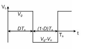
Inthefigure(3)showsastepuporPWMboostconverter. It consists of a dc input voltage source Vg; boost inductor L, controlled switch S, diode D, filter capacitor C, and the loadresistanceR.WhentheswitchSisintheonstate,the current in the boost inductor increases linearly and the diodeDisoffatthattime.WhentheswitchSisturnedoff, the energy stored in the inductor is released through the diodetotheoutputRCcircuit[4].
a) MODE1(0<t<ton)ONSTATE:
In the ON state, the circuit diagram is as shown below in Figure4,Mode1beginswhenIGBT'sisswitchedonatt=0
b) MODE2(ton<t<T)ONSTATE:
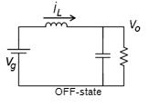
In the OFF state, the circuit becomes as shown in the Figure.
Mode 2 begins when IGBT's is switched off at t=ton and terminatesatt=Ts.Theequivalentcircuitforthemode2is shown in Fig. 5. The inductor current decrease until the IGBT's is turned on again during the next cycle. The voltageacrosstheinductorinthisperiodisVi-Vo.Sincein thesteadystatetimeintegralofinductorvoltageoverone timeperiodmustbezero. Whentheswitchisoff,thesum total of inductor voltage and input voltage appear as the loadvoltage.Showthewaveformonoutputvoltageacross theinductorandflowoftheinductorcurrent.
Fromthebalanceequitation,
Vg(Ton)+(Vo-Vg)(Toff)=0
Vg(DTs)+(Vo-Vg)(1-D)Ts=0
Vg(DTs)-Vg(DTs)-VgTs+VoDTs-VoTs=0
DividingbothsidesbyTs,
D Toff Ts Vg Vo 1 1
Where,
Vi:Theinputvoltage,V.
Vo:Theaverageoutputvoltage,V.
Ton:TheswitchingonoftheIGBT's,s
Toff:TheswitchingoffoftheIGBT's,s
Ts:Theswitchingperiod,s.
D:Thedutycycle. So,
Frominductorcurrentrippleanalysis,changeininductor current,
∆Il = Imax-Imin
∆Il = (Vg/L)*Ton
∆Il = (Vg/L)*D*Ts
∆Il = Vg*D/Fs*L
L = Vg*D/Fs*(∆Il)
Theboostconverteroperatesincontinuousconducting modeforL>Lbwhere,
Lb= Fs D D R 2* ) *(1 * 2
Thecriticalinductance,Lb,isdefinedastheInductance at theboundaryedgebetweencontinuousanddiscontinuous modes; the current supplied to the output RC circuit is discontinuous.Thusalargefiltercapacitorisusedtolimit theoutputvoltageripple.Thefiltercapacitormustprovide theoutputdccurrenttotheloadwhenthediodeDisoff.
Theminimumvalueofthefiltercapacitancethatresultsin thevoltagerippleVr[8]isgivenby,
Cmin = f R V Vo D * * *
3. DESIGN OF THE BOOST CONVERTER
Currentripplefactor(CRF):
Currentripplefactorshouldbeboundedwithin30%
Sothat, 1
1I I =30%
Voltageripplefactor(VRF):
Voltageripplefactorshouldbeboundedwithin5%, Sothatis, Vo Vo =5%
Switchingfrequency(fs):
InaboostConverterSwitchingfrequencyonaIGBTisa30 KHZApply.
GIVEN DATA:-
InputVoltage: 25Volt
OutputVoltage: 400Volt
LoadResistance: 400Ω
OutputCurrent: 1Amp.
(a) CALCULATIONOFDUTYCYCLE:-
ConversionratioM =
DutyCycleD=93.75%
(b) CALCULATIONOFARIPPLECURRENT:Il = 1Amp
Sothat 1
1I I = 30%
∆Il = 1*0.3Amp=0.3Amp.
(c) CALCULATIONOFARIPPLEVOLTAGE:Vo Vo =0.05%,∆Vo=0.05
(d) CALCULATIONONINDUCTORVALUE(L):
InductanceL = l I f D Vg * *
InductanceL =2.60mHenry.
(e) CALCULATIONOFACAPACITORVALUE:-
CapacitanceC=468uF.
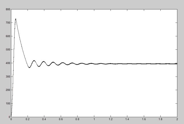
3. SIMULATION OF Open Loop DC –DC BOOST CONVERTER
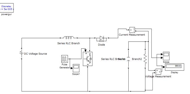
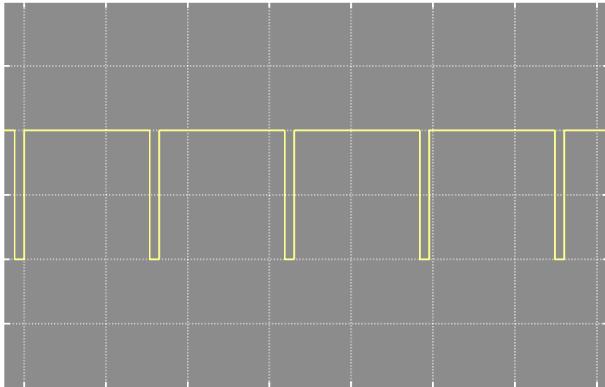
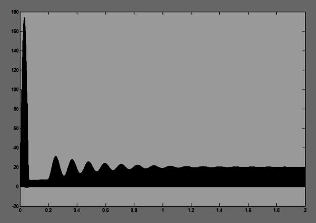
Using the MATLAB simulation program we get the result of Dc-Dc boost converter for 24V-400V DC Voltage. So designsectionvalueofinductorL=2.60Mh,Capacitorvalue C= 468uF and Resistor value R=300 ohm .show the waveform across the load voltage and inductance across the flow of current and gate pulse, and show observation variousdutycycleandacrosstheloadvoltage.
Variousdutycycleandoutputvoltageacrossload
Using the MATLAB simulation program get the result of Dc-Dc close loop boost converter for 24V-400V DC Voltage. So design section value of inductor L=2.60Mh,Capacitor value C= 468uF and Resistor value R=400 ohm .show the waveform across the load voltage and inductance across the flow of current and gate pulse, and show observation various duty cycle and across the loadvoltage.
3. CONCLUSIONS
This design of open loop and closed loop DC-DC Boost Converter provides smooth control of DC output for open loop and smooth output voltage for close loop DC-DC BoostConverter
REFERENCES
1. Md. Rabiul Islam, Youguang Guo, Jian Guo Zhu, M.G Rabbani, "Simulation of PV Array characteristics and Fabrication of Microcontroller Based MPPT", Faculty of Engineering and Information technology, University of Technology Sydney, Australia, 6th International Conference on Electrical and Computer Engineering ICECE 2010, 18-20 December 2010, Dhaka, Bangladesh.
2. SERBIAN JOURNAL OF ELECTRICAL ENGINEERING Vol. 7, No. 1, May 2010, 121-130 121 Simulation of Closed Loop Controlled Boost Converter for Solar Installation Athimulam Kalirasu1, Subharensu Sekar Dash2.
3. Muhammad H. Rashid, “Power Electronics circuits,DevicesandApplications”,ThirdEdition.
4. Modelling and Control design for DC-DC converter, PowerManagementgroup,AVLSILab,IIT-Kharagpur.
5. B.M Hasaneen, Faculty of Eng., Al-Azhar University, Kena, Egypt. And Adel A. Elbaset Mohammed Faculty of Engineering, Minia University, Minia, Egypt. “DESIGN AND SIMULATION OF DC/DC BOOST CONVERTER” From the SelectedWorks of Dr. Adel A. ElbasetDecember2008
6. Athimulam Kalirasu1, Subharensu Sekar Dash2 “Simulation of Closed Loop Controlled Boost Converter for Solar Installation” SERBIAN JOURNAL OF ELECTRICAL ENGINEERING Vol. 7, No. 1, May 2010,121-130