A LIGHT WEIGHT VLSI FRAME WORK FOR HIGHT CIPHER ON FPGA
Rajesh M S1
1Assistant Professor, Dept. of Electronics and Communication Engineering, College of Engineering Adoor, Kerala, India ***
Abstract - The field of communication has acquired various applications in the digital age. In recent years, the number of low-resource devices has grown significantly. Security and resource constraints are two issues that come up with such communication devices. Low resource systems are the focus of encryption methods known as lightweight cyphers, such as HIGHT cyphers. Flexible and rapid design of light-weight cyphers are used for reconfigurable platforms like fieldprogrammable gate arrays. The HIGHT cypher has easy operations and offers a sufficient level of protection. The implementation of a Hight cipher's lightweight VLSI design on an FPGA is presented in this study. It is appropriate for lowpower and low complexity applications. The size, power, and speed of the suggested VLSI design have been optimized. For faster throughput, the encryption and decryption procedures might be carried out simultaneously. Performance results for the suggested architecture's FPGA implementation are given. The outcomes demonstrate the effectiveness of the suggested architecture, with a throughput of 25 Mbps and an encryption and decryption delay of 0.64 ms Additionally the outcomes show that the suggested architecture is appropriate for lowpower applications.
Key Words: Lightweightcryptography,Blockciphers,VLSI architecture,FPGA,Lowresourcedevice.
1. INTRODUCTION
AstyleofcomputerarchitectureknownaslightweightVLSI focuses on combining lightweight and power-efficient componentstominimizethesystem'soverallsizeandpower consumption. This kind of architecture is becoming more andmorecommonasaresultofitscapacitytolowercosts and power usage while maintaining a high degree of performance[1].ApplicationsforlightweightVLSIdesigns include embedded systems, mobile phones, and medical equipment. They are also utilized in high-performance computing because they can deliver performance that is superiortothatofconventionaldesignswhilestillusingless electricity[2].Digitalsignalprocessor,fieldprogrammable gatearray(FPGA),application-specificintegratedcircuit,and system-on-chip designs are the core elements of a lightweightVLSIarchitecture.Thearchitectureiscreatedto make use of each of these components' strengths, such as FPGAs'lowpowerneedsandtheircapacitytohandleseveral jobsatonce[3].Powerefficiencyisthemostcrucialaspect toconsiderwhilecreatinga lightweightVLSIarchitecture. Thisrequirescarefulcomponentselectionandsystemdesign to ensure that overall power consumption is kept to a minimum. Applications based on intelligent low-resource
deviceshavebeensignificantlyexpandedrecently.Internet ofThings[4],radiofrequencyidentification[5],smartcards, wirelessbodyareanetworks,andwirelesssensornetworks areafewexamplesofsuchapplications.Numerousdesign factorsincludingarea,security,power,andenergymustbe takenintoaccounttogetthemaximumperformanceoutof theimplementedsystem.
For devices with less memory and processing capacity, conventionalencryptiontechniquesmightnotbesuitable. This prompted the creation of the "lightweight cryptography"branchofcryptologicreasoning.TheHIGHT algorithmswerecreatedexpresslytofittherequirementsof lightweightcryptology[6].
The "HIGHT" cypher, one of the well-known lightweight cyphers designed for low resource systems, must be highlighted before discussing the hardware FPGA implementation of lightweight cyphers. A hardwareoriented,lightweightblockcypheriscalledHIGHT[7].The HIGHTcipher'sstructureisamodificationofthegeneralized Feistel network [8] and makes use of simple hardwareoriented transform operations. Key length of HIGHT algorithmis128bitandblocksizeis64-bit.
Ingeneral,blockcypherscanbeimplementedinhardware or software. Compared to software designs, hardware implementations are faster and use less energy. Fieldprogrammablegatearray(FPGA)designsareoneapproach forimplementinghardwaredesigns.ThebenefitsofanFPGA designareflexibilityandashortdevelopmenttimeatalow cost [9]. Additionally, the FPGA's reconfigurability feature makesitadesirablechoiceforimplementingcryptographic algorithms. Reconfigurability makes it easier to modify, upgrade,andswapcypheralgorithmswhilestillinuse[10].
The designhas beenoptimizedtouse theleastamount of hardware resources and consume less power and energy. Althoughotherperformanceindicators,suchasspeed,are equallycrucial,powerandenergyarethemainproblemsfor low-resource systems. The HIGHT encryption was chosen becauseithasgoodenergyandthroughputperformanceand isdesignedforlow-resourceimplementation[11].
2. LITERATURE REVIEW
Thetopicofthearticle[13]isthedesignofspecialized VLSI intended for use in high-performance computing systems. General-purpose processor (CPU) and graphics accelerator(GPU) operate in the mode of general-purpose computingacceleration.Forthedesignofenergyadjustable

circuitsforopen-mindedapplication,approximatecomputing isgainingstrength.Alowpowerdiminishingregionsquare root(SQR)circuitisdescribedin[14]andachievesincredible region and energy efficiency while exhibiting insignificant errors in the results. For the purpose of reestablishing cluster-based square-pull circuits for challenging applications,twoapproximatedapproachesareputout.By usingtheBooleanarticulations,approximatedreestablishing subtractorcellsareusedinthemainconfigurationtoreplace specificSQRsubtractorcells.
[15] Presents an equipment-improved predicted adder with essentially no typical error and a typical error distribution, or Gaussian error. The suggested adder is referredtobytheauthorsasHOAANED,anditisexpandedas equipment updated rough adder with typical error dispersion.Forafairanalysis,authorstookintoaccountthe useofHOAANEDforcomputerizedpicturehandlingwiththe exact adder. In particular, the augmentations used precise and inexact adders separately to carry out rapid Fourier ChangeandretrogradequickFourierChangeoperationsto replicate the images. [16] Focuses on designing a Parameterizable SHA-256 algorithm implementation in an FPGA to teach blockchain concepts. The fundamental idea behindBlockchaindesignthataddssecurityandanonymity toasystemisSHA-256.Thisone-wayhashfunctioncreatesa singularresultforagiveninput,guaranteeingthevalidityand nonrepudiation of the data. The decentralization of blockchaintechnologyiscausingittobecomemoreandmore popularonline.
[17] Presents a 65-nm CMOS stage-locked circle with established sub stage-locked circle structure 32-GHz frequency-tweakedpersistentwavemodulator.Withthesub stage-lockedcircle,thelow-passinfluenceinstagespaceis acknowledged, lowering the impact of the delta sigma modulator'squantizationdisturbanceandspikes.Thestage spacemodelandstageclamourmodelarebrokendownand imitated in order to achieve excellent solidity and stage commotion execution. These models are discussed and reproduced in light of the trill linearity, which aids in determining the plan boundaries and verifies the linearity improvement. In [18], a precisely stage-controlled transmitteroperatinginthe76to81GHzbandisintroduced fortheautoradarapplication.Themulti-channeltransmitter usingthis finder achievesa progressive work error ofless than0.6°root-mean-squareinthe76to81GHzfrequency band. The fundamental functional unitto execute modular arithmeticinthedifferentcryptographyandpseudorandom bitgenerator(PRBG)methodsprovidedin[19]isthethreeoperandbinaryadder.Themethodthatismostfrequently used to execute three-operand addition is called the carry save adder. The suggested design is synthesized using a 32nm CMOS technology library that is commercially accessible,anditisalsoimplementedonanFPGAdevicefor functionalvalidation.For32-,64-,and128-bitarchitectures, respectively,thepost-synthesisresultsoftheproposedadder reported3.12,5.31,and9.28timesfasterthantheCS3A.
[20]introduceddifferentialpostponecomponent(DCDE) canachieveastageshiftof20psandanormalgoalof1.25ps thankstothetwoinformationbitsthatcontrolitsinclination currentandresistiveburdenandthetwootherpiecesthat organizeitsresultcapacitiveburdeninsidethedifferential current-mode rationale (CML) DCDE. Using a low-power block-sharing without offset recurrence following circle (FTL)[21]showshowtoalignthecyclevoltage-temperature varieties of the voltage-controlled oscillator (VCO) recurrence).
ManyapplicationsbuiltusingVLSIarchitecturehavebig sizecomponentsthatcauseadesignfaultinthefilterduring floating point arithmetic stages. To increases design complexity and the time delay effect the architectural paradigm must be changed. The rising number of components,especiallydelayelements,isaprobleminVLSI architectures for finite impulse response (FIR) filters [22]. Thisarticleoffersacross-foldedshiftingimplementationof the floating point processing element for the VLSI architecturethathasbeenalteredtouselessregisters.The suggestedFIRfiltersystemenhancesthecomplexityandhigh delayrateofthelogicaloperationbyreducingthenumberof componentsinthecircuit.
Forone-layered(1-D)wavelet-basedelectrocardiography (ECG)pressureframeworkswithqualityassurance,aspeed andpower-effectivesetapportioninginvariousleveledtrees (SPIHT)planisofferedin[23].Toovercomethechallengesof lowcodingspeedandcomplexequipmentdesigntheauthors firstproposeacoding-timeandcalculationeffectiveSPIHT calculation using various types of coding status register record.EarlierSPIHTcalculationsarethendescribedbythe authorsfordynamiccalculationandcourseofactioninthe arranging and refinement handling stage that were necessary.You-only-look-once(YOLO)CNNisimplemented in a Tera-OPS streaming hardware accelerator by [24] for real-time object identification with great throughput and powerefficiency.FPGAcanstorethewholenetworkmodelin its block RAMs thanks to the binary weight, which significantly reduces off-chip accesses and boosts performance. For better hardware consumption, the suggestedapproachfullypipelineseachconvolutionallayer. ThebestpowerefficiencyisachievedbythisCNNthatuses theVC707FPGAandcanhandle1.877teraoperationsper second(TOPS)at200MHzwithbatchprocessingwhileonly requiring18.29Wofon-chippower.
[25]Makesaproposalforaclosedstructurearticulation for determiningthebase operatingvoltage(VDDmin)ofD flip-flops(FFs).Thebaseinventoryvoltageatwhichtheflip flopsarefunctionalwithouterrorsisreferredtoasVDDmin. ThesuggestedexplanationillustratesthatVDDminofFFsisa direct function of the square root of the logarithm of the numberofflipflops,andthatbothitsinclinationandcatch dependonthecompatibility.Thereconstructionresultsas wellasthesiliconestimationssupporttheplannedVDDmin articulation.Finally,theauthorsdiscussVDDmin'sreliance ondeviceboundaries.Hybridfloatingpoint(FP)executions
in[26]advanceprogrammingFPexecutionwithoutcreating a space overhead from FP units with all of the necessary equipment.Thesuggestedexecutionsarebuiltintotinyfixedpoint processor witha RISC-like architectureusing 65-nm CMOStechnology.
A technique in [27] allows for the effective use of field programmable gate array hardware resources while computing all of the CNN's layers. Compared to the basic GEMM-baseddesign,itexhibitsperformanceimprovements in the range of 1.4 to 4.02 with only 13% more FPGA resources. Popular CNN models like AlexNet and VGG-16 have been mapped onto the suggested accelerator by the authors,andthemeasuredperformancecomparesfavorably to other recent implementations [28]. The CNN is implemented using the VC707 FPGA, which has the best power efficiency, achieving a throughput of 1.877 tera operations per second. The CPU first divides large circuits intoseveralsegments,whicharethentransmittedonebyone totheFPGAforrandomwalking[29].Bydirectingindividual part of the algorithms to the appropriate architecture and building the FPGA bit stream just once, the framework overcomestheproblemoflimitedfieldprogrammablegate arrayon-chipresourcesandintegratesbothbenefitsofFPGA and CPUs. In order to increase the performance of FPGAs, various kernel optimization techniques are employed. In order to obtain the findings in [30], a hamming error detection and correction code has been constructed in Verilogger pro 6.5 after an algorithm for encoding and decodinghammingcodeshasbeenexplained.Hammingcode, whichisimplementedinVerilog,isanupgradedformofthe paritycheckmethodthattransmitsn-bitsofinformationdata with redundancy bits. The design procedure for hamming codeutilizingVLSIisattemptedtobeexplainedinthiswork becauseFPGA isa morecost-effectivetechnologythan the alternatives.
[31] Offer FPGA implementation of the AES algorithm based on high-level synthesis. The implementation, which makes use key of a 128-bit length, is ideal for telecom applicationslike5G.Thisisduetotheirreconfigurableand parallelarchitectures.Becauseoftheirquickerspeeds,FPGAs arealsousedasplatformforsoftwaredevelopmentinpresilicon environment. High-Level Synthesis (HLS) tools are alsoheavilyutilizedbythedesigncommunityinVLSIdesign flows.
Because of their small region, modest power, wide tuning range, and ease of scaling with process innovation, ring oscillators (ROs) are well recognized. However due to ineffectivestageclamourandjitteryexecution,itsusagein many applications is constrained. Warm loudness and glitteringturbulencecausesjitter,which,incontrast,lessens with fluctuating repetition. [32] Depicts a method for reducingjitterinROscalledrecurrenceassistance.Authors supporttheinteriorswayingrecurrenceinordertomaintain theidealresultrecurrence,andpresentarecurrencedivider aftertheoscillator.Thistechniqueoffersreducedjitteralong
with the opportunity to trade off yield jitter for power for dynamicexecutionoftheboard.
3. METHODOLOGY
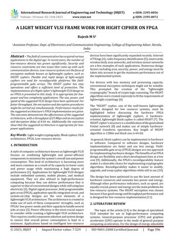
A block cypher called HIGHT is appropriate for low-cost, low-power, and ultra-lightweight applications. The major featuresofHIGHTincludeblocklengthof64-bit,keylength of 128-bit, 8-bit oriented operations, and a 32-round iterative structure. As a result, the encryption and decryption processes are identical, but the sequence in whichtheblocksareappliedisreversed.
HIGHT's encryption step includes a preliminary transformation,followedby transformationsof32rounds and a final transformation. The simple operation mod 28 addition, bitwise rotations, and exclusive-or make up the majority of each of the 32 rounds. The main scheduling is divided into two parts: Generations of "whitening keys" (WKs)and"subkeys"(SKs).FourWKsareutilizedineachof the initial and final transformations, which both use the WKs.Thepseudo-randomgeneratedconstantsandmod28 additionoftheMKareutilizedtocreatetheSKthatareused inthe32roundoftransformation.FourSKsareutilizedin eachofthe32rounds,totaling128SKs,whicharecreated. WKsandSKsarethetwokey-generationalgorithmsusedin the key schedule. Mapped to WK0, WK1, WK2, and WK3, respectively, are MK12, MK13, MK14, and MK15. The correspondingWK4, WK5, WK6, and WK7codesforMK0, MK1, MK2, and MK3 are listed below. To maximize the hardwareresource,includingarea,power,andenergyofthe
fundamentaldesign,theFPGAimplementationsusingmany roundsareaddressedandinvestigated.Theproductionoftermsandtheexecutionofthenumberofroundsarethetwo mainpartsofthedesignoptimizationthatareinvestigated. Oneoftheprimarydesignissuesfortheformerisgenerating terms, thus welooked at two implementation techniques: thelinearfeedbackshiftregister(LFSR)method[34]andthe lookup-table(LUT)method.Forthelatter,bothsingle-round and multiple-round implementations of the number of roundsinthehardwareareexplored.
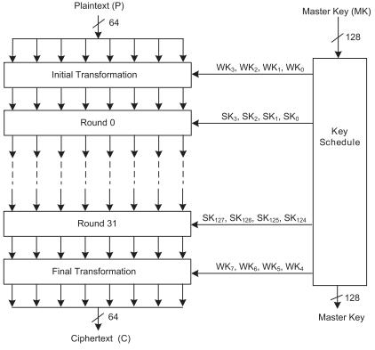
usingwiththeXilinxVirtex-5xc5vlx110t-1ff1136servingas the target FPGA device. Table I includes the FPGA Device Utilization Summary as well as a number of other performancemetrics.Resultsfromsimulation,synthesis,are presented.TheAreaReductiondesigntechniquewasusedto achievethebenchmarkresultsshowninTABLEI,withthe speedsetto-1andallothersettingsarekept.TABLEImakes it very clear that the suggested architecture only employs 0.45percentoftheavailableSlice,ofwhich0.36percentare Slice Register and 0.40 percent are Slice LUTs. When evaluatedinvariousscenarios,thesuggesteddesignexhibits evengreaterqualities.Whenthespeedsettingissetto -2, the maximum frequency soars to 459 MHz, indirectly enhancing the throughput. Numerous additional metrics have been noticed. The reporting of results has, however, adoptedaconsistentmethodology.
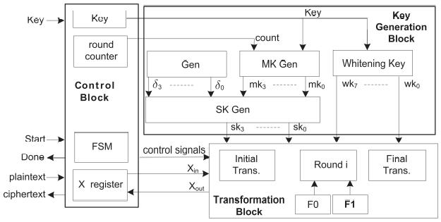
2:FPGADesignHIGHT
3.1 One round design forbasic Field Programmable Gate Array
The architecture of the HIGHT Field programmable gate arrayimplementationisdepicts infigure2forone round, which is consist of control logic, key generation, and transformation.Theinteractionwiththeexternalsystemand executes the algorithm's activity sequencing capability managedbythecontrolblock.Thecontrollogicisinstructed tostarttheencryptionprocessbythestartinputsignal,and theencryptionisfinishedbythedoneoutputsignal.Thekey, round,andX-registerarethethreeregistersarecontrolled by the control logic. 32 rounds involved in the round counter. The key generation block generates the WK and ensuingSK.TheMKbytesareprimarilyusedtoconstructthe WK,andthetermsandMKbytesarecombinedtocreatethe SKs. The initial transformation, followed by the 32 round transformations,andthefinaltransformationareallputinto actionbythetransformationblock.According totheLFSR implementationapproach,eachroundshouldresultinthe production of four unique words. Therefore, each transformationroundhasfourLFSRblocks.TheusageofFF is often large and power consuming, is the fundamental drawbackoftheLFSRarchitecture.
3.2 Experimental Result
The suggested architecture has been successfully synthesizedandimplementedinXilinxISEDesignSuite14.7
4. CONCLUSIONS
OnanFPGA,aLightweightVLSIArchitecturefortheHIGHT Cipher was successfully implemented. The HIGHT cypher encryptionanddecryptionfunctionalitywasbuiltintothe architecture.Theencryptionanddecryptionthroughputof theFPGAimplementationwas25Mbpswith0.64mslatency. Both the area and the performance both exhibit improvement.Akeysizeof128bitsisalsosupportedbythe FPGAimplementation,offeringahighlevelofsecurity.The suggesteddesignoffersagoodthroughputorareatrade-off
incomparedtothecurrentserialandparallelsystems.The conceptoffersaquick,cost-efficient,andsecurealternative forsecurecommunication.Forembeddedsystemsthatneed good security and minimal power consumption, the suggestedarchitectureisasuitablesolution.
REFERENCES
[1] Yarlagadda,S.,Kaza,S.,chowdaryTummala,A.,Babu,E. V.,&Prabhakar,R.(2021).ThereductionofCrosstalkin VLSI due to parallel bus structure using Data CompressionBusEncodingtechniqueimplementedon Artix7FPGAArchitecture.InformationTechnologyIn Industry,9(1),456-460.
[2] Somashekhar, V. M., & Singh, R. P. (2020). FPGA implementationoffaulttolerantadderusingverilogfor highspeedVLSIarchitectures.InternationalJournalof Engineering and Advanced Technology (IJEAT) ISSN, 2249-8958.
[3] Palchaudhuri, A., & Dhar, A. S. (2021). Speed-area optimized VLSI architecture of multi-bit cellular automaton cell based random number generator on FPGAwithtestablelogicsupport.JournalofParalleland DistributedComputing,151,13-23.
[4] Atzori,L.,Iera,A.,&Morabito,G.(2010).Theinternetof things: A survey. Computer networks, 54(15), 27872805.
[5] Rolfes,C.,Poschmann,A.,Leander,G.,&Paar,C.(2008). Ultra-lightweight implementations for smart devices–security for 1000 gate equivalents. In Smart Card Research and Advanced Applications: 8th IFIP WG 8.8/11.2 International Conference, CARDIS 2008, London,UK,September8-11,2008.Proceedings8(pp. 89-103).
[6] HongD,SungJ,HongS,LimJ,LeeS,KooBS,LeeC,Chang D, Lee J, Jeong K, Kim H. HIGHT: a new block cipher suitable for low-resource device. In Cryptographic HardwareandEmbeddedSystems-CHES2006.Springer, 2006;46–59.
[7] Knudsen, L. R. (2005, June). Practically secure Feistel ciphers. In Fast Software Encryption: Cambridge Security Workshop Cambridge, UK, December 9–11, 1993Proceedings(pp.211-221).
[8] Wollinger,T.,Guajardo,J.,&Paar,C.(2004).Securityon FPGAs: State-of-the-art implementations and attacks. ACM Transactions on Embedded Computing Systems (TECS),3(3),534-574.
[9] Uthayakumar,C.,Jijina,G.O.,Suresh,G.,&Nagaraju,V. (2021, July). FPGA Based Approximate Digital VLSI CircuitValidatingFocusedonFaultDiagnosis.InJournal of Physics: Conference Series (Vol. 1964, No. 6, p. 062079).
[10] Sowmya, N., & Rout, S. S. (2021). A Review on VLSI Implementation in Biomedical Application. In Innovations in Bio-Inspired Computing and Applications: Proceedings of the 10th International ConferenceonInnovationsinBio-InspiredComputing andApplications(IBICA2019)heldinGunupur,Odisha, IndiaduringDecember16-18,201910(pp.130-138).
[11] Lian,X.,Liu,Z.,Song,Z.,Dai,J.,Zhou,W.,&Ji,X.(2019). High-performance FPGA-based CNN accelerator with block-floating-point arithmetic. IEEE Transactions on Very Large Scale Integration (VLSI) Systems, 27(8), 1874-1885.
[12] Kim,S.,Na,S., Kong,B.Y.,Choi,J.,& Park,I.C.(2021). Real-time SSDLite object detection on FPGA. IEEE Transactions on Very Large Scale Integration (VLSI) Systems,29(6),1192-1205.
[13] Tarasov, I. E. (2019, October). Architectures of highperformance VLSI for custom computing systems. In JournalofPhysics:ConferenceSeries(Vol.1333,No.2,p. 022019)
[14] Arya,N.,Soni,T.,Pattanaik,M.,&Sharma,G.K.(2020, January).Areaandenergyefficientapproximatesquare rooters for error resilient applications. In 2020 33rd internationalconferenceonVLSIdesignand202019th internationalconferenceonembeddedsystems(VLSID) (pp.90-95).IEEE.
[15] Nayar,R.,Balasubramanian,P.,&Maskell,D.L.(2020, July). Hardware optimized approximate adder with normal error distribution. In 2020 IEEE Computer SocietyAnnualSymposiumonVLSI(ISVLSI)(pp.84-89). IEEE.
[16] Devika, K. N., & Bhakthavatchalu, R. (2019, April). Parameterizable FPGA implementation of SHA-256 using blockchain concept. In 2019 International Conference on Communication and Signal Processing (ICCSP)(pp.0370-0374).IEEE.
[17] Fu,Y.,Li,L.,Liao,Y.,Wang,X.,Shi,Y.,&Wang,D.(2020). A 32-GHz nested-PLL-based FMCW modulator with 2.16-GHz bandwidth in a 65-nm CMOS process. IEEE Transactions on Very Large Scale Integration (VLSI) Systems,28(7),1600-1609.
[18] Fujibayashi,T.,&Takeda,Y.(2019).A76-GHzto81-GHz, 0.6 RMS phase error multichannel transmitter with a novelphasedetectorandcompensationtechnique.IEEE Solid-StateCircuitsLetters,2(12),277-280.
[19] Panda,A.K.,Palisetty,R.,&Ray,K.C.(2020).High-speed area-efficientVLSIarchitectureofthree-operandbinary adder. IEEE Transactions on Circuits and Systems I: RegularPapers,67(11),3944-3953.
[20] Rehman, S. U., Khafaji, M. M., Carta, C., & Ellinger, F. (2019).A10-Gb/s20-psdelay-rangedigitallycontrolled differential delay element in 45-nm SOI CMOS. IEEE Transactions on Very Large Scale Integration (VLSI) Systems,27(5),1233-1237.
[21] Yang, S., Yin, J., Mak, P. I., & Martins, R. P. (2018). A 0.0056-mm 2− 249-dB-FoM all-digital MDLL using a block-sharing offset-free frequency-tracking loop and dualmultiplexed-ringVCOs.IEEEJournalofSolid-State Circuits,54(1),88-98.
[22] John, T. M., & Chacko, S. (2021). FPGA‐based implementationoffloatingpointprocessingelementfor the design of efficient FIR filters. IET Computers & DigitalTechniques,15(4),296-301.
[23] Hsieh,J.H.,Hung,K.C.,Lin,Y.L.,&Shih,M.J.(2017).A speed-and power-efficient SPIHT design for wearable quality-on-demand ECG applications. IEEE Journal of BiomedicalandHealthInformatics,22(5),1456-1465.
[24] Nguyen,D.T.,Nguyen,T.N.,Kim,H.,&Lee,H.J.(2019). A high-throughput and power-efficient FPGA implementationofYOLOCNNforobjectdetection.IEEE Transactions on Very Large Scale Integration (VLSI) Systems,27(8),1861-1873.
[25] Fuketa, H., & Matsukawa, T. (2017). A closed-form expressionforminimumoperatingvoltageofCMOSD flip-flop. IEEE Transactions on Very Large Scale Integration(VLSI)Systems,25(7),2007-2016.
[26] Pimentel, J. J., Bohnenstiehl, B., & Baas, B. M. (2016). Hybrid hardware/software floating-point implementations for optimized area and throughput tradeoffs. IEEE Transactions on Very Large Scale Integration(VLSI)Systems,25(1),100-113.
[27] Kala,S.,Jose,B.R.,Mathew,J.,&Nalesh,S.(2019).Highperformance CNN accelerator on FPGA using unified winograd-GEMM architecture. IEEE Transactions on Very Large Scale Integration (VLSI) Systems, 27(12), 2816-2828
[28] Sikka, P., Asati, A., & Shekhar, C. (2020, November). Area-optimal FPGA implementation of the YOLO v2 algorithmusingHigh-LevelSynthesis.In2020IEEE7th Uttar Pradesh Section International Conference on Electrical, Electronics and Computer Engineering (UPCON)(pp.1-6).IEEE.
[29] Wei, X., Yan, C., Zhou, H., Zhou, D., & Zeng, X. (2019, March).AnefficientFPGA-basedfloatingrandomwalk solverforcapacitanceextractionusingSDAccel.In2019 Design, Automation & Test in Europe Conference & Exhibition(DATE)(pp.1040-1045).IEEE.
[30] ShahariarParvez,A.H.M.,MizanurRahman,M.,Podder, P., Hossain, M., & Islam, M. A. (2019). Design and
implementationofhammingencoderanddecoderover FPGA. In International Conference on Computer Networks and Communication Technologies: ICCNCT 2018(pp.1005-1022).
[31] Sikka,P.,Asati,A.R.,&Shekhar,C.(2020).Speedoptimal FPGAimplementationoftheencryptionalgorithmsfor telecom applications. Microprocessors and Microsystems,79,103324.
[32] Lee,T.H.,&Abshire,P.A.(2016).Frequency-boostjitter reduction for voltage-controlled ring oscillators. IEEE Transactions on Very Large Scale Integration (VLSI) Systems,24(10),3156-3168.
[33] Lim, Y. I., Lee, J. H., You, Y., & Cho, K. R. (2009). Implementation of HIGHT crypticcircuitforRFIDtag. IEICEElectronicsExpress,6(4),180-186.
[34] Weste,N.H.,&Harris,D.(2015).CMOSVLSIdesign:a circuits and systems perspective. Pearson Education India.