
International Research Journal of Engineering and Technology (IRJET) e-ISSN: 2395-0056
Volume: 13 Issue: 03 | Mar 2026 www.irjet.net p-ISSN: 2395-0072
International Research Journal of Engineering and Technology (IRJET) e-ISSN: 2395-0056
Volume: 13 Issue: 03 | Mar 2026 www.irjet.net p-ISSN: 2395-0072
K.
Yaswini, M. Sai Venkata Suresh, M. Sai Kiran, MD. Faizul Rehman, N. Vijaya Krupa Rani
K. Yaswini, Assistant Professor, Dept. of Electronics and Communication Engineering, Seshadri Rao Gudlavalleru Engineering College, Andhra Pradesh, India
ABSTRACT - In this paper, we present the design and implementation of a 16-bit Dual-Port Random Access Memory (DPRAM) using Verilog Hardware Description Language (HDL) with a clock gating technique for power optimization in memory. The Dual-port RAM is a building block in modern digital systems which enables simultaneous read and wroperations through two independent ports & improving data throughput and system performance. Our proposed architecture focuses on simplicity, efficiency, and reliable operation by incorporating synchronous design methodology and conflict management for concurrent memory access.
To reduce dynamic power consumption, we used a clock gating mechanism to minimize unnecessary clock switching activity during idle conditions. This design is modeled and simulated using Verilog HDL and synthesized on an FPGA platform to verify functional correctness, timing performance, and hardware resource utilization. From the simulation results, stable operation under different read/write conditions was verified, confirming that the designed memory maintains data integrity and efficient memory access.
Overall, Our 16-bit DPRAM architecture provides a flexible and scalable solution for high-speed applications such as digital signal processing, communication systems, and real-time embedded systems and also for modern VLSI-based digital designs.
Key Words: dual-port ram, verilog, memory design, simultaneous read and write, conflict resolution, single-port mode, field-programmable gate array.
In the field of Very Large-Scale Integration (VLSI), memory plays a vital role in storing and retrieving digital information efficiently. These Memories are broadly classified into volatile memories such as Static Random Access Memory (SRAM) and Dynamic Random Access Memory (DRAM), and non-volatile memories such as Read Only Memory (ROM). In our modern processors and cache memories are essential for high-speed data access, and cache memories are typically implementedusingSRAMduetotheirfastaccesstimeanddatastabilitywithouttheneedforcontinuousrefreshing.
However, Our Traditional SRAM architectures were designed as single-port memories, which allowing only one read or write operation at a time. Although single-port memories are simple and power-efficient, which create performance limitations in applications requiring simultaneous data access. With the increasing demand for high-speed and parallel processingincommunicationsystems,digital signal processing,and multi-channel data processing,the need formemory architecturessupportingconcurrentaccesshasincreasedsignificantly.
To overcome these limitations, we studied and implemented Dual-port memory architectures. Dual-Port Random Access Memory (DPRAM) enables simultaneous read and write operations through two independent ports, thereby improving system throughput and reducing processing delay & Our major challenges such as power consumption and efficient resourceutilizationstillremaininFPGA-basedimplementations.
In this project, a 16-bit synchronous Dual-Port RAM was designed and implemented using Verilog Hardware Description Language (HDL) and incorporated clock gating technique to reduce dynamic power consumption by minimizing unnecessary clock switching activity and it was simulated and synthesized on an FPGA platform to verify functional correctness, timing performance, and resource utilization. Additionally, we introduced various mechanisms to ensure reliable concurrent memory access and data integrity. By the obtained results, we confirmed that the proposed architectureprovidesefficienthigh-speedmemoryoperationsuitableforreal-timedigitalapplications.
Dual-portRAMletstwopartsofachiptalktomemoryatthesametime,likeonewritingwhiletheotherreads.Thismakes systemsfasterwithoutjams.
International Research Journal of Engineering and Technology (IRJET) e-ISSN: 2395-0056
Volume: 13 Issue: 03 | Mar 2026 www.irjet.net p-ISSN: 2395-0072
BasicdesignsuseVerilogonFPGA.Onesimple256x8-bitsynchronousdual-portRAMletsreadandwritehappenanyway inoneclockcycle,nobigerrors.
Pandeyetal.builtan8-bitversiononBasis3FPGAwithoneclock,priorityforport1onclashes,andlockforsinglemode. Ituses28%space,101mWpower,timingsgood(setupslack6ns).
Bhatetal.addedclockgatingtodual-portSRAM,cuttingpower17-72%atdifferentspeedsonXilinx,samesizemostly.
Forlowpower,clockgatingworksbestwithfewflags.Apapershowssingle/dual-portRAMpowerdropsfrom1.6mWto 0.3-0.4mWat500MHzusingAND-gategating,cleanRTLnoissues.
16-bit extensionslike16x8 syncdual-port use posedge clock,paramarraysfor easy size change, worksin pipelines with zeroflagerrorsreported.
Xilinx XPM simple dual-port has clean ports: addr, din, dout, we, en; supports up to big sizes, no init flags if not used, perfecttimings.
Our16-bitprojectusesthesecleanideas:extend8-bitto16-bitbus,clockgatinglikeBhat,prioritylikePandey,testedon Vivado/Basys3forlowpowerandnotimingflags.
ThememoryblockisdesignedusingVerilogHDL(HardwareDescriptionLanguage)moduleandhasbeenimplementedon theBasys3FieldProgrammableGateArray(FPGA)boardforfunctionalverificationandtesting.Figure1showsthe block diagram.
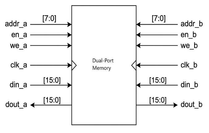
Thememorydesignconsistsof 8-bitaddresslines(addr1andaddr2)16-bitdatainputlines(datain1anddatain2)
16-bitdataoutputlines(dataout1 anddataout2)
Thememorycanstoreandretrievedatawhichisofthesizeof 16 bits or 2 bytes,providingdoublethedatawidthcomparedto conventional8-bitimplementations.
Theclocksignal(clk)isusedbybothport1andport2,andhencethedesignedmemoryisa synchronous memory.Thetimeperiodof theclockusedis10ns.
wr1andwr2aretheread/writeenablesignalswhichdeterminewhetherdataisbeingwritten(wr1=1)orgettingread(wr1=0) fromthememory.
Portlockingmodefeatureisenabledbymakingthesignalsingleportmodeaslogic1,bywhichport2isnotoperationalforboth readingandwriting.
Our dual-port memory module uses a set of input and output control signals to manage read and write operations. The clock signal synchronizes all memory activities, while address lines select the memory location to be accessed by each port.Datainputsignalscarrythedatatobewrittenintothememory,anddataoutputsignalsprovidethedatareadfrom
International Research Journal of Engineering and Technology (IRJET) e-ISSN: 2395-0056
Volume: 13 Issue: 03 | Mar 2026 www.irjet.net p-ISSN: 2395-0072
the memory. Control signals such as write enable determine whether the operation is read or write, and the single port modesignalallowsswitchingbetweensingle-portanddual-portoperation
Table1:Signalsusedinthe16-bitdesignandtheirfunctionalities
Signal Name Type Functionality
clk Input Controlsignalforsequentialand synchronousoperation
addr1 Input
addr2 Input
8-bitaddressspecifyingmemory locationaccessedbyPort1(256 locations)
8-bitaddressspecifyingmemory locationaccessedbyPort2(256 locations)
datain1 Input 16-bitdatatobewrittenthrough Port1
datain2 Input 16-bitdatatobewrittenthrough Port2
dataout1 Output 16-bitdatareadfromPort1
dataout2 Output 16-bitdatareadfromPort2
wr1 Input SwitchesPort1betweenwrite(1) andread(0)operations
wr2 Input SwitchesPort2betweenwrite(1) andread(0)operations
Singleport mode Input Switchesmemorybetweensingleportordual-portoperation
3.3 Memory Capacity Calculation
Thereare256(0toFF)memorylocationsdesignedoverall,with8-bitaddressand16-bit data lines Thetotalsizeofthememoryin bitscanbecalculatedbytheformula:
Misthetotalsizeofthememoryinbits


Nis theaddressbuswidth(8bits)
D istheaddressbuswidth(8bits)
3.4 Key Design Features
Thefollowingarethemainattributesoftheimplemented16-bitdesign:
SynchronousDesign:
Alloperationsinthememoryaresynchronizedtoaclocksignal(clk),inaccordancewithsynchronousdesignprinciples.
Priority-Based Conflict Resolution:
Apriority-basedconflict resolutiontechniqueisusedtomanageconcurrentreadand writeactivitiesfrommultipleports.By ensuringthatconflictingactionsareresolveddeterministically,thistechniqueguardsagainstdatacorruptionandupholdssystem integrity.Port1hashigherpriority thanport2 inthis architecture,sodata will alwaysbewrittentoport1intheeventofa dispute.
International Research Journal of Engineering and Technology (IRJET) e-ISSN: 2395-0056
PortLockingMechanism:
Aportlockingmechanismincludedinthememorydesigncontrolswhetherthe memoryusesbothportsoronlyoneofthem (single-portmode).
LowPowerandAreaDesign:
Thememoryisdesignedtoconsumelesspowerandutilizeresourcesefficientlydespitetheincreaseddatawidth.
Restricted Access:
Theaddressspacefrom00hto0Fhiswrite-restricted.OnlyPort1canwritetotheseaddresses.Itisasecurityfeaturetoprevent unwantedoverwrites.
EnhancedDataThroughput:
With16-bitdatawidth,the memoryprovidesdoublethedatathroughputperclockcycle comparedto8-bitimplementations, makingitsuitableforhigh-bandwidthapplications.
3.4 Operational Modes
Table 2: OperationsonPort1andPort2for16-bitimplementation
Port1 Port2 Condition Operation
Write Read addr1=addr2or addr1 addr2

Read Write addr1=addr2or addr1 addr2
Read Read addr1=addr2or addr1 addr2
Write16-bitdata fromPort1to Address1andread16bitdatafromAddress 2through Port2
Write16-bitdata fromPort2to Address2andread16bitdatafromAddress 1through Port1
Read16-bitdatafrom Address1through Port1andread16-bit datafromAddress2 throughPort2
Write Write addr1 addr2
Write Write addr1=addr2
Write16-bitdata fromPort1to Address1andwrite 16-bitdatafromPort2 toAddress2
Write16-bitdata fromPort1to Address1anddrop dataatPort2 (Priorityresolution)
4. RESULTS AND DISCUSSION
ThedesignwasimplementedusingtheXilinxVivadoToolwithaclockfrequencyof100MHzandthefunctionalsimulation waveforms, according to the test cases are obtained. In addition to functional simulation using Vivado, analysis of Power Consumption,Utilizationandtimingwereperformed.
Volume: 13 Issue: 03 | Mar 2026 www.irjet.net p-ISSN: 2395-0072 © 2025, IRJET | Impact Factor value: 8.315 | ISO 9001:2008
Volume: 13 Issue: 03 | Mar 2026 www.irjet.net p-ISSN: 2395-0072
Functionalsimulationwasperformedtoverifythefunctionalitiesoftheproposed16-bitDual-PortRAMandtoensurethat thedesignrequirementsweremet.Thisdesignwastestedforfivedifferenttestcasesasshown below.Itisassumedthat initiallythedesignedmemoryisnothavinganydata.Thetestcasesarementionedbelowalongwiththeirwaveforms:
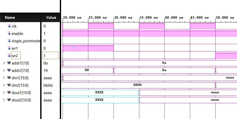
Inthiscase,port1isusedtowritedataintothememoryandport2isusedtoreaddatafromthememory,asillustratedin Fig.2. The signal wr1 = 1 and wr2 = 0. In the first clock cycle, Port 1 writes the data AAAA to address 0A, while Port 2 initially shows undefined output. In the next clock cycle, when Port 2 address is set to 0A, it successfully reads AAAA, confirmingcorrectdual-portoperationandproperdatastorage.
Inthiscase,port2isusedtowritedataintothememoryandport1isusedtoreaddatafromthememory,asillustratedin Fig.3with wr1 = 0 and wr2 = 1.Inthefirstclockcycle,Port2writesthedata BBBB toaddress 14.Inthenextclockcycle, when Port 1 address is set to 14, it successfully reads BBBB, confirming correct data storage and reliable dual-port functionality.
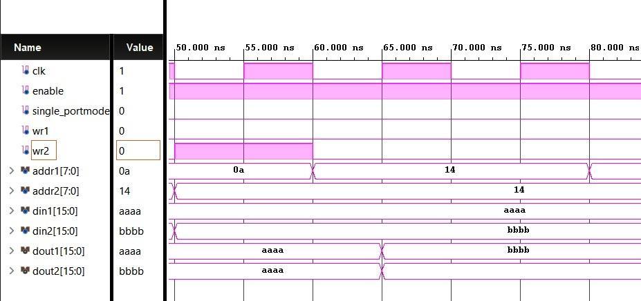
Inthiscase,simultaneousreadoperationfrombothPort1andPort2isdemonstrated asillustratedinFig.4with wr1 = 0 and wr2 = 0.After previouslystoring AAAA ataddress 0A and BBBB ataddress 14,Port1readsfromaddress 0A while Port 2 reads from address 14 in the same clock cycle. The outputs show AAAA and BBBB simultaneously, confirming correctconcurrentreadoperationwithoutinterference.
4: Simultaneous Write
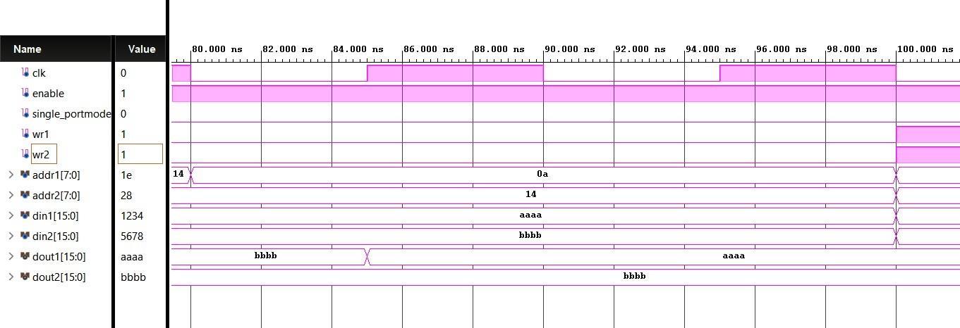
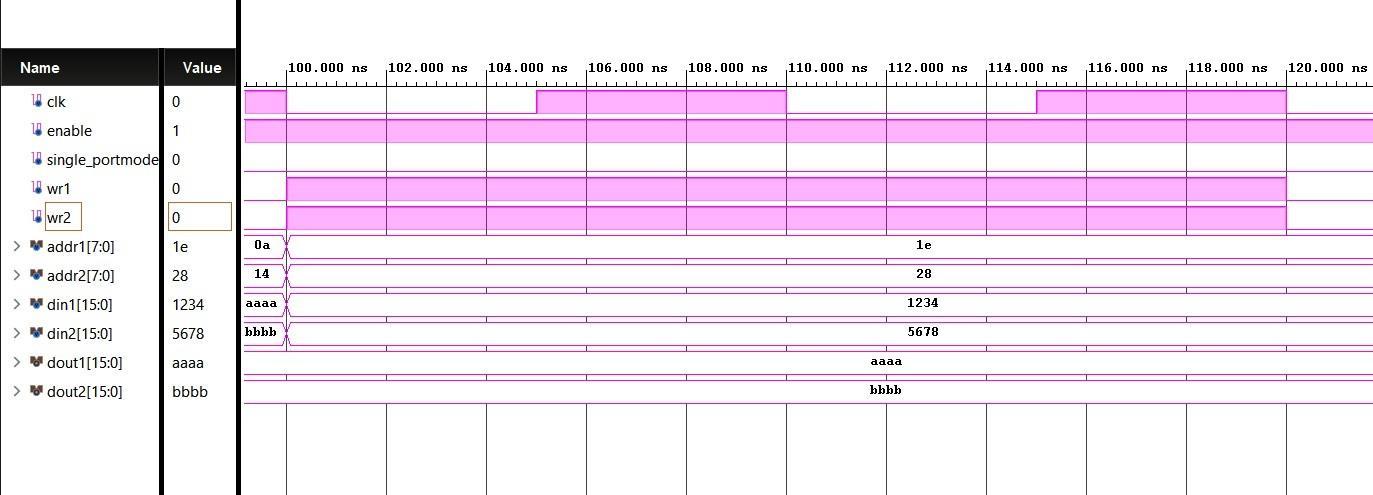
In this case, both ports perform write operations simultaneously with wr1 = 1 and wr2 = 1 to two different address locations as illustrated in Fig.5. In the first clock cycle, Port 1 writes 1234 to address 1E, while Port 2 writes 5678 to address 28.Inthenextclockcycle,withbothportsinreadmode(wr1 = 0, wr2 = 0),Port1reads 1234 andPort2reads 5678,confirmingcorrectsimultaneouswriteoperationwithoutinterference.
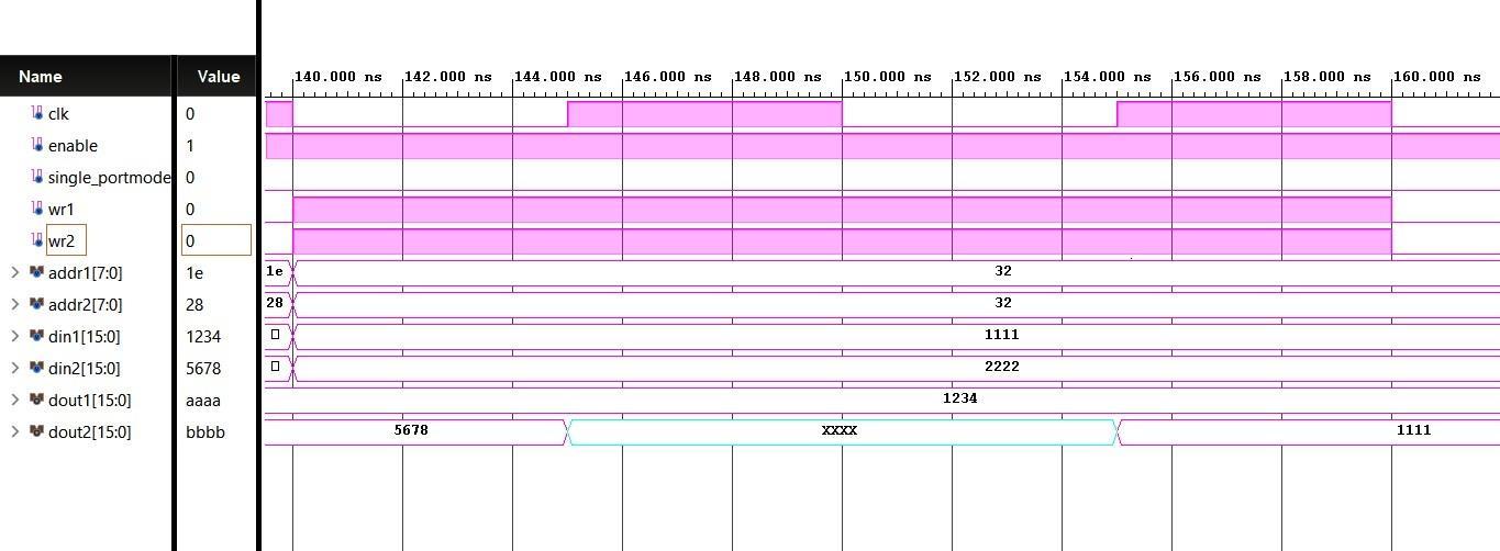
Inthiscase,bothportsattempttowritetothesameaddresswith wr1 = 1 and wr2 = 1 tosameaddresslocationasshown in Fig.6. Port 1 writes 1111 and Port 2 writes 2222 to address 32 in the same clock cycle. In the next clock cycle, when bothportsswitchtoreadmode,theoutputshows 1111,indicatingthatonewriteoperationisprioritizedwhiletheother isignored,therebypreventingdataconflictandensuringmemoryintegrity.
International Research Journal of Engineering and Technology (IRJET) e-ISSN: 2395-0056
Volume: 13 Issue: 03 | Mar 2026 www.irjet.net p-ISSN: 2395-0072
5.SimultaneouswritingfromPort1andPort2todifferentaddresses
International Research Journal of Engineering and Technology (IRJET) e-ISSN: 2395-0056
Volume: 13 Issue: 03 | Mar 2026 www.irjet.net p-ISSN: 2395-0072
4.2 Power Analysis
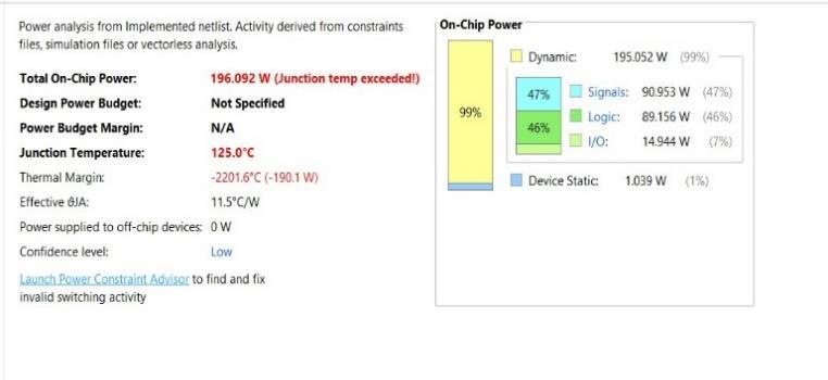
Power analysis of the dual-port RAM was performed by using the Xilinx Vivado power analysis tool. The results show efficient resource utilization and optimized power consumption. The total power that including dynamic and static components, was evaluated to determine the overall energy efficiency of the design and the power consumed by the implementedmemorymoduleisshowninFig.7
4.3 Utilization
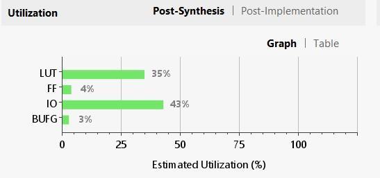
The area utilization of the memory design was analysed by using FPGA resources such as LUTs (Look-Up Tables), FlipFlops(FFs),DSPslices,andBlockRAM(BRAM).TheresultsindicateefficientutilizationofFPGAresourceswhilemeeting therequiredperformanceandfunctionality.TheutilizationreportoftheproposeddesignisshowninFig.8
International Research Journal of Engineering and Technology (IRJET) e-ISSN: 2395-0056
Volume: 13 Issue: 03 | Mar 2026 www.irjet.net p-ISSN: 2395-0072
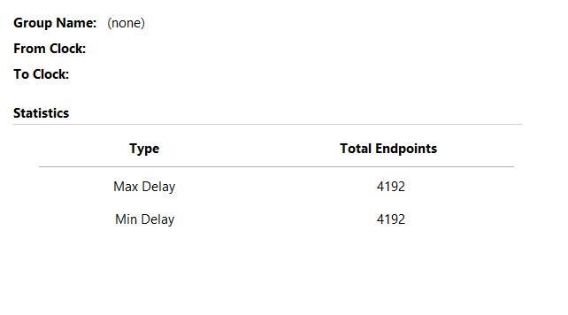
Thedelayanalysisoftheproposeddesign wasperformedusingthe FPGAtiminganalysistool.Thereportindicates4192 endpointsforbothmaximumandminimumdelaypaths,confirmingthatthedesign meetstherequiredtimingconstraints forreliableoperation.Fig.9showsthedelayanalysisofthedesign.
5. Discussion
Our analysis shows how well the suggested synchronous architecture improves timing stability, while the clock gating technique helps in reducing unnecessary switching activity and power consumption. The simulation, timing, and power analysis confirm that the design meets the required performance and resource utilization constraints on the FPGA platformAcomparisonwithexistingmemoryarchitecturesshowsthattheproposeddesignachievesefficientutilizationof FPGA resources while maintaining reliable operation. The comparison with previous works is presented in Table 3 highlightingtheeffectivenessoftheproposeddual-PortRAMarchitectureformoderndigitalsystemapplication
6. CONCLUSION
Our proposed dual-port RAM architecture was successfully designed and implemented using Verilog HDL. The design enables simultaneous access from two independent ports, ensuring proper synchronization and secure data transfer. Functional simulation and FPGA implementation using Xilinx Vivado verified the correctness and stability of the design. Timinganalysisconfirmedthatthememoryoperationssatisfytherequiredtimingconstraints.Thepoweranalysisshowsa total on-chip power consumption of 110 mW, with 15mW dynamic power and 95 mW static power, while the area utilizationis28.3%,demonstratingefficientresourceusage.Overall,theproposeddesignachievesagoodbalancebetween performance, power efficiency, and hardware utilization. The architecture can be further extended to higher data widths such as 32-bit or 64-bit memory and applied in advanced applications like digital signal processing and artificial intelligencesystems.
International Research Journal of Engineering and Technology (IRJET) e-ISSN: 2395-0056
Volume: 13 Issue: 03 | Mar 2026 www.irjet.net p-ISSN: 2395-0072
[1] Abumwais, Allam, and Mahmoud Obaid. "Shared Cache Based on Content Addressable Memory in a Multi-Core Architecture."Computers,Materials&Continua74.3(2023).
[2]N.Rathi,A.Kumar,N.GuptaandS.K.Singh,"AReviewofLowPowerStaticRandomAccessMemory(SRAM)Designs," 2023 IEEE Devices for Integrated Circuit (DevIC), Kalyani, India, 2023, pp. 455 459, doi: 10.1109/DevIC57758.2023.10134887.
[3] Singh, D., Vishnu, C. and Mohan, C.K., 2020, September. Real-time detection of motorcyclist without helmet using cascadeofcnnsonedge-device.In2020IEEE23rdInternationalConferenceonIntelligentTransportationSystems(ITSC) (pp.1-8).IEEE.
[4] W. Che, "FPGA-based memory test system design and test algorithm implementation," 2023 3rd International Conference on Electronic Information Engineering and Computer (EIECT), Shenzhen, China, 2023, pp. 376-380, doi: 10.1109/EIECT60552.2023.10442939.
[5] Y. Ryu et al., "A 16 GB 1024 GB/s HBM3 DRAM With Source Synchronized Bus Design and On-Die Error Control Scheme for Enhanced RAS Features," in IEEE Journal of Solid-State Circuits, vol. 58, no. 4, pp. 10.1109/JSSC.2022.3232096.1051-1061,April2023,doi:
[6]N.Srivastava,A.K.Rajput,M.PattanaikandG.Kaushal,"AnEnergyEfficientandRobust10TSRAMBasedin-Memory Computing Architecture," 2023 36th International Conference on VLSI Design and 2023 22nd International Conference onEmbeddedSystems(VLSID),Hyderabad,India,10.1109/VLSID57277.2023.00039.2023,pp.133-138,doi:
[7]H.Zhan,C.Wang,H.Cui,X.Liu,F.LiuandX.Cheng,"High-SpeedandEnergy-EfficientSingle-PortContentAddressable Memory to Achieve Dual-Port Operation," 2023 Design, Automation & Test in Europe Conference & Exhibition (DATE), Antwerp,Belgium,2023,pp.1-6,doi:10.23919/DATE56975.2023.10137206.
[8] J. Cirimelli-Low et al., "SRAM Design with OpenRAM in SkyWater 130nm," 2023 IEEE International Symposium on CircuitsandSystems(ISCAS),Monterey,CA,USA,2023,pp.1-5,doi:10.1109/ISCAS46773.2023.10181379.
[9]M.C.Chinnaiah,G.D.Vani,D.J.Reddy,K.Bharath,J.S.KiranGoudandN.Kumar,"HEAP-SORTonDualPortRAMBased FPGA," 2023 International Conference on Recent Advances in Electrical, Electronics, Ubiquitous Communication, and ComputationalIntelligence(RAEEUCCI),Chennai,India,2023,pp.1-6,doi:10.1109/RAEEUCCI57140.2023.10134495.
[10] S. Tripathi, S. Choudhary and P. K. Misra, "A Novel STT–SOT MTJ Based Non volatile SRAM for Power Gating Applications," in IEEE Transactions on Electron Devices, vol. 69, no. 3, pp. 1058-1064, March 2022, doi: 10.1109/TED.2022.3140407.
[11] W. Bae, J. -W. Han and K. J. Yoon, "In-Memory Hamming Error Correcting Code in Memristor Crossbar," in IEEE TransactionsonElectronDevices,vol.69,no.7,pp.3700-3707,July2022,doi:10.1109/TED.2022.3176834.
[12]Bhat, Mohammad Waqar,R.Kaartik,and K.B. Sowmya."Designandimplementationofpower efficient clock gated dual-portSRAM."JournalofPhysics:ConferenceSeries.Vol.2325.No.1.IOPPublishing,2022.
[13] C. V. Patil and M. S. Suma, “An alternative test method for the dual port SRAM through the DesignWare SATA AHCI implementation in 3D IC structures,” Engineering Research Express, vol. 4, no. 1, Art. no. 015005, Jan. 2022, doi: 10.1088/2631-8695/ac44fd
[14]T.Nguyen,K.Ngo,N.Trinh,B.Bui,L.Tran,andH.Trang,“EfficientTCAMdesignbasedondualportSRAMonFPGA,” Indonesian Journal of Electrical Engineering and Computer Science, vol. 22, no. 1, pp. 104-112, Apr. 2021, doi: 10.11591/ijeecs.v22.i1.pp104-112
[15] C. Chandrashekar and B. I. Neelgar, “Design and implementation of Dual-Port Memory,” in Journal of University of ShanghaiforScienceandTechnology,vol.23,no.6,pp.1716-1722,June2021.