digi
1 • 2026
64-BIT MPU FOR MASS MARKET IoT
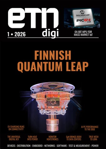
FINNISH QUANTUM LEAP
EV CHARGING RUNS ON CONNECTIVITY THE UNIVERSAL DIGITAL KEY
AI PC PERFORMANCE TO THE EDGE TURN HEAT INTO POWER
MONITOR HEATSTROKES
GaN BRINGS 800V TO DATA CENTERS
TRUE MESH TO LORA
DEVICES - DISTRIBUTION - EMBEDDED - NETWORKS - SOFTWARE - TEST & MEASUREMENT - POWER